User’s Guide SLUUAI4A
Using the UCC28910FBEVM-526 6W Universal Off-Line Flyback
Converter with Primary Side Regulation
1. Introduction:
The UCC28910FBEVM-526 evaluation module is an offline flyback power supply that provides
isolated output voltage and current regulation without the use of an optocoupler. The input
accepts a voltage range of 85VAC to 265VAC.
The evaluation module uses the UCC28910 CV/CC PWM HV Switcher. This device integrates a
700 V power FET and controller that processes operating information from an auxiliary flyback
winding and from the power FET to provide precise output voltage and current control. Control
algorithms in the UCC28910 allow operating efficiencies to meet or exceed applicable standards.
Discontinuous conduction mode (DCM) with valley switching is used to reduce switching losses.
A combination of switching frequency and peak primary current amplitude modulation is used to
keep conversion efficiency high across the full load and input voltage range. Fig.1 below details
the output V-I characteristic
Low system parts count and built in advanced protection features result in a cost-effective
solution that meets stringent world-wide energy efficiency requirements.
This user’s guide provides the schematic, component list, assembly drawing, art work, and test
set up necessary to evaluate the UCC28910 in a typical off-line converter application.
Typical target output V-I Characteristic
Output Voltage (V)
5
±5%
4
±5%
3
2
1
USB Specs. 1.1
Typical Application
0.25
0.5
0.75
1
1.25
1.5
Output Current (A)
Figure1 Output voltage as a function of output load for the UCC28910EVM-526
1 of 22
�User’s Guide SLUUAI4A
2.1 Applications:
The UCC28910 is suited for use in isolated off-line systems requiring high efficiency and
advanced fault protection features including:
USB compliant adapters for cell phones, tablets and cameras
5-7 W AC/DC power supplies
2.2 Features:
The UCC28910FBEVM-526 features include:
Isolated 6W, 5V output
Universal off-line input voltage range
Exceeds Energy Star™ EPS Version 2.0 requirements for active load efficiency and noload power consumption
Meets USB specification 1.1
Meets EN 55022 Class B conducted emissions requirements
Multiple operating modes and valley switching for optimum efficiency over entire
operating range
Primary side control eliminates need for optocoupler
Output over voltage protection
Input under voltage protection
Primary over current protection
Thermal Shutdown
Controlled start up and restart after fault Protection
Caution
High voltage levels are present on the evaluation module whenever it is energized. Proper
precautions must be taken when working with the EVM. The large bulk capacitors, C1 and C2,
and the output capacitors, C7 and C8, must be completely discharged before the EVM can be
handled. Serious injury can occur if proper safety precautions are not followed.
2 of 22
�User’s Guide SLUUAI4A
3. Electrical Performance Specifications
Table1. UCC28910FBEVM-526 Electrical Performance Specifications
Parameter
Symbol
Notes and Conditions
Min Nom
Max Units
INPUT
CHARACTERISTICS
Input Voltage
Frequency
No Load Power
Brownout Voltage
Brownout Recovery
Voltage
Input Current
VIN
fLINE
PNL
VINUVLO
85
47
Vin =Vnom Iout = 0A
IOUT = INOM
VINOV
IIN
Vin =Vmin Iout = max
115/230
50/60
15
70
265
64
20
V
Hz
mW
V
80
V
0.2
A
OUTPUT
CHARACTERISTICS
Output Voltage
Maximum Output
Current
Minimum Output
Current
Output Voltage Ripple
Output Power
VOUT
IOUT(MAX)
Vin =Vmin to VMAX
Iout = 0 to INOM
Vin =Vmin to VMAX
IOUT(MIN) Vin =Vmin to VMAX
ΔVOUT
POUT
Vin =Vmin to VMAX
Iout = 0 to INOM
Vin =Vmin to VMAX
4.75
5
5.25
V
1.14
1.2
1.26
A
0
A
150
mV
75
%
SYSTEM
CHARACTERISTICS
Average Efficiency
η
Vin =Vnom Iout =
25%,50%,75%,100% of
IOUT
ENVIRONMENTAL
Conducted EMI
MECHANICAL
DIMENSIONS
Meets CISPR22B/EN55022B
W
L
H
Width
Length
Component Height
3 of 22
3.5
5
1
in
in
in
�User’s Guide SLUUAI4A
4. Schematic:
Figure2. UCC28910FBEVM-526 schematic
4 of 22
�User’s Guide SLUUAI4A
4.1 Circuit Description:
A brief description of the circuit elements follows:
Diode Bridge D1, input capacitors C1 and C2, transformer T1, UCC28910 switcher U1,
Schottky rectifier D5 and capacitor C7 form the power stage of the converter. Note that
the UCC28910 U1 is also part of the power stage since the high voltage mosfet is internal
to U1
Capacitor C8 filters the high frequency noise directly across the electrolytic output
capacitor.
The input EMI filter is made up of C1 and C2 and differential mode inductors, L2 and L3.
R1,R2 serve the dual function of dampening input filter oscillations and prevent a large
voltage being developed across L2 and L3 in the event of an ESD pulse.
Input current protection is provided by fusible resistor, RF1.
Resistors R5 and R6, capacitor C3, and diodes D2 and D3 make up the primary side
voltage clamp. The clamp prevents the drain voltage on U1 from exceeding its maximum
rating.
A secondary function of the clamp is to alleviate the EMI currents associated with the
turnoff voltage of U1.
Operating bias to the controller is provided by the auxiliary winding on T1, diode D4,
resistor R7 and bulk capacitor C5.
Capacitor C4 is a decoupling capacitor which should always be good quality low
ESR/ESL type capacitors placed as close to the IC pins as possible and returned directly
to the IC ground reference.
Secondary side snubber C6 and R11are used to reduce the effects switching noise of D5.
Resistor R9 programs the start up voltage threshold.
Resistors R8 and R10 program the output voltage set point
Resistors R3 and R4 program the maximum output current
Resistor R12 is used to adjust the no load output voltage
5. EVM Test Set Up:
Figure 3 shows the equipment set up when measuring the input power consumption during no
load. During the no-load test, the power analyzer should be set for long averaging in order to
include several cycles of operation and an appropriate current scale factor should be used. Figure
4 shows the basic test set up recommended to evaluate the UCC28910FBEVM-526 with a load.
Warning
High voltages that may cause injury exist on this evaluation module (EVM). Please ensure all
safety procedures are followed when working on this EVM. Never leave a powered EVM
unattended.
5 of 22
�User’s Guide SLUUAI4A
5.1 Test Equipment:
See Figures 3 and 4 for recommended test set ups.
AC Input Source: The input source shall be an isolated variable AC source
capable of supplying between 85Vrms and 265Vrms at no less than 15W and
connected as shown in Figures 3 and 4. For accurate efficiency calculations, a
power meter should be inserted between the AC source and the EVM. For
highest accuracy, connect the voltage terminals of the power meter directly across
the power source. (Connecting the voltage terminals directly to the EVM will
result in a small current error. This is very significant when measuring no load
power)
Load: For the output load, a programmable electronic load set to constant current
mode and capable of sinking 0 to 1.5ADC at 10VDC shall be used. For highest
accuracy, VOUT can be monitored by connecting a DC voltmeter, DMM V1,
directly across the +Vout and –Vout terminals as shown in Figure3 and Figure4.
A DC current meter, DMM A1, should be placed in series with the electronic load
for accurate output current measurements.
Power Meter: The power analyzer (PM1) shall be capable of measuring low
input current, typically less than 100 uA, and a long averaging mode if low power
standby mode input power measurements are to be taken. An example of such an
analyzer is the Yokogawa WT210 Digital Power Meter. To measure the
intermittent bursts of current and power drawn from the line during no-load
operation, the WT210 should be set to integrate
Multimeters: Two digital multimeters are used to measure the regulated output
voltage (DMM V1) and load current (DMM A1).
Oscilloscope: A digital or analog oscilloscope with a 500MHz scope probe is
recommended
Recommended Wire Gauge: a minimum of AWG 24 wire is recommended.
The wire connections between the AC source and the EVM, and the wire
connections between the EVM and the load should be less than two feet long.
6 of 22
�User’s Guide SLUUAI4A
5.2 Recommended Test Set Up for Operation Without a Load:
V_HI
PM1
V_LO
A_HI
A_LO
LINE
AC
SOURCE
NEUT
+
-
DMM V1
Figure3. UCC28910FBEVM-526 recommended test set up without a load.
5.3 Recommended Test Set Up for Operation With a Load:
V_HI
PM1
V_LO
A_HI
A_LO
+
DMM A1
-
LINE
+
AC
SOURCE
ELECTRONIC
LOAD
NEUT
+
-
-
DMM V1
Figure4. UCC28910FBEVM-526 recommended test set up with a load.
7 of 22
�User’s Guide SLUUAI4A
6. Test Procedure:
All tests should use the set up as described in Section 5 of this user’s guide. The following test
procedure is recommended primarily for power up and shutting down the evaluation module.
Never leave a powered EVM unattended for any length of time.
6.1 Applying Power to the EVM:
1. Set up the EVM as shown in Section 5 of this user’s guide
a. If no-load input power measurements are to be made, set the power analyzer to
long averaging or integrating power measurement mode.
b. For operation with a load, as shown in Figure 4, set the electronic load to constant
current mode to sink 0A.
2. Prior to turning on the AC source, set the voltage to between 85VAC and 265VAC.
3. Turn on the AC source.
4. Monitor the output voltage on DMM V1.
5. Monitor the output current on DMM A1.
6. The EVM is now ready for testing.
6.2 No-Load Power Consumption:
1. Use the test set up shown in Figure 3
a. Set the power analyzer to integrating average power mode.
b. Set the current measurement scale to 0.25A
c. Set the voltage range to 300V
d. Set the measurement mode to RMS
2. Apply power to the EVM per Section 6.1.
3. Monitor the input power on the power analyzer while varying the input voltage.
4. Make sure the input power is off and the bulk capacitor and output capacitors are
completely discharged before handling the EVM.
6.3 Output Voltage Regulation and Efficiency:
1. For load regulation:
a. Use the test set up shown in Figure 4
b. Set the AC source to a constant voltage between 85VAC and 265VAC.
c. Apply power to the EVM per Section 6.1.
d. Vary the load current from 0A up to 1.2A, as measured on DMM A1.
e. Observe that the output voltage on DMM V1 remains between 4.75V and 5.25V
from no load up to 1.2A and thereafter the current remains between 1.14A and
1.26A until the output voltage drops to 2V or lower. See Figure 1 for details.
2. For line regulation:
a. Set the load to sink 1.2A.
b. Vary the AC source from 85VAC to 265VAC.
c. Observe that the output voltage on DMM V1 remains between 4.75V and 5.25V.
8 of 22
�User’s Guide SLUUAI4A
3. Make sure the input power is off and the bulk capacitor and output capacitors are
completely discharged before handling the EVM.
6.4 Output Voltage Ripple:
1. For output ripple measurements, solder a 0.1uF, 50V ceramic and 4.7uF, 35V tantalum
on a BNC adapter as shown in figure 5 below. Connect the red test lead to the +Vout
output and the black test lead to the –Vout on the EVM
2. Connect the other end of the BNC cable to the oscilloscope and monitor the output ripple
on the oscilloscope.
3. Apply power to the EVM per Section 6.1.
Figure5. Typical example of tip measurement technique.
6.5 Equipment Shutdown:
1. Ensure the load is at maximum; this will quickly discharge the output capacitors.
2. Turn off the AC source.
9 of 22
�User’s Guide SLUUAI4A
7. Performance Data and Typical Characteristic Curves:
Figures 6 through 21 present typical performance curves for the UCC28910FBEVM-526.
V-I Characterization
5.500
5.000
4.500
Vout
4.000
120V/60Hz
3.500
3.000
240V/50Hz
2.500
2.000
1.500
0
0.2
0.4
0.6
0.8
1
1.2
Iout
Figure6. Typical V-I Characteristic at 25°C
10 of 22
1.4
�User’s Guide SLUUAI4A
88Vin, Io
0.993
1.013
1.013
1.034
1.056
1.056
1.079
1.079
1.103
1.103
1.128
1.128
1.154
1.154
1.181
1.182
1.211
1.211
1.238
1.238
1.239
1.239
1.240
1.240
1.241
1.242
1.243
1.243
1.243
1.243
1.244
1.244
1.246
1.245
1.247
1.247
1.248
1.248
1.249
1.248
1.250
1.250
1.250
1.251
1.251
1.251
1.252
1.252
88Vin
4.951
4.950
4.950
4.949
4.949
4.949
4.949
4.949
4.949
4.949
4.949
4.949
4.950
4.950
4.950
4.950
4.951
4.951
4.939
4.937
4.820
4.821
4.701
4.700
4.580
4.582
4.463
4.462
4.340
4.338
4.220
4.220
4.100
4.100
3.981
3.981
3.861
3.860
3.737
3.735
3.615
3.615
3.493
3.493
3.370
3.369
3.246
3.248
115in, Io
0.994
1.014
1.014
1.035
1.057
1.057
1.080
1.080
1.104
1.104
1.129
1.129
1.156
1.156
1.183
1.183
1.212
1.212
1.242
1.242
1.245
1.245
1.246
1.246
1.247
1.247
1.248
1.248
1.250
1.249
1.250
1.250
1.251
1.251
1.253
1.252
1.254
1.254
1.255
1.255
1.256
1.255
1.256
1.256
1.257
1.257
1.258
1.258
115Vin
4.953
4.952
4.952
4.952
4.953
4.953
4.953
4.953
4.954
4.954
4.955
4.955
4.956
4.956
4.956
4.956
4.956
4.956
4.957
4.957
4.842
4.841
4.722
4.721
4.602
4.603
4.482
4.481
4.362
4.361
4.240
4.241
4.119
4.118
3.998
3.998
3.877
3.877
3.755
3.756
3.632
3.631
3.510
3.510
3.386
3.385
3.262
3.262
230Vin, Io
0.994
1.014
1.014
1.035
1.057
1.057
1.080
1.080
1.104
1.104
1.130
1.130
1.156
1.156
1.183
1.183
1.212
1.212
1.243
1.243
1.272
1.272
1.274
1.274
1.275
1.275
1.276
1.276
1.277
1.277
1.278
1.278
1.279
1.279
1.280
1.280
1.282
1.282
1.282
1.282
1.284
1.283
1.285
1.284
1.285
1.286
1.287
1.287
11 of 22
230Vin
4.955
4.955
4.955
4.955
4.955
4.955
4.956
4.955
4.956
4.955
4.957
4.956
4.957
4.957
4.958
4.957
4.958
4.958
4.959
4.959
4.947
4.948
4.828
4.826
4.706
4.706
4.583
4.582
4.458
4.460
4.336
4.333
4.211
4.212
4.086
4.085
3.964
3.963
3.837
3.839
3.714
3.714
3.589
3.587
3.462
3.463
3.339
3.337
265Vin, Io
0.994
1.015
1.014
1.035
1.058
1.057
1.080
1.080
1.104
1.104
1.130
1.130
1.156
1.156
1.183
1.183
1.212
1.212
1.243
1.243
1.275
1.275
1.282
1.282
1.284
1.284
1.285
1.285
1.286
1.286
1.288
1.288
1.288
1.288
1.288
1.288
1.291
1.291
1.291
1.292
1.293
1.293
1.294
1.294
1.295
1.295
1.296
1.296
265Vin
4.955
4.955
4.955
4.955
4.955
4.955
4.955
4.955
4.956
4.956
4.956
4.956
4.956
4.957
4.958
4.958
4.958
4.958
4.959
4.959
4.960
4.960
4.860
4.860
4.740
4.738
4.614
4.615
4.491
4.491
4.367
4.368
4.239
4.239
4.112
4.114
3.991
3.990
3.866
3.866
3.740
3.740
3.614
3.615
3.487
3.487
3.362
3.361
�User’s Guide SLUUAI4A
1.253
1.252
1.252
1.253
1.253
1.252
1.253
1.253
1.253
1.252
1.253
1.253
1.253
1.253
1.253
1.253
1.252
1.252
1.251
1.251
1.250
1.250
1.249
1.249
1.248
1.248
1.246
1.246
1.244
1.244
1.241
1.242
0.000
3.124
3.123
2.998
3.000
2.875
2.873
2.752
2.751
2.626
2.623
2.501
2.500
2.376
2.375
2.250
2.249
2.123
2.122
1.997
1.997
1.871
1.870
1.744
1.745
1.618
1.618
1.492
1.492
1.364
1.365
1.238
1.239
0.000
1.258
1.259
1.259
1.259
1.259
1.258
1.260
1.260
1.260
1.260
1.260
1.260
1.260
1.260
1.260
1.259
1.259
1.259
1.258
1.258
1.258
1.258
1.256
1.256
1.254
1.255
1.253
1.253
1.250
1.251
1.248
1.248
0.000
3.139
3.139
3.014
3.013
2.888
2.887
2.763
2.765
2.639
2.639
2.514
2.514
2.388
2.387
2.262
2.262
2.136
2.136
2.009
2.008
1.882
1.882
1.755
1.755
1.627
1.627
1.500
1.500
1.372
1.372
1.246
1.246
0.000
1.288
1.287
1.288
1.288
1.288
1.289
1.289
1.289
1.289
1.289
1.290
1.290
1.290
1.290
1.289
1.290
1.289
1.289
1.289
1.288
1.287
1.288
1.285
1.286
1.285
1.284
1.283
1.283
1.280
1.280
1.278
1.278
0.000
3.209
3.212
3.086
3.083
2.957
2.958
2.830
2.829
2.702
2.701
2.574
2.574
2.445
2.446
2.316
2.316
2.186
2.187
2.057
2.056
1.927
1.926
1.796
1.796
1.666
1.665
1.535
1.537
1.405
1.405
1.275
1.275
0.000
Figure7. Typical V-I Test Data at 25°C
12 of 22
1.296
1.297
1.297
1.298
1.298
1.298
1.299
1.299
1.298
1.299
1.299
1.299
1.300
1.299
1.299
1.299
1.298
1.299
1.298
1.297
1.296
1.296
1.295
1.295
1.294
1.293
1.291
1.291
1.289
1.289
1.287
1.287
0.000
3.234
3.235
3.107
3.106
2.980
2.980
2.850
2.849
2.720
2.721
2.592
2.592
2.464
2.464
2.334
2.334
2.202
2.203
2.072
2.071
1.940
1.940
1.809
1.809
1.678
1.677
1.546
1.548
1.415
1.415
1.284
1.284
0.000
�User’s Guide SLUUAI4A
77
75
73
115V
71
230V
69
67
65
0.1
0.3
0.5
0.7
0.9
1.1
1.3
Figure8. Efficiency Vs Iout
79
77
75
73
71
115V
69
230V
67
65
0.1
1.1
2.1
3.1
4.1
5.1
Figure9. Efficiency Vs Pout
13 of 22
6.1
�User’s Guide SLUUAI4A
Vin(V)
115
230
f(Hz)
60
50
Pin(W)
7.826
5.845
3.889
1.930
7.721
5.783
3.853
1.960
Iout(A)
1.201
0.901
0.601
0.301
1.201
0.901
0.601
0.301
Vout(V) Pout(W)
4.950
5.943
4.942
4.451
4.934
2.964
4.927
1.481
4.956
5.950
4.948
4.457
4.938
2.966
4.930
1.482
Eff (%)
75.94
76.15
76.19
76.73
77.06
77.07
76.97
75.60
Avg Eff (%)
76.25
76.68
Table 1 Average Efficiency
Vin (V)
88
115
230
265
f(Hz)
60
60
50
50
Pin(mW)
10
10
10
12
Vout(V)
5.02
5.02
5.02
5.02
Table 2 No Load Power Consumption
Figure 10 Ripple with 5V,1.2A out 85Vac in
Figure 11 Ripple with 5V,1.2A out 85Vac in
20mV/div 5uS/div
20mV/div 500uS/div
14 of 22
�User’s Guide SLUUAI4A
Figure12 Ripple with 5V,1.2A out 265Vac in
Figure 13 Ripple with 5V,1.2A out 265Vac in
20mV/div 5uS/div
20mV/div 500uS/div
Figure 14 Ripple with 5V,700mA out 265Vac in
Figure 15 Ripple with 5V,100mA out 265Vac in
20mV/div 500uS/div
20mV/div 500uS/div
Figure 16 Output voltage start 115Vac,1.2A load
Figure 17 Output voltage start, 230Vac, 1.2A load
1V/div 50mS/div
1V/div 50mS/div
15 of 22
�User’s Guide SLUUAI4A
Figure 18 Primary side switching waveforms
Figure 19 Primary side switching waveforms
85Vac 1.2A load
265Vac 1.2A load
Drain voltage (CH 3 100V/div) IPK voltage (CH4 0.5V/div)
2uS/div
Drain voltage (CH 3 /div) IPK voltage (CH4 /div)
2uS/div
16 of 22
�User’s Guide SLUUAI4A
Figure20. EMI test results per EN55022, Class B. 115VAC input
17 of 22
�User’s Guide SLUUAI4A
Figure21. EMI test results per EN55022, Class B. 230VAC input
18 of 22
�User’s Guide SLUUAI4A
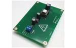
8. EVM Assembly Drawing and Layout:
The following figures show the design of the UCC28910FBEVM-526 printed circuit board.
Figure22. Top side view of UCC28910FBEVM-526
19 of 22
�User’s Guide SLUUAI4A
Figure23. Top layer component placement.
20 of 22
�User’s Guide SLUUAI4A
Figure24. Bottom layer.
21 of 22
�User’s Guide SLUUAI4A
9. List of Materials:
C1
C2
C3
C4
C5
C6
C7
C8
D1
D2
D3
D4
D5
J1, J2
L1, L2
R1, R2, R12
R3,R5
R4
R7
R8
R9
R10
R11
RF1
T1
U1
Description
CAP, AL, 6.8uF, 400V, +/-20%
CAP, AL, 10uF, 400V, +/-20%, 2.864788 ohm
CAP, CERM, 100pF, 500V, +5/%, C0G/NP0, 1206
CAP, CERM, 0.1uF, 25V, +10/%, X5R, 0603
CAP, AL, 10uF, 35V, +/-20%
CAP, CERM, 2200pF, 50V, +/-10%, X7R, 0805
CAP, AL, 1200uF, 10V, +/-20%
CAP, CERM, 0.1uF, 50V, +/-5%, X7R, 1206
Diode, Switching-Bridge, 600V, 1A
Diode, TVS, Uni, 128V, 600W, SMB
Diode, Switching, 600V, 1A
Diode, Ultrafast, 100V, 0.15A, SOD-123
Diode, Schottky, 40V, 4A, SMC
Conn Term Block, 2POS, 5.08mm PCB
Inductor, Drum Core, Metal Composite, 1mH, 0.5A
RES, 6.8k ohm, 5%, 0.25W, 1206
Manufacturer
Nichicon
Panasonic
Kemet
AVX
Nichicon
AVX
Panasonic
AVX
Diodes Inc.
ST Microelectronics
Vishay-Semiconductor
Diodes Inc.
Vishay
Phoenix Contact
Wurth Elektronik eiSos
Vishay-Dale
PartNumber
UCA2G6R8MPD1TD
EEUED2G100
C1206C101JCGACTU
06033D104KAT2A
UVR1V100MDD1TA
08055C222KAT2A
EEUFM1A122
12065C104JAT2A
DF06M
SM6T150A
1N4937-E3
1N4148W-7-F
SL44-E3/57T
1715721
768772102
CRCW12066K80JNEA
Quantity
1
1
1
1
1
1
1
1
1
1
1
1
1
2
2
3
RES, 1.50k ohm, 1%, 0.25W, 1206
RES, 15.0k ohm, 1%, 0.25W, 1206
RES, 33.0 ohm, 1%, 0.25W, 1206
RES, 30.0k ohm, 1%, 0.25W, 1206
RES, 100.0k ohm, 1%, 0.25W, 1206
RES, 430.0k ohm, 1%, 0.25W, 1206
RES, 180 ohm, 5%, 0.25W, 1206
RES, 4.7 ohm, 5%, 1W, Fusible
Transformer, EF16, 1.1mH
LOW STAND-BY POWER, CV / CC PWM HV
SWITCHER WITH PRIMARY SIDE REGULATION
Vishay-Dale
Vishay-Dale
Panasonic
Panasonic
Vishay-Dale
Yageo America
Vishay-Dale
Yageo America
Wurth Elektronik
Texas Instruments
CRCW12061K50FKEA
CRCW120615K0FKEA
ERJ-8ENF33R0V
ERJ-8ENF3002V
CRCW1206100KFKEA
RC1206FR-07430KL
CRCW1206180RJNEA
FKN1WSJR-52-4R7
750313739
UCC28910D
2
1
1
1
1
1
1
1
1
1
Table3. Bill of Materials for UCC28910FBEVM-526
10. References:
1. UCC28910 Datasheet
22 of 22
�IMPORTANT NOTICE
Texas Instruments Incorporated and its subsidiaries (TI) reserve the right to make corrections, enhancements, improvements and other
changes to its semiconductor products and services per JESD46, latest issue, and to discontinue any product or service per JESD48, latest
issue. Buyers should obtain the latest relevant information before placing orders and should verify that such information is current and
complete. All semiconductor products (also referred to herein as “components”) are sold subject to TI’s terms and conditions of sale
supplied at the time of order acknowledgment.
TI warrants performance of its components to the specifications applicable at the time of sale, in accordance with the warranty in TI’s terms
and conditions of sale of semiconductor products. Testing and other quality control techniques are used to the extent TI deems necessary
to support this warranty. Except where mandated by applicable law, testing of all parameters of each component is not necessarily
performed.
TI assumes no liability for applications assistance or the design of Buyers’ products. Buyers are responsible for their products and
applications using TI components. To minimize the risks associated with Buyers’ products and applications, Buyers should provide
adequate design and operating safeguards.
TI does not warrant or represent that any license, either express or implied, is granted under any patent right, copyright, mask work right, or
other intellectual property right relating to any combination, machine, or process in which TI components or services are used. Information
published by TI regarding third-party products or services does not constitute a license to use such products or services or a warranty or
endorsement thereof. Use of such information may require a license from a third party under the patents or other intellectual property of the
third party, or a license from TI under the patents or other intellectual property of TI.
Reproduction of significant portions of TI information in TI data books or data sheets is permissible only if reproduction is without alteration
and is accompanied by all associated warranties, conditions, limitations, and notices. TI is not responsible or liable for such altered
documentation. Information of third parties may be subject to additional restrictions.
Resale of TI components or services with statements different from or beyond the parameters stated by TI for that component or service
voids all express and any implied warranties for the associated TI component or service and is an unfair and deceptive business practice.
TI is not responsible or liable for any such statements.
Buyer acknowledges and agrees that it is solely responsible for compliance with all legal, regulatory and safety-related requirements
concerning its products, and any use of TI components in its applications, notwithstanding any applications-related information or support
that may be provided by TI. Buyer represents and agrees that it has all the necessary expertise to create and implement safeguards which
anticipate dangerous consequences of failures, monitor failures and their consequences, lessen the likelihood of failures that might cause
harm and take appropriate remedial actions. Buyer will fully indemnify TI and its representatives against any damages arising out of the use
of any TI components in safety-critical applications.
In some cases, TI components may be promoted specifically to facilitate safety-related applications. With such components, TI’s goal is to
help enable customers to design and create their own end-product solutions that meet applicable functional safety standards and
requirements. Nonetheless, such components are subject to these terms.
No TI components are authorized for use in FDA Class III (or similar life-critical medical equipment) unless authorized officers of the parties
have executed a special agreement specifically governing such use.
Only those TI components which TI has specifically designated as military grade or “enhanced plastic” are designed and intended for use in
military/aerospace applications or environments. Buyer acknowledges and agrees that any military or aerospace use of TI components
which have not been so designated is solely at the Buyer's risk, and that Buyer is solely responsible for compliance with all legal and
regulatory requirements in connection with such use.
TI has specifically designated certain components as meeting ISO/TS16949 requirements, mainly for automotive use. In any case of use of
non-designated products, TI will not be responsible for any failure to meet ISO/TS16949.
Products
Applications
Audio
www.ti.com/audio
Automotive and Transportation
www.ti.com/automotive
Amplifiers
amplifier.ti.com
Communications and Telecom
www.ti.com/communications
Data Converters
dataconverter.ti.com
Computers and Peripherals
www.ti.com/computers
DLP® Products
www.dlp.com
Consumer Electronics
www.ti.com/consumer-apps
DSP
dsp.ti.com
Energy and Lighting
www.ti.com/energy
Clocks and Timers
www.ti.com/clocks
Industrial
www.ti.com/industrial
Interface
interface.ti.com
Medical
www.ti.com/medical
Logic
logic.ti.com
Security
www.ti.com/security
Power Mgmt
power.ti.com
Space, Avionics and Defense
www.ti.com/space-avionics-defense
Microcontrollers
microcontroller.ti.com
Video and Imaging
www.ti.com/video
RFID
www.ti-rfid.com
OMAP Applications Processors
www.ti.com/omap
TI E2E Community
e2e.ti.com
Wireless Connectivity
www.ti.com/wirelessconnectivity
Mailing Address: Texas Instruments, Post Office Box 655303, Dallas, Texas 75265
Copyright © 2014, Texas Instruments Incorporated
�


 工商网监
湘ICP备2023018690号
工商网监
湘ICP备2023018690号
