application
INFO
available
UCC1581
UCC2581
UCC3581
Micropower Voltage Mode PWM
FEATURES
BLOCK DIAGRAM
• Low 85µA Startup Current
• Low 300µA Operating Current
• Automatically Disabled
Startup Preregulator
• Programmable Minimum Duty
Cycle with Cycle Skipping
• Programmable Maximum
Duty Cycle
• Output Current 1A Peak
Source and Sink
• Programmable Soft Start
• Programmable Oscillator
Frequency
• External Oscillator
Synchronization Capability
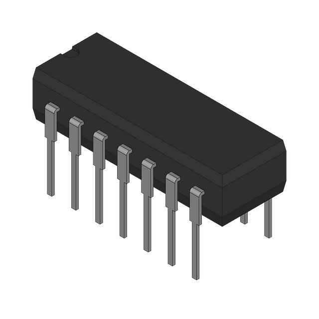
Note: Pin Connection shown for 14-pin Package
UDG-95011-1
DESCRIPTION
The UCC3581 voltage mode pulse width modulator is designed to control low power isolated DC - DC converters
in applications such as Subscriber Line Power (ISDN
I.430). Primarily used for single switch forward and
flyback converters, the UCC3581 features BiCMOS circuitry for low startup and operating current, while maintaining the ability to drive power MOSFETs at
frequencies up to 100kHz. The UCC3581 oscillator allows the flexibility to program both the frequency and the
maximum duty cycle with two resistors and a capacitor. A
TTL level input is also provided to allow synchronization
to an external frequency source.
The UCC3581 includes programmable soft start circuitry,
overcurrent detection, a 7.5V linear preregulator to control chip VDD during startup, and an on-board 4.0V logic
supply.
The UCC3581 provides functions to maximize light load
efficiency that are not normally found in PWM controllers.
MARCH 1999 - REVISED MARCH 2003 - SLUS295B
A linear preregulator driver in conjunction with an external depletion mode N-MOSFET provides initial controller
power. Once the bootstrap supply is functional, the
preregulator is shut down to conserve power. During light
load, power is saved by providing a programmable minimum duty cycle clamp. When a duty cycle below the
minimum is called for, the modulator skips cycles to provide the correct average duty cycle required for output
regulation. This effectively reduces the switching frequency, saving significant gate drive and power stage
losses.
The UCC3581 is available in 14-pin plastic and ceramic
dual-in-line packages and in a 14-pin narrow body small
outline IC package (SOIC). The UCC1581 is specified for
operation from −55°C to +125°C, the UCC2581 is specified for operation from −40°C to +85°C, and the
UCC3581 is specified for operation from 0°C to +70°C.
�UCC1581
UCC2581
UCC3581
CONNECTION DIAGRAMS
ABSOLUTE MAXIMUM RATINGS
Supply Voltage (IDD ≤ 10mA). . . . . . . . . . . . . . . . . . . . . . . . 15V
Supply Current . . . . . . . . . . . . . . . . . . . . . . . . . . . . . . . . . 30mA
VREF Current . . . . . . . . . . . . . . . . . . . . . . . . . . . . . . . . . . –10mA
OUT Current . . . . . . . . . . . . . . . . . . . . . . . . . . . . . . . . . . . . ± 1A
Analog Inputs
EN . . . . . . . . . . . . . . . . . . . . . . . . . . . . –0.3V to (VDD + 0.3V)
VC, ISEN, SYNC, DCMIN. . . . . . . . . . –0.3V to (VREF + 0.3V)
Power Dissipation at TD = 25°C
(N, J, Q, L Package) . . . . . . . . . . . . . . . . . . . . . . . . . . . . . 1W
(D Package) . . . . . . . . . . . . . . . . . . . . . . . . . . . . . . . . . 0.65W
Storage Temperature . . . . . . . . . . . . . . . . . . . –65°C to +150°C
Junction Temperature . . . . . . . . . . . . . . . . . . . –55C to +150°C
Lead Temperature (Soldering, 10 sec.) . . . . . . . . . . . . . +300°C
DIL-14, SOIC-14 (Top View)
N or J, D Packages
Unless otherwise specified, all voltages are with respect to
Ground. Currents positive into, negative out of the specified terminal. Consult Packaging Section of Databook for thermal limitations and considerations of packages.
ORDERING INFORMATION
UCC1581J
UCC2581D
UCC2581N
UCC3581D
UCC3581N
TEMPERATURE RANGE
–55°C to +125°C
–40°C to +85°C
–40°C to +85°C
0°C to +70°C
0°C to +70°C
PACKAGE
CDIP
SOIC
PDIP
SOIC
PDIP
ELECTRICAL CHARACTERISTICS: Unless otherwise stated, these specifications apply for VDD = 10V, 0.1µF capacitor
from VDD to GND, 1.0µF capacitor from REF to GND, RT1 = 680kΩ, RT2 = 12kΩ, CT = 750pF and TA = TJ.
PARAMETER
TEST CONDITIONS
MIN
TYP
MAX UNITS
3.94
4.0
4.06
V
20
45
mV
Reference Section
Output Voltage
I = –0.2mA
Load Regulation
–5.0mA < I < –0.2mA
Undervoltage Lockout Section
Start Threshold
6.7
7.3
7.9
V
Minimum Operating Voltage After Start
6.2
6.8
7.4
V
Hysteresis
0.2
0.5
0.8
V
Linear Preregulator Section
Regulated VDD Voltage
7.0
7.5
8.0
V
Regulated VDD to UVLO Delta
100
230
600
mV
8.2
V
21
kHz
VDD Override Threshold
Oscillator Section
Frequency
25°C
Temperature Stability
(Note 1)
18
3.0
%
CT Peak Voltage
(Note 1)
2.5
V
CT Valley Voltage
(Note 1)
1.0
SYNC VIH
SYNC VIL
19.5
1.9
(Note 1)
2.1
V
2.3
1.8
V
V
PWM SECTION
Maximum Duty Cycle
Minimum Duty Cycle
81
(VC > 1.0V at start of cycle) DCMIN = 1.18V
Input Bias Current
84
(VC < 1.0V) DCMIN = 0V
87
%
0
%
7
10
13
%
(DCMIN), (Note 1)
–150
20
150
nA
(VC), (Note 1)
–150
20
150
nA
2
�UCC1581
UCC2581
UCC3581
ELECTRICAL CHARACTERISTICS: Unless otherwise stated, these specifications apply for VDD = 10V, 0.1µF capacitor
from VDD to GND, 1.0µF capacitor from REF to GND, RT1 = 680kΩ, RT2 = 12kΩ, CT = 750pF and TA = TJ.
PARAMETER
TEST CONDITIONS
MIN
TYP
MAX UNITS
–150
20
150
nA
0.4
0.5
0.6
V
Current Sense Section
Input Bias Current
Overcurrent Threshold
Output Section
OUT Low Level
I = 100mA
0.6
1.2
V
OUT High Level
I = –100mA, VDD – OUT
0.6
1.2
V
Rise/Fall Time
(Note 1)
20
100
ns
–9
–11.5
–14
µA
VIH
1.9
2.0
2.1
V
VIL
1.7
1.8
1.9
V
Hysteresis
180
230
280
mV
5
10
15
µA
85
130
µA
300
600
µA
15
16.5
V
100
150
µA
Soft start Section
Soft start Current
SS = 2V
Chip Enable Section
Source Current
Overall Section
Start-Up Current
VDD < Start Threshold
Operating Supply Current
VC = 0V
VDD Zener Shunt Voltage
IDD = 10mA
IDD Stand-by Shunt Voltage
EN = 0V
13.5
Note 1: Guaranteed by design. Not 100% tested in production
PIN DESCRIPTIONS
CT: Oscillator timing capacitor pin. Minimum value is
100pF.
2 .0V
.
The oscillator charging current is 9. 2 •
RT1
DCMIN: Input for programming minimum duty cycle
where pulse skipping begins. This pin can be grounded
to disable minimum duty cycle feature and pulse
skipping.
See Application Diagram Fig. 1.
2 .0V
.
The current into this pin is
RT1
The value of RT1 should be between 220k and 1MΩ.
EN: Enable input. This pin has an internal 10µA pull-up.
A logic low input inhibits the PWM output and causes the
soft start capacitor to be discharged.
RT2: Resistor pin to program oscillator discharge time.
The minimum value of RT2 is 10kΩ. See Application
Diagram Fig. 1.
GND: Circuit ground.
SS: Soft start capacitor pin. The charging current out of
SS is 3.75X the current in RT1.
GT: Pin for controlling the gate of an external depletion
mode N-MOSFET for the startup supply. The external
N-MOSFET regulates VDD to 7.5V until the bootstrap
supply comes up, then GT goes low.
SYNC: Oscillator synchronization pin. Rising edge
triggered CMOS/TTL compatible input with a 2.1V
threshold. SYNC should be grounded if not used. The
minimum pulse width of the SYNC signal is 100ns.
ISEN: Input for overcurrent comparator. This function can
be used for pulse-by-pulse current limiting. The threshold
is 0.5V nominal.
VC: Control voltage input to PWM comparator. The
nominal control range of VC is 1.0V to 2.5V.
OUT: Gate drive output to external N-MOSFET.
VDD: Chip input power with an 15V internal clamp. VDD
is regulated by startup FET to 7.5V until the bootstrap
voltage comes up. VDD should be bypassed at the chip
with a 0.1µF minimum capacitor.
REF: 4.0V reference output. A minimum value bypass
capacitor of 1.0µF is required for stability.
RT1: Resistor pin to program oscillator charging current.
3
�UCC1581
UCC2581
UCC3581
APPLICATION INFORMATION
The UCC3581’s oscillator allows the user the flexibility to
program the frequency and the duty cycle by adjusting
two resistors and a capacitor. Application Diagram Fig. 1
shows these components as RT1, RT2, and CT. RT1 programs the timing capacitor charging current which results
in a linear ramp charging CT. Discharge of CT is accomplished though RT2 which results in a standard RC discharge waveform. The oscillator on-time (CT charging) is
calculated by the formula
RT2
UCC3581
1
CT
2
GT
3
VDD
RT2
14
SYNC
13
RT1
12
VIN
CT
BSS129 OR
EQUIV.
D2
1µF
t ON = 0.082 • RT1 • CT .
RT1
The off-time (CT discharging) is calculated by the formula
t OFF = 0.95 • RT1 • CT .
Q1
4
OUT
5
GND
6
REF
EN
11
SS
10
CSS
Resistor RT1 programs the charging current. The current
is:
2.0V
.
RT1
REF
CT charging current is 9.2 times the current in RT1. RT1
can range from 220kΩ to 1MΩ. Minimum capacitor size
is 100pF, and minimum RT2 size is 10k.
DCMIN
9
1µF
REF
7
VC
ISEN
8
VIN
U1
D1
A Block Diagram of the Oscillator is shown in Fig. 2. The
oscillator also has an external synchronization pin.
When a low to high level is detected, and if the oscillator’s output is in the high state (CT charging), the oscillator output immediately goes low and CT starts
discharging. The sync input is rising edge sensitive and
is ignored when the oscillator output is low.
REF
REF &
E/A
U1
RL
T1
UDG-99043
Figure 1. Application diagram.
UDG-96105
Figure 2. Oscillator.
4
�UCC1581
UCC2581
UCC3581
APPLICATION INFORMATION (cont.)
The externally bypassed 4.0V reference is controlled by
undervoltage lockout and chip enable circuitry. The enable input is internally tied to a 10µA current source
which allows the pin to be driven by an open collector
driver. The part is also enabled if EN floats. The
UCC3581 has a soft start function which requires a user
supplied external timing capacitor. When in soft start
mode, the soft start capacitor, CSS, is charged with a
constant current source. The soft start current is 3.75X
the current in RT1.
A Typical Micropower Application
The circuit shown in Fig. 3 illustrates the use of the
UCC3581 in a micropower application. The isolated 5V
flyback power supply uses a minimum of parts and operates over an 8:1 input voltage range (15VDC to 120VDC)
while delivering a regulated 5V output with a load swing
from 0W to 1W. It operates in the discontinuous mode at
light load or high line, and continuous mode at heavier
loads and lower line voltages. Higher input line voltages
are possible by simply increasing the voltage ratings of
C1, Q1, D1 and D2.
There is an on-chip control amplifier, which when driving
the gate of an external depletion mode N-MOSFET, acts
as a 7.5V linear preregulator supplying VDD directly from
the primary input power line. The preregulator may subsequently be fully disabled by a tertiary bootstrap winding
providing a minimum of 8.2V to the VDD pin.
The most notable feature of the design is its efficiency.
With a load of 1 watt, the typical efficiency is 82%, dropping to 70% around 50mW. With a load of only 12.5mW,
the efficiency remains as high as 50%. At this load, with
an input of 50V, the total input current is only 500µA.
Note that the power supply can be disabled by pulling the
UCC3581 enable pin low, in which case the input current
drops to less than 150µA.
Computation of DCMIN
DCMIN for a given duty cycle is calculated as follows:
∆V = i OSC • DC •
(t ON + t OFF )
The UCC3581 achieves very low losses by means of low
quiescent current and pulse skipping at light loads which
reduces switching losses. The degree of pulse skipping is
controlled by programming the minimum duty cycle. In
this example, the frequency is 35kHz at maximum load
and drops to