UCC5870-Q1
SLUSD86C – OCTOBER 2019 – REVISED SEPTEMBER 2021
UCC5870-Q1 30-A Isolated IGBT/SiC MOSFET Gate Driver with Advanced Protection
Features for Automotive Applications
– Device HBM ESD classification level 2
– Device CDM ESD classification level C4b
1 Features
•
•
•
•
•
•
•
•
•
•
•
•
•
•
•
•
Split output driver provides 30-A peak source and
30-A peak sink currents
Adjustable "on the fly" gate drive strength
Interlock and shoot-through protection with 150ns(max) propagation delay and programmable
minimum pulse rejection
Primary and Secondary side active short circuit
(ASC) support
Configurable power transistor protections
– DESAT based short circuit protection
– Shunt resistor based overcurrent and short
circuit protection
– NTC based overtemperature protection
– Programmable soft turnoff (STO) and two-level
turnoff (2LTOFF) during power transistor faults
Functional Safety-Compliant
– Developed for functional safety applications
– Documentation available to aid ISO 26262
system design up to ASIL D
Integrated diagnostics:
– Built-in self test (BIST) for protection
comparators
– IN+ to transistor gate path integrity
– Power transistor threshold monitoring
– Internal clock monitoring
– Fault alarm (nFLT1) and warning (nFLT2)
outputs
Integrated 4-A active Miller clamp or optional
external drive for Miller clamp transistor
Advanced high voltage clamping control
Internal and external supply undervoltage and
overvoltage protection
Active output pulldown and default low outputs
with low supply or floating inputs
Driver die temperature sensing and
overtemperature protection
100-kV/µs minimum common mode transient
immunity (CMTI) at VCM = 1000 V
SPI based device reconfiguration, verification,
supervision, and diagnosis
Integrated 10-bit ADC for power transistor
temperature, voltage, and current monitoring
Safety-related certifications:
– 3750 – VRMS isolation for 1 minute per UL1577
(planned)
AEC-Q100 qualified with the following results:
– Device temperature grade 0: –40°C to 125°C
ambient operating temperature
2 Applications
•
•
HEV and EV traction inverter
HEV and EV power modules
3 Description
The UCC5870-Q1 device is an isolated, highly
configurable single-channel gate driver targeted to
drive high power SiC MOSFETs and IGBTs in EV/HEV
applications. Power transistor protections, such
as shunt-resistor–based overcurrent, NTC-based
overtemperature, and DESAT detection, include
selectable soft turn-off or two-level turn-off during
these faults. To further reduce the application size,
the UCC5870-Q1 integrates a 4-A active Miller clamp
during switching, and an active gate pulldown while
the driver is unpowered. An integrated 10-bit ADC
enables monitoring of up to six analog inputs and
the gate driver temperature for enhanced system
management. Diagnostics and detection functions are
integrated to simplify the design of ASIL-D compliant
systems. The parameters and thresholds for these
features are configurable using the SPI interface,
which allows the device to be used with nearly any
SiC MOSFET or IGBT.
Device Information
PART
NUMBER(1)
UCC5870-Q1
(1)
PACKAGE
BODY SIZE (NOM)
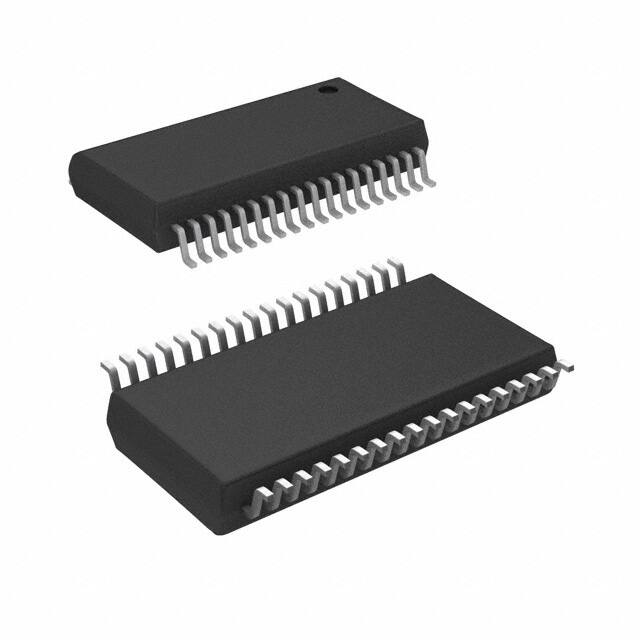
SSOP (36)
12.8 mm × 7.5 mm
For all available packages, see the orderable addendum at
the end of the data sheet.
VI/O
15V to 30V
VCC1
MCU
VCC2
GND2
GND1
DESAT
nFLT1
nFLT2/DOUT
IN+
INnCS
CLK
SDI
SDO
Safety
Controller
ASC
ASC_EN
GND2
VCECLP
SiO2 Isolation Barrier
•
VBST
VEE2
OUTH
OUTL
CLAMP
GND2
GND2
AIx[1:6]
VREG1
VREF
GND1
GND1
GND2 -12V to 0V
VREG2
VEE2
GND2
VEE2
Simplified Schematic
An IMPORTANT NOTICE at the end of this data sheet addresses availability, warranty, changes, use in safety-critical applications,
intellectual property matters and other important disclaimers. PRODUCTION DATA.
�UCC5870-Q1
www.ti.com
SLUSD86C – OCTOBER 2019 – REVISED SEPTEMBER 2021
Table of Contents
1 Features............................................................................1
2 Applications..................................................................... 1
3 Description.......................................................................1
4 Revision History.............................................................. 2
5 Pin Configuration and Functions...................................3
6 Specifications.................................................................. 6
6.1 Absolute Maximum Ratings ....................................... 6
6.2 ESD Ratings .............................................................. 6
6.3 Recommended Operating Conditions ........................6
6.4 Thermal Information ...................................................7
6.5 Power Ratings ............................................................7
6.6 Insulation Specifications ............................................ 7
6.7 Electrical Characteristics ............................................8
6.8 SPI Timing Requirements ........................................ 15
6.9 Switching Characteristics .........................................15
6.10 Typical Characteristics............................................ 17
7 Detailed Description......................................................21
7.1 Overview................................................................... 21
7.2 Functional Block Diagram......................................... 22
7.3 Feature Description...................................................22
7.4 Device Functional Modes..........................................52
7.5 Programming............................................................ 54
7.6 Register Maps...........................................................59
8 Applications and Implementation................................ 98
8.1 Application Information............................................. 98
8.2 Typical Application Using Internal ADC
Reference and Power FET Sense Current
Monitoring..................................................................100
8.3 Typical Application Using DESAT Power FET
Monitoring..................................................................104
9 Power Supply Recommendations..............................107
9.1 VCC1 Power Supply............................................... 107
9.2 VCC2 Power Supply............................................... 107
9.3 VEE2 Power Supply................................................107
9.4 VREF Supply (Optional)..........................................107
10 Layout.........................................................................108
10.1 Layout Guidelines................................................. 108
10.2 Layout Example.................................................... 109
11 Device and Documentation Support........................ 110
11.1 Documentation Support.........................................110
11.2 Receiving Notification of Documentation Updates 110
11.3 Support Resources................................................110
11.4 Trademarks........................................................... 110
11.5 Electrostatic Discharge Caution............................ 110
11.6 Glossary................................................................ 110
12 Mechanical, Packaging, and Orderable
Information.................................................................. 110
4 Revision History
NOTE: Page numbers for previous revisions may differ from page numbers in the current version.
Changes from Revision B (November 2020) to Revision C (July 2021)
Page
• Updated peak currents to the typical value of 30 A and added functional safety information............................ 1
• Updated peak functional safety bullet in features............................................................................................... 1
• Updated features with Q100 bullet..................................................................................................................... 1
• Removed values from VCECLP and DESAT components as these are customer selected.............................. 3
• Updated drive strength to 30 A to align with typical value................................................................................ 24
• Updated secondary side TSD behavior to clarify the functions operation........................................................ 44
• Added information about gate monitoring during secondary side ASC operation............................................ 44
• Corrected equation........................................................................................................................................... 49
• Corrected CONTROL2 bit name in list............................................................................................................. 50
• Corrected CONTROL2 bit name.......................................................................................................................54
• Corrected OVLO1_LEVEL selections...............................................................................................................59
• Updated DESATTH description for clarity.........................................................................................................59
• Updated SPI_FAULT description for clarity.......................................................................................................59
• Corrected OR_NFLT1_SEC and OR_NFLT2_SEC descriptions......................................................................59
• Removed graph to prevent confusion. .............................................................................................................98
Changes from Revision A (June 2020) to Revision B (November 2020)
Page
• Updated marketing status from Advance Information to initial release...............................................................1
2
Submit Document Feedback
Copyright © 2021 Texas Instruments Incorporated
Product Folder Links: UCC5870-Q1
�UCC5870-Q1
www.ti.com
SLUSD86C – OCTOBER 2019 – REVISED SEPTEMBER 2021
5 Pin Configuration and Functions
Figure 5-1. (DWJ) 36-Pin SOIC Top View
Table 5-1. Pin Functions
PIN
I/O(1)
DESCRIPTION
NO.
NAME
1
GND1
G
Primary Side Ground. Connect all GND1 pins together and to the PCB ground plane on the primary side.
2
NC
—
No internal connection. Connect to GND1.
3
NC
—
No internal connection. Connect to GND1.
4
NC
—
No internal connection. Connect to GND1.
5
NC
—
No internal connection. Connect to GND1.
6
ASC_EN
I
Active Short Circuit Enable Input. ASC_EN enables the ASC function and forces the output of the driver to
the state defined by the ASC input. If ASC is high, OUTH is pulled high. If ASC is low, OUTL is pulled low.
See the Active Short Circuit (ASC) section for additional details.
7
nFLT1
O
Fault Indicator Output 1. nFLT1 is used to interrupt the host when a fault occurs. Faults that are unmasked
pull nFLT1 low when the fault occurs. nFLT1 is high when all faults are either non-existent or masked. See
the Fault and Warning Classification section for additional details.
8
nFLT2/DOUT
O
Fault Indicator Output 2. nFLT2 is used to interrupt the host when a fault occurs. Additionally, nFLT2 may
be configured as DOUT to provide the host controller a PWM signal with a duty cycle relative to the ADC
input of interest. Faults that are unmasked pull nFLT2 low when the fault occurs. nFLT2 is high when all
faults are either non-existent or masked. See the Fault and Warning Classification or DOUT Functionality
section for additional details.
9
VCC1
P
Primary Side Power Supply. Connect a 3V to 5.5V power supply to VCC1. Bypass VCC1 to GND1 with
ceramic bulk capacitance as close to the VCC1 pin as possible. See the VCC1, VCC2, VEE2 Bypass
Capacitors section for more details on selecting the values.
10
ASC
I
Active Short Circuit Control Input. ASC sets the drive state when ASC_EN is high. If ASC is high, OUTH
is pulled high. If ASC is low, OUTL is pulled low. See the Active Short Circuit Support (ASC) section for
additional details.
11
IN–
I
Negative PWM Input. IN- is connected to the IN+ from the opposite arm of the half-bridge. If IN+ and INoverlap, the Shoot Through Protection (STP) fault is asserted. See the Shoot-Through Protection section
for additional details.
12
IN+
I
Positive PWM Input. IN+ drives the state of the driver output. With the driver enabled, when IN+ is high,
OUTH is pulled high. When IN+ is low, OUTL is pulled low. Drive IN+ with a 1kHz to 50kHz PWM signal,
with a logic level determined by the VCC1 voltage. IN+ is connected to the IN- of the opposite arm of
the half-bridge. If IN+ and IN- overlap, the Shoot Through Protection (STP) fault is asserted. See the
Shoot-Through Protection section for additional details.
13
CLK
I
SPI Clock. CLK is the clock signal for the main SPI interface. The SPI interface operates with clock rates
up to 4MHz. See the SPI Communication section for more details.
Submit Document Feedback
Copyright © 2021 Texas Instruments Incorporated
Product Folder Links: UCC5870-Q1
3
�UCC5870-Q1
www.ti.com
SLUSD86C – OCTOBER 2019 – REVISED SEPTEMBER 2021
Table 5-1. Pin Functions (continued)
PIN
NO.
I/O(1)
DESCRIPTION
14
nCS
I
SPI Chip Selection Input. nCS is an active low input used to activate the SPI slave device. Drive nCS
low during SPI communication. When nCS is high, the CLK and SDI inputs are ignored. See the SPI
Communication section for more details.
15
SDI
I
SPI Data Input. SDI is the data input for the main SPI interface. Data is sampled on the falling edge of CLK,
SDI must be in a stable condition to ensure proper communication. See the SPI Communication section for
more details.
16
SDO
O
SPI Data Output. SDO is the data output for the main SPI interface. Data is clocked out on the falling edge
of CLK, SDO is changed with a rising edge of CLK. See the SPI Communication section for more details.
17
VREG1
P
Internal Voltage Regulator Output. VREG1 provides a 1.8V rail for internal primary-side circuits. Bypass
VREG1 to GND1 with at least 4.7µF of ceramic capacitance. Do not put any additional load on VREG1.
18
GND1
G
Primary Side Ground. Connect all GND1 pins together and to the PCB ground plane on the primary side.
19
VEE2
P
Secondary Negative Power Supply. Connect all VEE2 supply inputs together. Connect a -12V to 0V power
supply to VEE2. The total voltage rail from VCC2 to VEE2 must not exceed 30V. Bypass VEE2 to GND2
with at least 1uF of ceramic capacitance as close to the VEE1 pin as possible. See the VCC1, VCC2, and
VEE2 Bypass Capacitors section for more details on selecting the values.
20
VREG2
P
Internal voltage regulator output. VREG2 provides a 1.8V rail for internal secondary-side circuits. Bypass
VREG2 to VEE2 with at least 4.7µF of ceramic capacitance. Do not put any additional load on VREG2.
I
Analog Input 6. AI6 is a multi-function input. It is configurable as an input to the internal ADC, a power FET
current sense protection comparator input, and an ASC input for the secondary side. See the Integrated
ADC for Front-End Analog (FEA) Signal Processing section for details on configuring AI6 to be read by
the ADC. See the Shunt Resistor based Overcurrent Protection (OCP) and Short Circuit Protection (SCP)
section for details on configuring AI6 as a power FET current sense protection input. Finally, see the Active
Short Circuit Support (ASC) section for details on configuring AI6 as an ASC input.
I
Analog Input 5. AI5 is a multi-function input. It is configurable as an input to the internal ADC, a power
FET over temperature protection comparator input, and an ASC_EN input for the secondary side. See the
Integrated ADC for Front-End Analog (FEA) Signal Processing section for details on configuring AI5 to be
read by the ADC. See the Temperature Monitoring and Protection for the Power Transistors section for
details on configuring AI5 as a power FET over temperature protection input. Finally, see the Active Short
Circuit Support (ASC) section for details on configuring AI5 as an ASC_EN input.
I
Analog Input 4. AI4 is a multi-function input. It is configurable as an input to the internal ADC and a power
FET current sense protection comparator input. See the Integrated ADC for Front-End Analog (FEA) Signal
Processing section for details on configuring AI4 to be read by the ADC. See the Shunt Resistor based
Overcurrent Protection (OCP) and Short Circuit Protection (SCP) section for details on configuring AI4 as a
power FET current sense protection input.
I
Analog Input 3. AI3 is a multi-function input. It is configurable as an input to the internal ADC and a
power FET current sense protection comparator input. See the Integrated ADC for Front-End Analog (FEA)
Signal Processing section for details on configuring AI3 to be read by the ADC. See the Temperature
Monitoring and Protection for the Power Transistors section for details on configuring AI3 as a power FET
over temperature protection input.
I
Analog Input 2. AI2 is a multi-function input. It is configurable as an input to the internal ADC and a power
FET current sense protection comparator input. See the Integrated ADC for Front-End Analog (FEA) Signal
Processing section for details on configuring AI2 to be read by the ADC. See the Shunt Resistor based
Overcurrent Protection (OCP) and Short Circuit Protection (SCP) section for details on configuring AI2 as a
power FET current sense protection input.
21
22
23
24
25
4
NAME
AI6
AI5
AI4
AI3
AI2
26
AI1
I
Analog Input 1. AI1 is a multi-function input. It is configurable as an input to the internal ADC and a
power FET current sense protection comparator input. See the Integrated ADC for Front-End Analog (FEA)
Signal Processing section for details on configuring AI1 to be read by the ADC. See the Temperature
Monitoring and Protection for the Power Transistors section for details on configuring AI1 as a power FET
over temperature protection input.
27
VREF
P
Internal ADC Voltage Regulator Output. VREF provides an internal 4V, reference for the ADC. Bypass
VREF to GND2 with at least 1uF of ceramic capacitance. If an external reference is desired, disable the
internal VREF using the SPI register, and connect a 4V reference supply to VREF. Loads up to 5mA on
VREF are allowed.
28
GND2
G
Gate Drive Common Input. Connect GND2 to the power FET source/ IGBT emitter. All AIx inputs, VREF,
and DESAT are referenced to GND2.
Submit Document Feedback
Copyright © 2021 Texas Instruments Incorporated
Product Folder Links: UCC5870-Q1
�UCC5870-Q1
www.ti.com
SLUSD86C – OCTOBER 2019 – REVISED SEPTEMBER 2021
Table 5-1. Pin Functions (continued)
PIN
NO.
29
30
NAME
CLAMP
VEE2
I/O(1)
DESCRIPTION
IO
Miller Clamp Input. The CLAMP input is used to hold the gate of the power FET strongly to VEE2 while
the power FET is "off". CLAMP is configurable as an internal Miller clamp, or to drive an external clamping
circuit. When using the internal clamping function, connect CLAMP directly the power FET gate. When
configured as an external clamp, connect CLAMP to the gate of an external pulldown MOSFET. See the
Active Miller Clamp section for additional details.
P
Secondary negative power supply. Connect all VEE2 supply inputs together. Connect a -12V to 0V power
supply to VEE2. The total voltage rail from VCC2 to VEE2 must not exceed 30V. Bypass VEE2 to GND2
with at least 1uF of ceramic capacitance as close to the VEE2 pin as possible. Additional capacitance
may be needed depending on the required drive current. See the VCC1, VCC2, VEE2 Bypass Capacitors
section for more details on selecting the values.
31
OUTL
O
Negative Gate Drive Voltage Output. When the driver is active, OUTL drives the gate of the power FET low
when INP is low. Connect OUTL to the gate of the power FET through a gate resistor. The value of the
gate resistor is chosen based on the slew rate required for the application. See the OUTH/ OUTL Outputs
section for details on choosing the gate resistor.
32
OUTH
O
Positive Gate Drive Voltage Output. When the driver is active, OUTH drives the gate of the power FET high
when INP is high. Connect OUTH to the gate of the power FET through a gate resistor. The value of the
gate resistor is chosen based on the slew rate required for the application. See the OUTH/ OUTL Outputs
section for details on choosing the gate resistor.
33
VBST
P
Bootstrap Supply. VBST supplies power for the OUTH drive. Connect a 0.1µF ceramic capacitor between
VBST and OUTH.
I
VCE Clamp Input. VCECLP clamps to a diode above the VCC2 rail and indicates a fault when the voltage
at VCECLP is above the VCECLPth threshold. Bypass VCECLP to VEE2 with ceramic capacitor and, in
parallel, connect a resistor. Additionally, connect VCECLP to the anode of a zener diode to the collector
of the power FET. For details on selecting the values and ratings for the required components, see the
VCECLP Input section.
P
Secondary Positive Power Supply. Connect a 15V to 30V power supply to VCC2. The total voltage rail
from VCC2 to VEE2 must not exceed 30V. Bypass VCC2 to GND2 and VCC2 to VEE2 with bulk ceramic
capacitance as close to the VCC2 pin as possible. Additional capacitance may be needed depending on
the required drive current. See the VCC1, VCC2, VEE2 Bypass Capacitors section for more details on
selecting the values.
I
Desaturation based Short Circuit Detection Input. DESAT is used to detect a short circuit in the power FET.
Bypass DESAT to GND2 with a ceramic capacitor to program the DESAT blanking time. In parallel, connect
a schottky diode with the cathode connected to the DESAT. Additionally, connect DESAT to a resistor to
the anode of a diode to the collector of the power FET to adjust the DESAT protection threshold. DESAT
detects a fault when the VCE voltage of the power FET exceeds the defined threshold while the power FET
is on. See the DESAT based Short Circuit Protection (DESAT) section for additional details.
34
35
36
(1)
VCECLP
VCC2
DESAT
P = Power, G = Ground, I = Input, O = Output, - = NA
Submit Document Feedback
Copyright © 2021 Texas Instruments Incorporated
Product Folder Links: UCC5870-Q1
5
�UCC5870-Q1
www.ti.com
SLUSD86C – OCTOBER 2019 – REVISED SEPTEMBER 2021
6 Specifications
6.1 Absolute Maximum Ratings
over operating free-air temperature range (unless otherwise noted)(1)
MIN
MAX
UNIT
VCC1
Supply voltage primary side referenced to GND1
–0.3
6
V
VCC2
Positive supply voltage secondary side referenced to GND2
–0.3
33
V
VEE2
Negative supply voltage output side referenced to GND2
–15
0.3
V
VSUP2
Total supply voltage output side (VCC2 - VEE2)
–0.3
33
V
VEE2–0.3
VCC2+0.3
V
–0.3
VCC1+0.3
V
VEE2–0.3
VCC2 +0.3
V
VOUTH, VOUTL Voltage on the driver output pins referenced to GND2
VIOP
Voltage on IO pins (ASC, ASC_EN, CLK, IN+, IN-, nCS,
nFLTx, SDI, SDO) on primary side referenced to GND1
VCLAMP
Voltage on the Miller clamp pin referenced to GND2
VDESAT
Voltage on DESAT referenced to GND2
VCECLP
Voltage on VCECLP referenced to GND2
VREG1
VREG2
–0.3
VCC2 +0.3
V
VEE2–0.3
VCC2 +0.3
V
Voltage on VREG1 referenced to GND1
–0.3
2
V
Voltage on VREG2 referenced to VEE2
–0.3
2
V
VREF
Voltage on VREF referenced to GND2
–0.3
5.5
V
VBST
Voltage on VBST referenced to OUTH
-0.3
5.3
V
VAI
Voltage on the analog inputs referenced to GND2
–0.3
5.5
V
TJ
Junction temperature
–40
150
oC
Tstg
Storage temperature
–65
150
oC
(1)
Operation outside the Absolute Maximum Ratings may cause permanent device damage. Absolute Maximum Ratings do not imply
functional operation of the device at these or any other conditions beyond those listed under Recommended Operating Conditions. If
outside the Recommended Operating Conditions but within the Absolute Maximum Ratings, the device may not be fully functional, and
this may affect device reliability, functionality, performance, and shorten the device lifetime.
6.2 ESD Ratings
VALUE
Human body model (HBM), per AEC
V(ESD)
(1)
Electrostatic discharge
Q100-002(1)
Charged device model (CDM), per AEC
Q100-011
UNIT
±2000
Corner pins (GND1 and VEE2)
±750
Other pins
±500
V
AEC Q100-002 indicates that HBM stressing shall be in accordance with the ANSI/ESDA/JEDEC JS-001 specification.
6.3 Recommended Operating Conditions
over operating free-air temperature range (unless otherwise noted)
MIN
6
NOM
MAX
VCC1
Supply voltage input side
VCC2
Positive supply voltage secondary side (VCC2 - GND2)
VEE2
Negative supply voltage output side (VEE2 - GND2)
VSUP2
Total supply voltage output side (VCC2 - VEE2)
VIH
High-level IO voltage (ASC, ASC_EN, IN+, IN-, nCS, SCLK, SDI)
VIL
Low-level IO voltage (ASC, ASC_EN, IN+, IN-, nCS, SCLK, SDI)
0
0.3*VCC1
IOHP
Source current for primary side outputs (nFLT2, SDO)
IOLP
Sink current for primary side outputs (nFLTx, SDO)
IOH
Driver output source current from OUTH (1)
5.5
V
15
30
V
–12
0
V
15
30
V
0.7*VCC1
VCC1
V
(1)
IOL
Driver output sink current into OUTL
VAI*
Voltage on analog input (AI) pins referenced to GND2
Submit Document Feedback
UNIT
3
0
V
5
mA
5
mA
15
A
15
A
VREF+0.1
V
Copyright © 2021 Texas Instruments Incorporated
Product Folder Links: UCC5870-Q1
�UCC5870-Q1
www.ti.com
SLUSD86C – OCTOBER 2019 – REVISED SEPTEMBER 2021
6.3 Recommended Operating Conditions (continued)
over operating free-air temperature range (unless otherwise noted)
MIN
VVREG1
Output voltage at VREG2 referenced to
VVBST
Ouput voltage at VBST referenced to OUTH(4)
GND2(5)
VVREF
Voltage on the VREF pin vs
CMTI
Common mode transient immunity rating (dV/dt rate across the isolation
barrier)
fPWM
PWM input frequency (IN+ and IN- pins)
fSPI
SPI clock frequency
TJ
Maximum junction temperature
– 40
tPWM
PWM input pulse width (IN+ and IN- pins)
250
MAX
UNIT
1.8
V
1.8
V
Vcc2 + 4.5
V
VEE2(3)
VVREG2
(1)
(2)
(3)
(4)
(5)
NOM
Output voltage at VREG1 referenced to GND1 (2)
0
4
4.1
V
100
kV/us
50
kHz
4
MHz
℃
150
ns
External gate resistor needs to be used to limit the max drive current to be not more than 15A.
Connect a decoupling capacitor of 0.1uF+4.7uF between VREG1 and GND1. Do not connect external supply.
Connect a decoupling capacitor of 0.1uF+4.7uF between VREG2 and VEE2. Do not connect external supply.
Connect a decoupling capacitor of 100nF between VBST and OUTH. Do not connect external supply.
Connect a decoupling capacitor of 1.0uF on the VREF pin.
6.4 Thermal Information
UCC5870
THERMAL METRIC(1)
DWJ
UNIT
36 SOIC
RθJA
Junction-to-ambient thermal resistance
50.6
°C/W
RθJC(top)
Junction-to-case (top) thermal resistance
17.5
°C/W
RθJB
Junction-to-board thermal resistance
21.3
°C/W
ΨJT
Junction-to-top characterization parameter
5.3
°C/W
ΨJB
Junction-to-board characterization parameter
20.2
°C/W
RθJC(bot)
Junction-to-case (bottom) thermal resistance
N/A
°C/W
(1)
For more information about traditional and new thermal metrics, see the Semiconductor and IC Package Thermal Metrics application
report.
6.5 Power Ratings
PARAMETER
TEST CONDITIONS
MIN
TYP
MAX
UNIT
PD
Maximum power dissipation (both sides)
TA = 125C
500
mW
PD1
Maximum power dissipation (side-1)
TA = 125C
50
mW
PD2
Maximum power dissipation (side-2)
TA = 125C
450
mW
6.6 Insulation Specifications
PARAMETER
SPECIFIC
ATION
TEST CONDITIONS
UNIT
PACKAGE SPECIFICATIONS
CLR
External clearance(1)
Shortest terminal-to-terminal distance through air 8
mm
CPG
External creepage(1)
Shortest terminal-to-terminal distance across the
package surface
8
mm
DTI
Distance through the insulation
Minimum internal gap (internal clearance)
> 17
µm
CTI
Comparative tracking index
DIN EN 60112 (VDE 0303-11); IEC 60112
600
V
Material group
According to IEC60664-1
I
Submit Document Feedback
Copyright © 2021 Texas Instruments Incorporated
Product Folder Links: UCC5870-Q1
7
�UCC5870-Q1
www.ti.com
SLUSD86C – OCTOBER 2019 – REVISED SEPTEMBER 2021
6.6 Insulation Specifications (continued)
PARAMETER
SPECIFIC
ATION
TEST CONDITIONS
Rated mains voltage ≤ 600 VRMS
I-IV
Rated mains voltage ≤ 1000 VRMS
I-III
VIO = 0.4 × sin (2 πft), f = 1 MHz
2
VIO = 500 V, TA = 25°C
10^12
Insulation resistance, input to output(2)
VIO = 500 V, 100°C ≤ TA ≤ 125°C
10^11
VIO = 500 V at TS = 150°C
10^9
Withstand isolation voltage
VTEST = VISO = 3750 VRMS, t = 60 s (qualification),
VTEST = 1.2 × VISO = 4500 VRMS, t = 1 s (100%
3750
production)
Overvoltage category
UNIT
UL 1577
Barrier capacitance, input to output(2)
CIO
RIO
VISO
(1)
(2)
pF
Ω
VRMS
Creepage and clearance requirements should be applied according to the specific equipment isolation standards of an application.
Care should be taken to maintain the creepage and clearance distance of a board design to ensure that the mounting pads of the
isolator onthe printed-circuit board do not reduce this distance. Creepage and clearance on a printed-circuit board become equal
in certain cases.Techniques such as inserting grooves, ribs, or both on a printed-circuit board are used to help increase these
specifications.
All pins on each side of the barrier tied together creating a two-pin device.
6.7 Electrical Characteristics
Over recommended operating conditions unless otherwise noted.
PARAMETER
TEST CONDITIONS
MIN
TYP
MAX
UNIT
POWER SUPPLY
VIT+
(UVLO1)
VIT+
(UVLO1)
VIT(UVLO1)
VIT(UVLO1)
VHYS
(UVLO1)
tUVLO1
VIT(OVLO1)
VIT(OVLO1)
VIT+
(OVLO1)
VIT+
(OVLO1)
VHYS
(OVLO1)
tOVLO1
VIT+
(UVLO2)
8
UVLO threshold of VCC1 rising
UVOV1_LEVEL = 0
2.6
2.75
2.9
V
UVLO threshold of VCC1 rising
UVOV1_LEVEL = 1
4.5
4.65
4.8
V
UVLO threshold of VCC1 falling
UVOV1_LEVEL = 0
2.3
2.45
2.6
V
UVLO threshold of VCC1 falling
UVOV1_LEVEL = 1
4.2
4.35
4.5
V
UVLO threshold hysteresis of VCC1
VCC1 UVLO detection deglitch time
0.30
V
20
µs
OVLO threshold of VCC1 falling
UVOV1_LEVEL = 0
3.7
3.85
4.0
V
OVLO threshold of VCC1 falling
UVOV1_LEVEL = 1
5.2
5.35
5.5
V
OVLO threshold of VCC1 rising
UVOV1_LEVEL = 0
4.0
4.15
4.3
V
OVLO threshold of VCC1 rising
UVOV1_LEVEL = 1
5.5
5.65
5.8
V
OVLO threshold hysteresis of VCC1
0.30
VCC1 OVLO detection deglitch time
UVLO threshold voltage of
VCC2 rising with reference to GND2
V
20
µs
UVLO2TH = 00b
15.2
16
16.8
V
UVLO2TH = 01b
13.3
14
14.7
V
UVLO2TH = 10b
11.4
12
12.6
V
UVLO2TH = 11b
9.5
10
10.5
V
Submit Document Feedback
Copyright © 2021 Texas Instruments Incorporated
Product Folder Links: UCC5870-Q1
�UCC5870-Q1
www.ti.com
SLUSD86C – OCTOBER 2019 – REVISED SEPTEMBER 2021
6.7 Electrical Characteristics (continued)
Over recommended operating conditions unless otherwise noted.
PARAMETER
VIT(UVLO2)
VHYS
UVLO threshold voltage of
VCC2 falling with reference to GND2
(UVLO2)
UVLO threshold voltage hysteresis of
VCC2
tUVLO2
VCC2 UVLO detection deglitch time
VIT(OVLO2)
VIT+
(OVLO2)
VHYS
OVLO threshold voltage of
VCC2 falling with reference to GND2
OVLO threshold voltage of
VCC2 rising with reference to GND2
MIN
TYP
MAX
UNIT
UVLO2TH = 00b
TEST CONDITIONS
14.25
15
15.75
V
UVLO2TH = 01b
12.35
13
13.65
V
UVLO2TH = 10b
10.45
11
11.55
V
UVLO2TH = 11b
8.55
9
9.45
V
1
V
20
µs
OVLO2TH = 00b
21.85
23
24.15
V
OVLO2TH = 01b
19.95
21
22.05
V
OVLO2TH = 10b
18.05
19
19.95
V
OVLO2TH = 11b
16.15
17
17.85
V
OVLO2TH = 00b
22.8
24
25.2
V
OVLO2TH = 01b
20.9
22
23.1
V
OVLO2TH = 10b
19
20
21
V
OVLO2TH = 11b
17.1
18
18.9
V
(OVLO2)
OVLO threshold voltage hysteresis of
VCC2
1
V
tOVLO2
VCC2 OVLO detection blanking time
20
µs
VIT(UVLO3)
VIT+
(UVLO3)
VHYS
UVLO threshold voltage of VEE2
falling with reference to GND2
UVLO threshold voltage of VEE2
rising with reference to GND2
(UVLO3)
UVLO threshold voltage hysteresis of
VEE2
tUVLO3
VEE2 UVLO detection blanking time
VIT+
(OVLO3)
VIT(OVLO3)
VHYS(OVL
OVLO threshold voltage of VEE2 rising
with reference to GND2
OVLO threshold voltage of VEE2
falling with reference to GND2
UVLO3TH = 00b
–3.15
–3
–2.85
V
UVLO3TH = 01b
–5.25
–5
–4.75
V
UVLO3TH = 10b
–8.4
–8
–7.6
V
UVLO3TH = 11b
–10.5
–10
–9.5
V
UVLO3TH = 00b
–2.1
–2
–1.9
V
UVLO3TH = 01b
–4.2
–4
–3.8
V
UVLO3TH = 10b
–7.35
–7
–6.65
V
UVLO3TH = 11b
–9.45
–9
–8.55
V
1
V
20
OVLO3TH = 00b
–5.25
OVLO3TH = 01b
OVLO3TH = 10b
µs
–5
–4.75
V
–7.35
–7
–6.65
V
–10.5
–10
–9.5
V
OVLO3TH = 11b
–12.6
–12
–11.4
V
OVLO3TH = 00b
–6.3
–6
–5.7
V
OVLO3TH = 01b
–8.4
–8
–7.6
V
OVLO3TH = 10b
–11.55
–11
–10.45
V
OVLO3TH = 11b
–13.65
–13
–12.35
V
O3)
OVLO threshold voltage hysteresis of
VEE2
1
V
tOVLO3
VEE2 OVLO detection blanking time
20
µs
IQVCC1
Quiescent Current of VCC1
No switching, VCC1 = 5V
7.7
mA
IQVCC2
Quiescent Current of VCC2
No switching, VCC2 = 20V, VEE2 = -10V
15
mA
IQVEE2
Quiescent Current of VEE2
No switching, VCC2 = 20V, VEE2 = -10V
15
mA
tRP(VCC1)
Slew rate of VCC1
0.1
V/µs
tRP(VCC2)
Slew rate of VCC2
0.1
V/µs
Submit Document Feedback
Copyright © 2021 Texas Instruments Incorporated
Product Folder Links: UCC5870-Q1
9
�UCC5870-Q1
www.ti.com
SLUSD86C – OCTOBER 2019 – REVISED SEPTEMBER 2021
6.7 Electrical Characteristics (continued)
Over recommended operating conditions unless otherwise noted.
PARAMETER
tRP(VEE2)
TEST CONDITIONS
MIN
TYP
Slew rate of VEE2
MAX
UNIT
0.1
V/µs
LOGIC IO
VIH
VIL
VHYS(IN)
ILI
RPUI
RPDI
Input-high threshold voltage of primary
IO (IN+, IN-, ASC, and ASC_EN)
Input rising, VCC1 = 3.3V
Input-high threshold voltage of
secondary IO in ASC mode (AI5, and
AI6)
Input rising, VREF=4V
Input-low threshold voltage of primary
IO (IN+, IN-, ASC, and ASC_EN)
VCC1 = 3.3V
Input-low input-threshold voltage of
secondary IO in ASC mode (AI5 and
AI6)
Input falling
Input hysteresis voltage of primary IO
(IN+, IN-, ASC, and ASC_EN)
VCC1=3.3V
V
1.5
V
0.1*VCC1
V
0.5
V
5
µA
Leakage current on nCS
VIO = VCC1, VIO is the voltage on IO pins
5
µA
Pullup resistance for nCS
40
100
kΩ
Pulldown resistance for ASC, ASC_EN,
IN+, IN-, CLK, and SDI
40
100
kΩ
800
1200
kΩ
4.5mA output current, VCC1 = 5V
VOL
Output logic-low voltage (nFLT1, nFLT2,
and SDO)
4.5mA sink current, VCC1 = 5V
Output frequency of DOUT pin
RPUO
V
VIO = GND1, VIO is the voltage on IO pins
Output logic-high voltage (SDO)
ILO
3.0
Leakage current on the input IO pins
ASC, ASC_EN, IN+, IN-, CLK, and SDI
VOH
DDOUT
V
0.3*VCC1
Input hysteresis voltage of secondary IO
in ASC mode (AI5, and AI6)
Pulldown resistance for AI5 and AI6 in
ASC mode
fDOUT
0.7*VCC1
Duty of DOUT
0.9*VCC1
V
0.1*VCC1
V
FREQ_DOUT = 00b
13.9
kHz
FREQ_DOUT = 01b
27.8
kHz
FREQ_DOUT = 10b
55.7
kHz
FREQ_DOUT = 11b
111.4
kHz
VAI* = 0.36 V
10
%
VAI* = 1.8 V
50
%
VAI* = 3.24 V
90
%
Leakage current on pin nFLT*
nFLT* = HiZ, VCC1 on nFLT* pin
–5
5
µA
Leakage current on pin SDO
nCS = 1
–5
5
µA
40
100
kΩ
Pullup resistance for pin nFLT*
DRIVER STAGE
VOUTH
High-level output voltage (OUT and
OUTH)
IOUT = -100 mA
VOUTL
Low-level output voltage (OUT and
OUTL)
IOUT = 100 mA
IOUTH
Gate driver high output current
IN+= high, IN- = low, VCC2 - VOUTH = 5
V
15
A
IOUTL
Gate driver low output current
IN- = low, IN + = high, VOUTL - VEE2 = 5
V
15
A
10
Submit Document Feedback
VCC2 –
0.033
V
33
mV
Copyright © 2021 Texas Instruments Incorporated
Product Folder Links: UCC5870-Q1
�UCC5870-Q1
www.ti.com
SLUSD86C – OCTOBER 2019 – REVISED SEPTEMBER 2021
6.7 Electrical Characteristics (continued)
Over recommended operating conditions unless otherwise noted.
PARAMETER
ISTO
Driver low output current during SC and
OC faults
MIN
TYP
MAX
UNIT
VOUTL - VEE2 = 6 V and STO_CURR =
00b, 100℃ to 150℃
TEST CONDITIONS
0.24
0.3
0.36
A
VOUTL - VEE2 = 6 V and STO_CURR =
01b, 100℃ to 150℃
0.48
0.6
0.72
A
VOUTL - VEE2 = 6 V and STO_CURR =
10b, 100℃ to 150℃
0.72
0.9
1.08
A
VOUTL - VEE2 = 6 V and STO_CURR =
11b, 100℃ to 150℃
0.96
1.2
1.44
A
100
mV
ACTIVE MILLER CLAMP
VCLP
VCLPTH
Low-level clamp voltage (internal Miller
clamp)
ICLP = 100 mA
Miller clamp current
MCLPTH=11b, VCLAMP = VEE2+4 V
3.2
MCLPTH = 00b
1.2
1.5
1.8
V
MCLPTH = 01b
1.6
2
2.5
V
MCLPTH = 10b
2.25
3
3.75
V
MCLPTH = 11b
3
4
5
V
4.5
5
5.5
V
Clamp threshold voltage with reference
to VEE2
A
VECLP
CLAMP output voltage in external Miller
clamp mode
RECLP_PD
CLAMP pulldown resistance in external
Miller clamp mode
13
Ω
RECLP_PU
CLAMP pull-up resistance in external
Miller clamp mode
13
Ω
SHORT CIRCUIT CLAMPING
VCLP-OUT
Clamping voltage (VOUTH - VCC2, VCLAMP IN+= high, IN- = low, tCLP = 10us, IOUTH or
- VCC2)
ICLAMP = 500 mA
0.8
1.6
V
1.55
V
2.5
V
ACTIVE PULLDOWN
VOUTSD
Active shut-down voltage on OUTL
IOUTL = 30mA, VCC2 = open
VOUTSD
Active shut-down voltage on OUTL
IOUTL = 0.1xIOUTL, VCC2 = open
DESAT SHORT-CIRCUIT PROTECTION
VDESATth
VDESATL
DESAT detection threshold voltage wrt
GND2
DESATTH = 0000b
2.25
2.5
2.75
V
DESATTH = 0001b
2.7
3
3.3
V
DESATTH = 0010b
3.15
3.5
3.85
V
DESATTH = 0011b
3.6
4
4.4
V
DESATTH = 0100b
4.05
4.5
4.95
V
DESATTH = 0101b
4.5
5
5.5
V
DESATTH = 0110b
4.95
5.5
6.05
V
DESATTH = 0111b
5.4
6
6.6
V
DESATTH = 1000b
5.85
6.5
7.15
V
DESATTH = 1001b
6.3
7
7.7
V
DESATTH = 1010b
6.75
7.5
8.25
V
DESATTH = 1011b
7.2
8
8.8
V
DESATTH = 1100b
7.65
8.5
9.35
V
DESATTH = 1101b
8.1
9
9.9
V
DESATTH = 1110b
8.55
9.5
10.45
V
DESATTH = 1111b
9
10
11
V
1
V
DESAT voltage with respect to GND2
when OUTL is driven low
Submit Document Feedback
Copyright © 2021 Texas Instruments Incorporated
Product Folder Links: UCC5870-Q1
11
�UCC5870-Q1
www.ti.com
SLUSD86C – OCTOBER 2019 – REVISED SEPTEMBER 2021
6.7 Electrical Characteristics (continued)
Over recommended operating conditions unless otherwise noted.
PARAMETER
ICHG
Blanking capacitor charging current
MIN
TYP
MAX
UNIT
V(DESAT) - GND2 = 2 V,
DESAT_CHG_CURR = 00b
TEST CONDITIONS
0.555
0.6
0.645
mA
V(DESAT) - GND2 = 2 V,
DESAT_CHG_CURR = 01b
0.6475
0.7
0.7525
mA
V(DESAT) - GND2 = 2 V,
DESAT_CHG_CURR = 10b
0.74
0.8
0.86
mA
V(DESAT) - GND2 = 2 V,
DESAT_CHG_CURR = 11b
0.925
1
1.075
mA
127
158
250
ns
IDCHG
Blanking capacitor discharging current
tLEB
DESAT leading edge blanking time
V(DESAT) - GND2 = 6 V
14
mA
tDESFLT
DESAT pin glitch filter
DESAT_DEGLITCH=0
90
158
190
ns
tDESFLT
DESAT pin glitch filter
DESAT_DEGLITCH=1
270
316
401
ns
tDESAT
(90%)
DESAT protection reaction time from
event to action (includes deglitch time)
VDESAT>VDESATth to VOUTL 90% of VCC2,
CLOAD = 1 nF, DESAT_DEGLITCH=0
160 +
tDESFLT
ns
OVERCURRENT PROTECTION
VOCth
Over current detection threshold voltage
VSCth
Short circuit protection threshold
tSCBLK
12
OCTH = 0000b
170
200
225
mV
OCTH = 0001b
220
250
275
mV
OCTH = 0010b
270
300
330
mV
OCTH = 0011b
315
350
375
mV
OCTH = 0100b
360
400
440
mV
OCTH = 0101b
410
450
475
mV
OCTH = 0110b
460
500
525
mV
OCTH = 0111b
520
550
575
mV
OCTH = 1000b
570
600
630
mV
OCTH = 1001b
610
650
690
mV
OCTH = 1010b
660
700
740
mV
OCTH = 1011b
710
750
790
mV
OCTH = 1100b
760
800
840
mV
OCTH = 1101b
807
850
893
mV
OCTH = 1110b
855
900
945
mV
OCTH = 1111b
902
950
998
mV
SCTH = 00b
460
500
530
mV
SCTH = 01b
700
750
785
mV
SCTH = 10b
945
1000
1050
mV
SCTH = 11b
1185
1250
1312
mV
SC_BLK = 00b
100
ns
Short circuit protection blanking time with SC_BLK = 01b
reference to system clock
SC_BLK = 10b
200
ns
400
ns
SC_BLK = 11b
800
ns
Submit Document Feedback
Copyright © 2021 Texas Instruments Incorporated
Product Folder Links: UCC5870-Q1
�UCC5870-Q1
www.ti.com
SLUSD86C – OCTOBER 2019 – REVISED SEPTEMBER 2021
6.7 Electrical Characteristics (continued)
Over recommended operating conditions unless otherwise noted.
PARAMETER
tOCBLK
Over current protection blanking time
with reference to system clock
TEST CONDITIONS
MIN
TYP
MAX
UNIT
OC_BLK = 000b
500
ns
OC_BLK = 001b
1000
ns
OC_BLK = 010b
1500
ns
OC_BLK = 011b
2000
ns
OC_BLK = 100b
2500
ns
OC_BLK = 101b
3000
ns
OC_BLK = 110b
5000
ns
OC_BLK = 111b
10000
ns
tSCFLT
Short circuit protection deglitch filter
50
150
200
ns
tOCFLT
Over current protection deglitch filter
50
150
200
ns
tSC(90%)
Short circuit protection reaction time from VAIx > VSCth to VOUTL at 90% of VCC2,
event to action (includes deglitch time)
CLOAD = 1nF, tSCBLK expired
tOC(90%)
Over current protection reaction time
from event to action (includes deglitch
time)
175
+ tSCFLT
VAIx > VOCth to VOUTL at 90% of VCC2,
CLOAD = 1nF, tOCBLK expired
ns
175 +
tOCFLT
ns
TWO-LEVEL TURN-OFF PLATEAU VOLTAGE LEVEL
V2 LOFF
t2 LOFF
I2 LOFF
2LOFF_VOLT = 000b
5
6
7
V
2LOFF_VOLT = 001b
6
7
8
V
2LOFF_VOLT = 010b
7
8
9
V
Plateau voltage (w.r.t. GND2) during two- 2LOFF_VOLT = 011b
level turnoff
2LOFF_VOLT = 100b
8
9
10
V
9
10
11
V
2LOFF_VOLT = 101b
10
11
12
V
2LOFF_VOLT = 110b
11
12
13
V
2LOFF_VOLT = 111b
12
13
14
V
Plateau voltage during two-level turnoff
hold time
Discharge current for transition to
plateau voltage level
2LOFF_TIME = 000b
150
ns
2LOFF_TIME = 001b
300
ns
2LOFF_TIME = 010b
450
ns
2LOFF_TIME = 011b
600
ns
2LOFF_TIME = 100b
1000
ns
2LOFF_TIME = 101b
1500
ns
2LOFF_TIME = 110b
2000
ns
2LOFF_TIME = 111b
2500
ns
2LOFF_CURR = 00b, 100℃ to 150℃
0.24
0.3
0.36
A
2LOFF_CURR = 01b, 100℃ to 150℃
0.48
0.6
0.72
A
2LOFF_CURR = 10b, 100℃ to 150℃
0.72
0.9
1.08
A
2LOFF_CURR = 11b, 100℃ to 150℃
0.96
1.2
1.44
A
1.5
2.2
2.9
V
HIGH VOLTAGE CLAMPING
VCECLPTH
VCE clamping threshold with respect to
VEE2
VCECLPHY
VCE clamping threshold hysteresis
S
tVCECLP
tVCECLP_H
LD
VCE clamping intervention-time
VCE clamping hold on time
200
mV
30
ns
VCE_CLMP_HLD_TIME = 00b
100
ns
VCE_CLMP_HLD_TIME = 01b
200
ns
VCE_CLMP_HLD_TIME = 10b
300
ns
VCE_CLMP_HLD_TIME = 11b
400
ns
Submit Document Feedback
Copyright © 2021 Texas Instruments Incorporated
Product Folder Links: UCC5870-Q1
13
�UCC5870-Q1
www.ti.com
SLUSD86C – OCTOBER 2019 – REVISED SEPTEMBER 2021
6.7 Electrical Characteristics (continued)
Over recommended operating conditions unless otherwise noted.
PARAMETER
TEST CONDITIONS
MIN
TYP
MAX
UNIT
OVERTEMPERATURE PROTECTION
TSD_SET
Overtemperature protection set for driver
155
°C
TSD_CLR
Overtemperature protection clear for
driver
135
°C
TWN_SET
Overtemperature warning set for driver
130
°C
TWN_CLR
Overtemperature warning clear for driver
110
THYS
Hysteresis for thermal comparators
Bias current for temp sensing diode for
pins AI1, AI3, and AI5
ITO
VPS_TSDth
°C
20
The threshold of power switch over
temperature protection.
tPS_TSDFL Power switch thermal shutdown deglitch
time
T
°C
TEMP_CURR = 00b, Tj = 100C to 150C
0.097
0.1
0.103
mA
TEMP_CURR = 01b, Tj = 100C to 150C
0.291
0.3
0.309
mA
TEMP_CURR = 10b, Tj = 100C to 150C
0.582
0.6
0.618
mA
TEMP_CURR = 11b, Tj = 100C to 150C
0.97
1
1.03
mA
TSDTH_PS = 000b
0.95
1
1.05
V
TSDTH_PS = 001b
1.1875
1.25
1.3125
V
TSDTH_PS = 010b
1.425
1.5
1.575
V
TSDTH_PS = 011b
1.6625
1.75
1.8375
V
TSDTH_PS = 100b
1.9
2
2.1
V
TSDTH_PS = 101b
2.1375
2.25
2.3625
V
TSDTH_PS = 110b
2.375
2.5
2.625
V
TSDTH_PS = 111b
2.6125
2.75
2.8875
V
PS_TSD_DEGLITCH = 00b
250
ns
PS_TSD_DEGLITCH = 01b
500
ns
PS_TSD_DEGLITCH = 10b
750
ns
PS_TSD_DEGLITCH = 11b
1000
ns
GATE VOLTAGE MONITOR
VGMH
Gate monitor threshold value with
reference to VCC2
IN+= high and IN- = low
VGML
Gate monitor threshold value with
reference to VEE2
IN + = low and IN- = high
tGMBLK
Gate voltage monitor blanking time after
driver receives PWM transition
tGMFLT
Gate voltage monitor deglitch time
IVGTHM
Charge current for VGTH measurement
tdVGTHM
Delay time between VGTH measurement
control command to gate voltage
sampling point.
–4
–3
–2
V
2
3
4
V
GM_BLK = 00b
500
ns
GM_BLK = 01b
1000
ns
GM_BLK = 10b
2500
ns
GM_BLK = 11b
4000
ns
VCC2 - VOUTH = 10V
250
ns
2
mA
2300
µs
ADC
FSR
VREF
Full scale input voltage range for A1 to
A6
Required voltage for external VREF
0
Accuracy of external reference directly
affects the accuracy of the ADC
Internal VREF output voltage
INL
14
Integral non-linearity
External reference, VREF = 4V
Internal reference
Submit Document Feedback
3.6
3.636
V
4
V
4
V
-1.2
1.2
LSB
-4
9
LSB
Copyright © 2021 Texas Instruments Incorporated
Product Folder Links: UCC5870-Q1
�UCC5870-Q1
www.ti.com
SLUSD86C – OCTOBER 2019 – REVISED SEPTEMBER 2021
6.7 Electrical Characteristics (continued)
Over recommended operating conditions unless otherwise noted.
PARAMETER
TEST CONDITIONS
MIN
MAX
UNIT
External reference, VREF = 4V
-0.75
TYP
0.75
LSB
Internal reference
-0.75
0.75
LSB
DNL
Differential non-linearity
tADREFEXT
External ADC reference turn on delay
time from VCC2 > VIT-(UVLO2)
VIT-(UVLO2) to 10% of VREF
ITO2
Pull up current on AI2,4,6 pins
VAI2,4,6= VREF/2, ITO2_EN=H
10
thybrid
IN+ hold time to cause switchover
between center mode and edge mode
ADC in hybrid mode configuration
0.4
ms
tCONV
Time to complete ADC conversion
5.1
µs
tRR
Time between ADC conversions in Edge ADC in edge mode or hybrid mode (after
mode
tHYBRID) configuration
7.5
µs
10
µs
15
µA
6.8 SPI Timing Requirements
MIN
NOM
frequency(1)
fSPI
SPI clock
tCLK
SPI clock period(1)
tCLKH
CLK logic high duration(1)
duration(1)
tCLKL
CLK logic low
tSU_NCS
time between falling edge of nCS and rising edge of CLK(1)
CLK(1)
tSU_SDI
setup time of SDI before the falling edge of
tHD_SDI
SDI data hold time (1)
tD_SDO
time delay from rising edge of CLK to data valid at SDO$$blue|[[\1]]
tHD_SDO
SDO output hold time(1)
nCS(1)
MAX
UNIT
4
MHz
250
ns
90
ns
90
ns
50
ns
30
ns
45
ns
60
ns
40
ns
50
ns
250
ns
tHD_NCS
time between the falling edge of CLK and rising edge of
tHI_NCS
SPI transfer inactive time(1)
tACC
nCS low to SDO out of high impedance$$blue|[[\1]]
60
80
ns
tDIS
time between rising edge of nCS and SDO in tri-state$$blue|[[\1]]
30
50
ns
TYP
(1)
Ensured by bench char.
6.9 Switching Characteristics
over operating free-air temperature range (unless otherwise noted)
MAX
UNIT
tr
OUTH rise time
PARAMETER
CLOAD = 10 nF
TEST CONDITIONS
MIN
150
ns
tf
OUTL fall time
CLOAD = 10 nF
150
ns
tPLH, tPHL Propagation delay from INP to OUTx
CLOAD = 0.1 nF, tGLITCH_IO = 00b
150
ns
tsk(p)
Pulse skew |tPHL - tPLH|
CLOAD = 0.1 nF
20
50
ns
tsk-pp
Part-to-part skew - same edge
CLOAD = 0.1 nF
20
50
ns
fmax
Maximum switching frequency
CLOAD = 0.1 nF, ADC disabled
50
kHz
tdFLT1
Delay from fault detection to nFLT1 pin
goes LOW.
CLOAD = 100pF, REPU = 10kΩ
5
μs
tdFLT2
Delay from fault detection to nFLT2 pin
goes LOW.
CLOAD = 100pF, REPU = 10kΩ
25
μs
tASC_EN
Required hold time for ASC after
ASC_EN transition
1
μs
Submit Document Feedback
Copyright © 2021 Texas Instruments Incorporated
Product Folder Links: UCC5870-Q1
15
�UCC5870-Q1
www.ti.com
SLUSD86C – OCTOBER 2019 – REVISED SEPTEMBER 2021
6.9 Switching Characteristics (continued)
over operating free-air temperature range (unless otherwise noted)
PARAMETER
tASC_DLY
tASC_DLY
MIN
0.1
μs
Delay from the AI6 (ASC) edge to OUTx
transition (secondary side)
AI6 rising
1.8
μs
AI6 falling
0.3
μs
Deglitch time for the primary side IO pins
(exclude nCS, CLK, SDI, and SDO pins)
Dead time for shoot through protection
PWM_MUTE_EN = 1
tSTARTUP
tVREGxOV
VREG1 and VREG2 overvoltage
detection deglitch time
μs
10
ms
0
ns
IO_DEGLITCH = 01b
70
ns
IO_DEGLITCH = 10b
140
ns
IO_DEGLITCH = 11b
210
ns
0
ns
TDEAD = 000001b
93
105
154
ns
TDEAD = 000010b
159
175
228
ns
TDEAD = 000011b
225
245
302
ns
TDEAD = 000100b
291
315
376
ns
4178.3
4445
4748.8
ns
5
ms
TDEAD = 111111b
System start-up time (from power ready
to nFLTx pins go high)
16
UNIT
ASC falling
TDEAD = 000000b
tDEAD
MAX
2
IO_DEGLITCH = 00b
tGLITCH_IO
TYP
Delay from the ASC edge to OUTx
transition (primary side)
PWM input mute time in case of DESAT,
SC, and PS_TSD fault
tMUTE
TEST CONDITIONS
ASC rising
30
Submit Document Feedback
μs
Copyright © 2021 Texas Instruments Incorporated
Product Folder Links: UCC5870-Q1
�UCC5870-Q1
www.ti.com
SLUSD86C – OCTOBER 2019 – REVISED SEPTEMBER 2021
6.10 Typical Characteristics
Figure 6-1. IOUTH vs. Temperature
Figure 6-2. IOUTL vs. Temperature
Figure 6-3. Internal Miller Clamp Current vs. Temperature
Figure 6-4. VCC1 Quiescent Current vs. Temperature
Figure 6-5. VCC2 Quiescent Current vs. Temperature
Figure 6-6. Propagation Delay vs. Temperature
Submit Document Feedback
Copyright © 2021 Texas Instruments Incorporated
Product Folder Links: UCC5870-Q1
17
�UCC5870-Q1
www.ti.com
SLUSD86C – OCTOBER 2019 – REVISED SEPTEMBER 2021
6.10 Typical Characteristics (continued)
18
Figure 6-7. Rise/Fall Time vs. Temperature
Figure 6-8. UVLO Threshold Error vs. Temperature
Figure 6-9. UVLO2 Error vs. Temperature
Figure 6-10. VEE2 UVLO Error vs. Temperature
Figure 6-11. VCC1 OVLO Error vs. Temperature
Figure 6-12. VCC2 OVLO Error vs. Temperature
Submit Document Feedback
Copyright © 2021 Texas Instruments Incorporated
Product Folder Links: UCC5870-Q1
�UCC5870-Q1
www.ti.com
SLUSD86C – OCTOBER 2019 – REVISED SEPTEMBER 2021
6.10 Typical Characteristics (continued)
Figure 6-13. VEE2 OVLO Error vs. Temperature
Figure 6-14. DESAT Threshold Error vs. Temperature
Figure 6-15. OC Threshold Error vs. Temperature
Figure 6-16. SC Threshold Error vs. Temperature
Figure 6-17. Overcurrent Protection Response Time vs.
Temperature
Figure 6-18. VCECLP Intervention Time vs. Temperature
Submit Document Feedback
Copyright © 2021 Texas Instruments Incorporated
Product Folder Links: UCC5870-Q1
19
�UCC5870-Q1
SLUSD86C – OCTOBER 2019 – REVISED SEPTEMBER 2021
www.ti.com
6.10 Typical Characteristics (continued)
Figure 6-19. nFLT1 Response Time vs Temperature
20
Submit Document Feedback
Copyright © 2021 Texas Instruments Incorporated
Product Folder Links: UCC5870-Q1
�UCC5870-Q1
www.ti.com
SLUSD86C – OCTOBER 2019 – REVISED SEPTEMBER 2021
7 Detailed Description
7.1 Overview
The UCC5870-Q1 is a platform supporting device, targeted for EV/HEV traction inverter applications. The
flexibility of SPI programming of blanking times, deglitches, thresholds, function enables, and fault handling allow
the UCC5870-Q1 to support a wide variety of IGBT or SiC power transistors that are used across all EV/HEV
traction inverter applications. UCC5870-Q1 integrates all of the protection features required in most traction
inverter applications. Additionally, the 30A gate drive capability eliminates the need for external booster circuit,
reducing overall solution size. The integrated Miller clamp circuit holds the gate off during transient events and
can be configured to use the internal 4A pulldown, or drive an external n-channel MOSFET. Advanced, internal
capacitor-based isolation technology maximizes CMTI performance, while minimizing the radiated emissions.
All of the protections for the power transistor are integrated into the UCC5870-Q1. It supports DESAT and
resistor based overcurrent protection. A negative temperature coefficient power transistor temperature sensor
monitor is built into the device to alert the host and prevent damage from over-temperature conditions in the
switch. A zener-breakdown based clamping function is integrated to reduce the gate drive, and thereby the
overshoot energy, when over voltage spikes occur during turn-off caused by inductive kick-back. Real time gate
monitoring is integrated to ensure proper connection to the power transistor and alert the host to a fault in the
gate driver path.
A 10-bit ADC is built-in to the UCC5870-Q1 to provide information on power switch temperature, gate driver
temperature, or any voltage that must be monitored on the secondary (high-voltage) side of the gate driver.
There are six inputs (AIx) available to measure voltages with the ADC. This is convenient for acquire information
on the DC-LINK voltage, or for measuring the VCE/VDS voltage of the power transistor during operation. The
ADC features "center mode" operation to ensure low noise measurements, or can be used in a traditional "edge
mode" to achieve as many measurements as possible during a PWM cycle. In addition to reading back the ADC
information over SPI, a DOUT function provides a feedback signal representing one of the user-selected AIx
voltages that can be monitored real-time on the primary side.
The UCC5870-Q1 integrates many safety diagnostics that enable designers to more easily implement an ASIL
rated system. There are diagnostics for all of the protection features, as well as latent fault detection for circuits
in the gate driver IC itself. The faults are indicated using open-drain outputs, and the specific fault is easily
determined using the SPI readback. In addition to all of the safety diagnostic features, the IC integrates a
primary side and secondary side "active short circuit" circuits to provide the system designer with a secondary
path to control a zero-vector state for the traction inverter in the case of motor controller failure.
Note
Throughout the document, "*" are used as wild cards (typically to indicate numbers such as AI* means
AI1 - AI6. Additionally, SPI bits are referred to in the following convention: REGNAME[BITNAME]
Submit Document Feedback
Copyright © 2021 Texas Instruments Incorporated
Product Folder Links: UCC5870-Q1
21
�UCC5870-Q1
SLUSD86C – OCTOBER 2019 – REVISED SEPTEMBER 2021
www.ti.com
7.2 Functional Block Diagram
7.3 Feature Description
7.3.1 Power Supplies
The device uses three external supplies for power. VCC1 supplies the low voltage primary side that interfaces
with the controller. VCC2 and VEE2 provide the gate drive supplies for the power FET. In addition, there are 3
integrated supplies (VREG1, VREG2, and VREF) used to power internal circuits.
7.3.1.1 VCC1
VCC1 supports an input range of 3V to 5.5V in order to support both 3.3V and 5V controller signaling.
VCC1 is monitored with both an undervoltage and overvoltage comparator circuit to ensure valid operation.
UV and OV conditions of VCC1 are recorded in STATUS2[UVLO1_FAULT] and STATUS2[OVLO_FAULT1],
respectively(STATUS2). See the Undervoltage Lockout (UVLO) and Overvoltage Lockout (OVLO) section for
more specifics regarding the OV and UV functions.
7.3.1.2 VCC2
VCC2 operates within an input range of 15V and 30V, allowing for use in IGBT and SiC applications. VCC2
is monitored with both an undervoltage and overvoltage comparator circuit to ensure valid operation. UV and
OV conditions of VCC2 are recorded in STATUS3[UVLO2_FAULT] and STATUS3[OVLO2_FAULT], respectively
(STATUS3 ). See the Undervoltage Lockout (UVLO) and Overvoltage Lockout (OVLO) section for more specifics
regarding the OV and UV functions.
7.3.1.3 VEE2
VEE2 operates with an input range of -12V to 0V, allowing a negative gate bias on the power FET during turn-off
in both IGBT and SiC applications. This prevents the power FET from unintentionally turning on due to current
inducted from the Miller effect. For operation with a unipolar supply, connect VEE2 to GND2. VEE2 is monitored
22
Submit Document Feedback
Copyright © 2021 Texas Instruments Incorporated
Product Folder Links: UCC5870-Q1
�www.ti.com
UCC5870-Q1
SLUSD86C – OCTOBER 2019 – REVISED SEPTEMBER 2021
with both an undervoltage and overvoltage comparator circuit to ensure valid operation. UV and OV conditions of
VEE2 are recorded in STATUS3[UVLO3_FAULT] and STATUS3[OVLO3_FAULT], respectively (STATUS3 ). See
the Undervoltage Lockout (UVLO) and Overvoltage Lockout (OVLO) section for more specifics regarding the OV
and UV functions.
7.3.1.4 VREG1
VREG1 is internally generated from VCC1. VREG1 regulates to 1.8V, and supplies internal circuits on the
primary side. VREG1 requires a 4.7µF bypass capacitance from VREG1 to GND1 for proper operation.
The current out of VREG1 is limited and this current limit is monitored. If the current limit is active for
the deglitch time, a internal regulation overcurrent fault is recorded in STATUS2[VREG1_ILIMIT_FAULT]. If
unmasked, nFLT1 goes low. Additionally, VREG1 is monitored for both undervoltage and overvoltage conditions.
Any VREG1 UV fault is recorded in STATUS2[INT_REG_PRI_FAULT] (STATUS2 ). Any OV condition on
VREG1 causes the VREG1 output to latch off and shuts down the device. This action results in a secondary
communication failure, which shuts down the driver output according to CFG10[FS_STATE_INT_COMM_SEC]
bit (CFG10). The VCC1 and VCC2 power must be recycled in order to restart the device.
7.3.1.5 VREG2
VREG2 is internally generated from VCC2. VREG2 regulates to 1.8V with respect to VEE2, and supplies internal
circuits on the secondary side. VREG2 requires a 4.7µF bypass capacitance from VREG2 to VEE2 for proper
operation. The current out of VREG2 is limited and this current limit is monitored. If the current limit is active
for the deglitch time, a internal regulation overcurrent fault is recorded in STATUS3[VREG2_ILIMIT_FAULT]
(STATUS3). If unmasked, nFLT1 goes low. Additionally, VREG2 is monitored for both undervoltage
and overvoltage conditions. Any VREG2 OV/UV faults are recorded in STATUS3[INT_REG_SEC_FAULT]
(STATUS3 ). Any OV condition on VREG2 causes the VREG2 output to latch off and shuts down the driver
output. The VCC2 power must be recycled in order to restart the driver output. Additionally, the driver must be
reconfigured to ensure correct operation.
7.3.1.6 VREF
VREF is the reference for the ADC. VREF requires a 4V supply for the ADC to function properly. The error of
the VREF translates directly to the error at the ADC. VREF is selectable to be powered internally, or alternatively,
an external precision reference may be used to enhance the accuracy of the ADC. Use the CFG8[VREF_SEL]
(CFG8) bit to select between the internal and external reference. The current out of VREF is limited and this
current limit is monitored. If the current limit is active for the deglitch time, a internal regulation overcurrent
fault is detected. Additionally, VREF is monitored for both undervoltage and overvoltage conditions. When
any VREFILIM and/or OV/UV faults occur, the faults are recorded in STATUS5[ADC_FAULT] (STATUS5). If
unmasked, nFLT1 goes low.
7.3.1.7 Other Internal Rails
There are several internal rails that are used to power the device. All of the internal rails are monitored for
OV and UV conditions. Any OV/UV faults are recorded in the STATUS2[INT_REG_PRI_FAULT] (STATUS2) and
STATUS3[INT_REG_SEC_FAULT] (STATUS3) bits.
Bootstrap (VBST) and charge pump circuits generate the 4.5V power supply for the high side NMOS of internal
driver stage. The implementation diagram is shown in Figure 7-1. The external cap on BST is charged to 4.5V
while OUTL is on (MN2 is on). While OUTH is on (MN1 is on), the capacitor voltage is stacked above OUTH
and supplies the gate drive for the high-side NMOS. Under most conditions, the bootstrap circuit is used and the
timing operates as shown in Figure 7-2. However, for slow switching frequencies at high duty cycles the external
capacitor may not be able to charge enough during the OUTH off time to supply the gate drive for the entire
on-time. In these conditions, the charge pump circuit is used to hold the voltage across the bootstrap capacitor. .
Submit Document Feedback
Copyright © 2021 Texas Instruments Incorporated
Product Folder Links: UCC5870-Q1
23
�UCC5870-Q1
www.ti.com
SLUSD86C – OCTOBER 2019 – REVISED SEPTEMBER 2021
Figure 7-1. Implementation diagram of bootstrap and charge pump circuits.
Figure 7-2. Timing diagram of bootstrap circuit.
7.3.2 Driver Stage
The driver stage is an integrated, 30-A current buffer. The high output drive capability enables the device to
directly drive power transistors with current ratings up to 1000A without an external buffer. The drive strength is
24
Submit Document Feedback
Copyright © 2021 Texas Instruments Incorporated
Product Folder Links: UCC5870-Q1
�UCC5870-Q1
www.ti.com
SLUSD86C – OCTOBER 2019 – REVISED SEPTEMBER 2021
selectable to 16.7%, 33%, or 100% using CFG8[IOUT_SEL] (CFG8). The output drive is split, enabling users to
customize rise and fall times independently. .
7.3.3 Integrated ADC for Front-End Analog (FEA) Signal Processing
A 10bit ADC is integrated to enable the user to digitally monitor up to 6 analog input voltages (AI*). Additionally,
the junction temperature of the device is available as well as an input for measuring the VTH of the power FET.
The ADC has a full scale voltage range of 0 to 3.6V, requiring 4V at VREF (either internal or external). The ADC
conversions are aligned with the INP signal to ensure the least amount of noise coupling from the switching
transients of the power transistors (TI proprietary). Once a conversion is complete, the conversion results
are transferred to the primary side of the device with inter-die communication and the result is stored in the
ADCDATA* registers. The last ADC result is always available in the register. Every ADC conversion is recorded
with time stamp information for that conversion. The time stamp is the INP cycle where the measurement occurs.
Once the ADC and the driver are enabled, the time stamp increments with every INP low to high edge. If a fault
occurs, or the duty cycle is such that a transition is not seen on INP, the TIME_STAMP does not update.
VAI* = VADC (in decimal) × 3.519mV
(1)
Die Temperature (C) = VADC(in decimal) * 0.7015°C - 198.36
(2)
The AI* inputs are configurable by the user to enable/disable bias currents and comparator monitoring AI1, AI3,
and AI5 are specially designed to monitor the temperature diode that is integrated into the power FET module,
while A2, A4, and A6 are designed to measure the power FET current, typically from an integrated sense FET in
the module. However, the inputs are not required to be used in these functions, and are configurable to measure
any voltage up to 3.6V regardless of the source. The implementation of ADC sensing circuits is presented in
Figure 7-3.
Figure 7-3. Block diagram of implementation of ADC processing for the case where three power
transistors are connected in parallel.
7.3.3.1 AI* Setup
AI5 and AI6 are dual purpose inputs. By default, these inputs are configured to be control inputs for the
secondary side ASC function (see the ASC section for more details). If AI5 and AI6 are to be used as current
Submit Document Feedback
Copyright © 2021 Texas Instruments Incorporated
Product Folder Links: UCC5870-Q1
25
�UCC5870-Q1
SLUSD86C – OCTOBER 2019 – REVISED SEPTEMBER 2021
www.ti.com
sense/ temperature sense/ ADC inputs, write CFG8[AI_ASC_MUX] = 1 (CFG8) to disable the ASC functionality.
All of the AI* inputs have current sources that may be enabled using the CFG3[ITO1_EN] bit (CFG3) for AI1,3,5
and the CFG3[ITO2_EN] bit (CFG3) for the AI2,4,6. Additionally, the AI1, AI3, and AI5 inputs are designed with a
zero-temperature coefficient bias current (IZTC) to bias the NTC diodes integrated into the external power switch
module. Use CFG3[AI_IZTC_SEL] bits (CFG3) to enable the required bias currents for the application. The AI*
inputs require an RC filter for most accurate results. See the Section 8.2.2.6 section for details on selecting the
correct RC values.
7.3.3.2 ADC Setup and Sampling Modes
The ADC is enabled/disabled with SPI communication to CFG7[ADC[ADC_EN] (CFG7). The 6 AI inputs
as well as the die junction temperature are selectable to measure with the ADC. Additionally, the
channels are selectable as to when it is samples with respect to the INP switching cycle. Use the
ADCCFG[ADC_ON_CH_SEL_*] bits (ADCCFG) to select the channels to be measured while INP is high.
The sampling order for the PWM ON cycle round robin is: AI1, AI3, AI5, AI2, AI4, AI6, Die Temp. Use the
ADCCFG[ADC_OFF_CH_SEL_*] bits () to select the channels to be measured while INP is low. Use the
CFG7[ADC_SAMP_MODE] bits (ADCCFG) to select one of 3 sampling modes for the ADC. Three modes are
available to ensure the least amount of switching noise in the measurement. The three modes are Center
Aligned mode (CFG7[ADC_SAMP_MODE]=0b00), where each selected channel is sampled in the center of the
ON/OFF time of the INP input (depending on the setting), Edge Mode (CFG7[ADC_SAMP_MODE] = 0b01),
where the ADC conversions begin after rising or falling edge (depending on the setting), and Hybrid mode
(CFG7[ADC_SAMP_MODE] = 0b10), which is a combination of both modes. The maximum INP frequency
supported in order to get at least one full ADC conversion per PWM cycle is 30kHz.
7.3.3.2.1 Center Sampling Mode
When using Center sampling mode (CFG7[ADC_SAMP_MODE]=0b00), the center is calculated for the ON
or OFF time on INP (depending on the channel selection setup) based on the previous switching cycle. One
channel is sampled during each ON or OFF time depending on the channel selections. The timing for Center
mode is illustrated in the following figures.
Figure 7-4. ADC center sampling mode
26
Submit Document Feedback
Copyright © 2021 Texas Instruments Incorporated
Product Folder Links: UCC5870-Q1
�UCC5870-Q1
www.ti.com
SLUSD86C – OCTOBER 2019 – REVISED SEPTEMBER 2021
Figure 7-5. ADC center sample mode timing chart
7.3.3.2.2 Edge Sampling Mode
Edge Mode (CFG7[ADC_SAMP_MODE] = 0b01) begins the ADC conversions based on the INP edge.
When INP transitions, the ADC begins conversions for the round robin after the programmable delay time
(programmed using CFG7[ADC_SAMP_DLY]). The channels selected for the PWM ON time are sampled after
a rising edge of INP, while the channels selected for the PWM OFF time are sampled after a falling edge. The
round robin continues until the next edge of INP. The timing for Edge mode is illustrated in the following figures.
Submit Document Feedback
Copyright © 2021 Texas Instruments Incorporated
Product Folder Links: UCC5870-Q1
27
�UCC5870-Q1
www.ti.com
SLUSD86C – OCTOBER 2019 – REVISED SEPTEMBER 2021
Figure 7-6. ADC edge sampling mode
Figure 7-7. ADC Edge sampling mode timing chart
7.3.3.2.3 Hybrid Mode
Hybrid Mode (CFG7[ADC_SAMP_MODE]=0b10) operates using a combination of the modes. Center mode is
used until the INP period is greater than the hybrid period (thybrid) when edge mode is used. The timing for Hybrid
mode is illustrated in the following figures.
28
Submit Document Feedback
Copyright © 2021 Texas Instruments Incorporated
Product Folder Links: UCC5870-Q1
�UCC5870-Q1
www.ti.com
SLUSD86C – OCTOBER 2019 – REVISED SEPTEMBER 2021
Figure 7-8. ADC Hybrid sampling mode timing chart
7.3.3.3 DOUT Functionality
The device also provides an analog feedback functionality for the ADC for applications that do not want to
maintain continuous SPI communication. When enabled, the DOUT output provides a PWM signal with a duty
cycle proportional to the signal that is selected to be monitored. Any of the AI* inputs and the TJ are available
for monitoring on the DOUT output. As there is only one DOUT output, only one channel is selectable. Typically,
DOUT is either directly monitored by the MCU, or run through an RC filter to convert it to an analog voltage that
may be digitized and monitored by the host controller.
In order to use the DOUT function, the nFLT2 pin must be reconfigured to select the DOUT functionality
using the CFG1[NFLT2_DOUT_MUX] bit (CFG1 ). When the DOUT mode is selected, any warning or fault
that was selected to report to nFLT2 now reports to nFLT1 automatically. Additionally, the frequency of
DOUT is selectable between 4 options using the DOUTCFG[FREQ_DOUT] bits (DOUTCFG ). Select the
channel to be monitored, using the DOUTCFG[DOUT_TO_AI*] bits (for the AI* inputs, DOUTCFG ) or the
DOUTCFG[DOUT_TO_TJ] bit (DOUTCFG ) for the die junction temperature. If multiple channels are selected in
the register, the duty cycle constantly changes as the ADC cycles through each channel read. It is recommended
to only select one channel at a time for the DOUT function. In addition to this setup, the ADC must be enabled
and setup correctly to read the desired channel to be monitored. See the ADC section for details on configuring
the ADC. If a fault occurs that stops the driver output and ADC measurements, the DOUT output continues and
represents the last good ADC reading.
7.3.4 Fault and Warning Classification
The device integrates extensive error detection and monitoring features. These features allow the design of
a robust system that protects against a variety of system related failure modes. When one of the monitored
warnings or faults occurs, if unmasked, the nFLT1 output (for faults) or the nFLT2 output (for warnings) pulls
low. All of the fault and warning bits have corresponding configuration bits that allow the user to mask the error
or fault from showing up on the nFLT* output. The naming convention is straightforward. The mask bit is in a
CFG* register and is named the same as the fault with the addition of an "_P". For example, a power FET
short circuit current fault is indicated in the register bit STATUS3[SC_FAULT] (STATUS3)and the mask bit is
CFG9[SC_FAULT_P] (CFG9). Throughout this document, the different warning/error bit locations are indicated in
the functional description of the block where the warning/fault is monitored. When masked, the nFLT* indication
does not occur, but the STATUS* bits still indicate the warning/fault condition. The device classifies error
events into two categories, Warnings and Faults, and takes different device actions depending on the error
classification.
Submit Document Feedback
Copyright © 2021 Texas Instruments Incorporated
Product Folder Links: UCC5870-Q1
29
�UCC5870-Q1
www.ti.com
SLUSD86C – OCTOBER 2019 – REVISED SEPTEMBER 2021
The Warning error class is used to report non-critical fault conditions. Warning errors are only reported with no
action taken to affect the gate driver output or any other block. When a warning condition occurs, it is reported in
on of the STATUS* registers and, if unmasked, the nFLT2 output is driven low. The nFLT2 indication for warning
is cleared by a successful SPI read of the corresponding status register. Once cleared, warning indication is not
repeated until the warning condition is removed and reapplied. For example, in an over temperature warning
condition, after reading/clearing the bit the temperature must cool down to the normal operating range and then
heat up again to the over temperature warning threshold for the error flag to be reasserted. The status bit always
indicates the current state of the warning, and is not cleared until the error condition is removed.
The Fault error class is used to report critical fault conditions. Fault errors have the ability to shut down the
gate driver when they occur. When a fault condition occurs, it is reported in one of the STATUS* registers and,
if unmasked, the nFLT1 output is driven low. Many faults have a corresponding configuration bit that enables
the user to select the functional safe state of the driver when that fault occurs when the fault is not masked.
These bits are in the CFG* registers, with bit names that start with "FS_STATE_". Throughout this document,
the FS_STATE locations are indicated in the functional description of the block where the fault is monitored.
The available options for the output state, depending on the fault, are PL (OUTL pulled low), PH (OUTH pulled
high), or no action (gate driver output ignores the fault and continues normal operation). Faults are cleared when
the condition is removed, and the CONTROL2[CLR_STAT_REG] bit (CONTROL2) is written. Fault indication
reasserts as long as the fault condition exists and is unmasked. Table 7-1 provides an extensive list and details
for the available faults and warnings.
Table 7-1. Fault and Warning Operating Modes (default)
NAME(1)
INDICATOR BIT
DRIVER OUTPUT
(Default Action and
Control bit)
SPI
nFLT1
(Default Action
and Control bit)
nFLT2
Recovery operation
UVLO of VCC1 fault
STATUS2[UVLO1_FAULT]
=1
PL
CFG3[FS_STATE_UVLO1
_FAULT]
D (Not latched.
SPI is re-enabled
if VCC1 voltage
is above the UV
threshold)
Assert
CFG2[UVLO1_FA
ULT_P]
-
System (MCU) to re-configure the device.
Rewrite all SPI configurable registers.
OVLO of VCC1 fault
STATUS2[OVLO1_FAULT]
=1
PL
CFG3[FS_STATE_OVLO1
_FAULT]
D(Not latched. SPI
is re-enabled if
VCC1 voltage is
below the OV
threshold)
Assert
CFG2[OVLO1_FA
ULT_P]
-
System (MCU or other controller) to cycle
VCC1 and re-configure the device. Rewrite
all SPI configurable registers.
UVLO of VCC2 fault
STATUS3[UVLO2_FAULT]
=1
PL
CFG11[FS_STATE_UVLO2
]
E
Assert
CFG9[UVLO23_F
AULT_P]
-
System (MCU) to re-configure the device.
Rewrite all SPI configurable registers.
OVLO of VCC2 fault
STATUS3[OVLO2_FAULT]
=1
PL
CFG11[FS_STATE_OVLO
2]
E
Assert
CFG9[OVLO23_F
AULT_P]
-
System (MCU or other controller) to cycle
VCC2 and re-configure the device. Rewrite
all SPI configurable registers.
UVLO of VEE2 fault
STATUS3[UVLO3_FAULT]
=1
PL
CFG11[FS_STATE_UVLO3
]
E
Assert
CFG9[UVLO23_F
AULT_P]
-
CLR_STAT_REG=1
OVLO of VEE2 fault
STATUS3[OVLO3_FAULT]
=1
PL
CFG11[FS_STATE_OVLO
3]
E
Assert
CFG9[OVLO23_F
AULT_P]
-
CLR_STAT_REG=1
Driver IC over
temperature warning
STATUS1[GD_TWN_PRI_F
AULT] = 1 (primary)
STATUS4[GD_TWN_SEC_
FAULT] = 1 (secondary)
NA
E
-
Assert
CFG2[GD_
TWN_PRI_
FAULT_P]
-
Driver IC over
temperature shutdown
fault (secondary)
STATUS4[GD_TSD_SEC_F
AULT] = 1
Additionally, the
STATUS2[CLK_MON_PRI_
FAULT] 1 and
STATUS2[INT_COMM_PRI
_FAULT] indicate faults
PL
E
Assert
CFG9[GD_TSD_
FAULT_P]
-
System to cycle VCC2 power and reconfigure the device after allowing the
device to cool. Rewrite all SPI configurable
registers.
Driver IC over
temperature shutdown
fault (primary)
-
PL
D
-
-
System to re-configure the device. Rewrite
all SPI configurable registers.
Power transistor over
current fault
STATUS3[OC_FAULT] = 1
PL
CFG10[FS_STATE_OCP]
E
Assert
CFG9[OC_FAULT
_P]
-
CLR_STAT_REG=1
Power transistor short
circuit fault
STATUS3[SC_FAULT]
= 1 or
STATUS3[DESAT_FAULT]
=1
PL
CFG10[FS_STATE_DESA
T_SCP]
E
Assert
CFG9[SC_FAULT
_P]
-
CLR_STAT_REG=1
PL
STATUS3[PS_TSD_FAULT]
CFG10[FS_STATE_PS_TS
=1
D]
E
Assert
CFG9[PS_TSD_F
AULT_P]
-
CLR_STAT_REG=1
Power transistor over
temperature fault
30
Submit Document Feedback
Copyright © 2021 Texas Instruments Incorporated
Product Folder Links: UCC5870-Q1
�UCC5870-Q1
www.ti.com
SLUSD86C – OCTOBER 2019 – REVISED SEPTEMBER 2021
Table 7-1. Fault and Warning Operating Modes (default) (continued)
NAME(1)
INDICATOR BIT
DRIVER OUTPUT
(Default Action and
Control bit)
SPI
nFLT1
(Default Action
and Control bit)
nFLT2
Recovery operation
Gate voltage monitor
fault
STATUS3[GM_FAULT] = 1
HiZ
CFG10[FS_STATE_GM]
E
Assert
CFG9[GM_FAUL
T_P]
Not
Asserted
CFG9[GM_
FAULT_P]
CLR_STAT_REG=1
E
Assert
CFG2[STP_FAUL
T_P]
-
CLR_STAT_REG=1
PWM shoot through fault
and STP diagnostic
PL
STATUS2[STP_FAULT] = 1 CFG3[FS_STATE_STP_FA
ULT]
Clock monitor fault
(primary)
STATUS4[CLK_MON_SEC
_FAULT] = 1
PL
CFG11[FS_STATE_CLK_
MON_SEC_FAULT]
D(Not latched. SPI
is re-enabled if the
clock recovers)
Assert
CFG2[CLK_MON
_SEC_FAULT_P]
-
System (MCU or other controller) to cycle
VCC1 and re-configure the device. Rewrite
all SPI configurable registers.
Clock monitor fault
(secondary)
STATUS2[CLK_MON_PRI_
FAULT] = 1
PL
E
Assert
CFG2[CLK_MON
_PRI_FAULT_P]
-
System (MCU or other controller) to cycle
VCC2 and re-configure the device. Rewrite
all SPI configurable registers.
Internal regulator UVLO
fault
PL
STATUS2[INT_REG_PRI_F CFG3[FS_STATE_INT_RE
AULT] = 1 (priamry)
G_PRI_FAULT] (primary)
STATUS3[INT_REG_SEC_ CFG10[FS_STATE_INT_R
FAULT] = 1 (secondary)
EG_SEC_FAULT]
(secondary)
E
Assert
CFG2[INT_REG_
PRI_FAULT_P]
-
System (MCU or other controller) to cycle
VCC1/VCC2 and re-configure the device.
Rewrite all SPI configurable registers.
Internal regulator OVLO
fault
PL
STATUS2[INT_REG_PRI_F CFG3[FS_STATE_INT_RE
AULT] = 1 (primary)
G_PRI_FAULT] (primary)
STATUS3[INT_REG_SEC_ CFG10[FS_STATE_INT_R
FAULT] = 1 (secondary)
EG_SEC_FAULT]
(secondary)
E
Assert
CFG2[INT_REG_
PRI_FAULT_P]
-
System (MCU or other controller) to cycle
VCC1/VCC2 and re-configure the device.
Rewrite all SPI configurable registers.
-
Results in a secondary
internal communication
fault. See the internal
communication fault line for
behavior
D
Assert
-
System (MCU or other controller) to cycle
VCC1 and re-configure the device. Rewrite
all SPI configurable registers.
VREG2 OVLO fault
-
Results in ia primary
internal communication
fault. See the internal
communication fault line for
behavior
E
Results in a
primary internal
communication
fault. See
the internal
communication
fault line for
behavior
-
System (MCU or other controller) to cycle
VCC2 and re-configure the device. Rewrite
all SPI configurable registers.
SPI clock fault
STATUS2[SPI_FAULT] = 1
NA
CFG3[FS_STATE_SPI_FA
ULT]
E
Not Asserted
CFG2[SPI_FAUL
T_P]
Assert
CFG2[SPI_
FAULT_P]
System (MCU or other controller) to cycle
VCC1 and re-configure the device. Rewrite
all SPI configurable registers.
SPI address fault
STATUS2[SPI_FAULT] = 1
NA
CFG3[FS_STATE_SPI_FA
ULT]
E
Not Asserted
CFG2[SPI_FAUL
T_P]
Assert
CFG2[SPI_
FAULT_P]
System (MCU or other controller) to cycle
VCC1 and re-configure the device. Rewrite
all SPI configurable registers.
SPI CRC fault
STATUS2[SPI_FAULT] = 1
NA
CFG3[FS_STATE_SPI_FA
ULT]
E
Not Asserted
CFG2[SPI_FAUL
T_P]
Assert
CFG2[SPI_
FAULT_P]
System (MCU or other controller) to cycle
VCC1 and re-configure the device. Rewrite
all SPI configurable registers.
Configuration register
CRC fault
STATUS2[CFG_CRC_PRI_
FAULT] = 1 (primary)
STATUS4[CFG_CRC_SEC
_FAULT] = 1 (secondary)
PL
CFG3[FS_STATE_CFG_C
RC_PRI_FAULT] (primary)
CFG10[FS_STATE_CFG_
CRC_SEC_FAULT]
(secondary)
E
Assert
CFG2[CFG_CRC
_PRI_FAULT_P]
(primary)
CFG9[CFG_CRC
_SEC_FAULT_P]
(secondary)
-
System (MCU or other controller) to cycle
VCC1/VCC2 and re-configure the device.
Rewrite all SPI configurable registers.
E
Assert
Assert
CFG2[CFG
CFG2[CFG_CRC _CRC_PRI
_PRI_FAULT_P] _FAULT_P]
(primary)
(primary)
CFG9[CFG_CRC CFG9[CFG
_SEC_FAULT_P] _CRC_SEC
(secondary)
_FAULT_P]
(secondary)
System (MCU or other controller) to cycle
VCC1/VCC2 and re-configure the device.
Rewrite all SPI configurable registers.
E
Assert
CFG2[BIST_PRI_
FAULT_P]
(primary)
CFG9[BIST_SEC
_FAULT_P]
(secondary)
Assert
CFG2[BIST
_PRI_FAUL
T_P]
(primary)
CFG9[BIST
_SEC_FAU
LT_P]
(secondary)
System (MCU or other controller) to cycle
VCC1/VCC2 and re-configure the device.
Rewrite all SPI configurable registers.
VREG1 OVLO fault
TRIM CRC fault
Clock monitor BIST fault
PL
STATUS2[TRIM_CRC_PRI
Always PL (primary)
_FAULT] = 1 (primary)
CFG11[FS_STATE_TRIM_
TRIM_CRC_SEC_FAULT =
CRC_SEC_FAULT]
1 (secondary)
(secondary)
STATUS2[BIST_PRI_FAUL
T] = 1 (primary)
STATUS4[BIST_SEC_FAU
LT] = 1 (secondary)
PL
Submit Document Feedback
Copyright © 2021 Texas Instruments Incorporated
Product Folder Links: UCC5870-Q1
31
�UCC5870-Q1
www.ti.com
SLUSD86C – OCTOBER 2019 – REVISED SEPTEMBER 2021
Table 7-1. Fault and Warning Operating Modes (default) (continued)
NAME(1)
Analog BIST fault
INDICATOR BIT
STATUS2[BIST_PRI_FAUL
T] = 1 (primary)
STATUS4[BIST_SEC_FAU
LT] = 1 (secondary)
DRIVER OUTPUT
(Default Action and
Control bit)
PL
SPI
nFLT1
(Default Action
and Control bit)
nFLT2
Recovery operation
E
Assert
CFG2[BIST_PRI_
FAULT_P]
(primary)
CFG9[BIST_SEC
_FAULT_P]
(secondary)
Assert
CFG2[BIST
_PRI_FAUL
T_P]
(primary)
CFG9[BIST
_SEC_FAU
LT_P]
(secondary)
System (MCU or other controller) to cycle
VCC1/VCC2 and re-configure the device.
Rewrite all SPI configurable registers.
Internal Communication
fault (primary)
PL
STATUS2[INT_COMM_PRI
CFG3[FS_STATE_INT_CO
_FAULT]=1
MM_PRI_FAULT]
E
Not Asserted
CFG2[INT_COM
M_PRI_FAULT_P
]
-
System (MCU or other controller) to cycle
VCC1/VCC2 and re-configure the device.
Rewrite all SPI configurable registers.
Internal Communication
fault (secondary)
STATUS3[INT_COMM_SE
C_FAULT]=1
PL
CFG10[FS_STATE_INT_C
OMM_SEC_FAULT]
E
Asserted
CFG9[INT_COM
M_SEC_FAULT_
P]
-
System (MCU or other controller) to cycle
VCC1/VCC2 and re-configure the device.
Rewrite all SPI configurable registers.
PWM check fault
STATUS1[PWM_COMP_C
HK_FAULT] = 1
PL
CFG3[FS_STATE_PWM_C
HK]
E
Assert
CFG2[PWM_CHK
_FAULT_P]
-
VREF UV/OV fault
STATUS5[ADC_FAULT] = 1
NACFG7[FS_STATE_ADC
_FAULT]
E
Not Asserted
CFG7[ADC_FAU
LT_P]
-
System (MCU or other controller) to cycle
VREF bias and write CLR_STAT_REG=1
VCE over voltage fault
STATUS3[VCEOV_FAULT]
=1
STO
E
-
-
-
Assert
CFG2[VREG1_ILI
MIT_FAULT_P]
-
System (MCU or other controller) to cycle
VCC1 and re-configure the device. Rewrite
all SPI configurable registers.
VREG1 overcurrent fault
STATUS2[VREG1_ILIMIT_
FAULT] = 1
NA
E
Very likely that
this fault causes a
VREG1 UV which
disbles SPI
VREG2 overcurrent fault
STATUS3[VREG2_ILIMIT_
FAULT] = 1
NA
E
Assert
CFG9[VREG2_ILI
MIT_FAULT_P]
-
System (MCU or other controller) to cycle
VCC2 and re-configure the device. Rewrite
all SPI configurable registers.
VREF overcurrent fault
STATUS5[ADC_FAULT] = 1
NA
E
Assert
CFG7[ADC_FAU
LT_P]
-
System (MCU or other controller) to cycle
VREF bias and write CLR_STAT_REG=1
(1)
32
E - Enabled, PL = Pull Low, D = Disabled, HiZ = High Impedance, NA - No Action, STO - Soft Turn-Off
Submit Document Feedback
Copyright © 2021 Texas Instruments Incorporated
Product Folder Links: UCC5870-Q1
�UCC5870-Q1
www.ti.com
SLUSD86C – OCTOBER 2019 – REVISED SEPTEMBER 2021
7.3.5 Diagnostic Features
Diagnostics are available covering the following functions:
•
•
•
•
•
•
•
•
•
•
•
Undervoltage and overvoltage monitoring on VCC1, VCC2, and VEE2 power supplies
Undervoltage and overvoltage monitoring on internal power supplies used for its supporting circuits
Clock monitor on logic clock
Configuration Data CRC
SPI CRC
TRIM RC
Built-in self-test (BIST) diagnostics for VCC1, VCC2, VEE2, and internal regulator UV/OV monitoring
functions, and main clocks.
DESAT detection function and function diagnostic
Power transistor OCP, SCP, and TSD comparators and comparator diagnostics
Power transistor high voltage clamping circuit detection and function diagnostics
Active Miller clamp diagnostic
7.3.5.1 Undervoltage Lockout (UVLO) and Overvoltage Lockout (OVLO)
UVLO functions are implemented for all three gate driver power supplies VCC1, VCC2, and VEE2. The VCC1
UVLO/OVLO ensures a valid supply is connected for the required logic interface. The UVLO/OVLO for VCC2
and VEE2 ensures valid supplies based on the type of transistor used. The UVLO function prevents overheating
damage to the IGBTs/MOSFETs from being under-driven. The OVLO functions are implemented to prevent
gate oxide degradation (shortened lifetime) of the IGBTs/MOSFETs from an over-voltage supply at turned
on. The device powers up when a valid VCC1 supply (VIT+(UVLO1) < VVCC1 < VIT+(OVLO1)) and non-UV VCC2
supply (VVCC2 > VIT+(UVLO2)) are connected. The driver outputs are high impedance until the valid supplies are
connected and the internal supplies are in regulation. While the driver output is high impedance, the output to
the gate of the external power switch is held low with a passive and active pulldown circuit. See the Section
7.3.5.2 section for more details. Once valid supplies are connected and internal supplies are valid, the output
state is determined by the Enable/Disable Driver command any fault conditions that exist. SPI communication is
unavailable while VCC1 is lower than the UVLO1 threshold.
The OVLO and UVLO functions are enabled/disabled using the following bits: CFG1[UV1_DIS] for VCC1 UVLO,
CFG1[OV1_DIS] for VCC1 OVLO, CFG4[UV2_DIS] for VCC2 UVLO,CFG4[OV2_DIS] for VCC2 OVLO, and
CFG4[UVOV3_EN] for both the OVLO and UVLO for VEE2. The UVLO and OVLO thresholds for VCC1, VCC2
and VEE2 are programmable in order to customize the driver for different types of power transistors. Use
the CFG1[UVLO1_LEVEL] and CFG1[OVLO1_LEVEL] (for VCC1), CFG7[UVLO2TH] and CFG7[OVLO2TH] (for
VCC2), and CFG7[UVLO3TH] and CFG7[IOVLO3TH] (for VEE2) bits to set the desired threshold. See CFG1
and CFG7.
The fault status for the OVLO and UVLO function are located in STATUS2[UVLO1_FAULT]
for VCC1 UVLO, STATUS2[OVLO1_FAULT] for VCC1 OVLO, STATUS3[UVLO2_FAULT] for VCC2
UVLO, STATUS3[OVLO2_FAULT] for VCC2 OVLO, STATUS3[UVLO3_FAULT] for VEE2 UVLO, and
STATUS3[OVLO3_FAULT] for VEE2 OVLO. See STATUS2 and STATUS3 for additional details. The timing
diagrams for the VCC1 and VCC2 UVLO and OVLO functions are shown in and Figure 7-10, respectively. The
VEE2 timing diagram is shown in Figure 7-11.
Submit Document Feedback
Copyright © 2021 Texas Instruments Incorporated
Product Folder Links: UCC5870-Q1
33
�UCC5870-Q1
www.ti.com
SLUSD86C – OCTOBER 2019 – REVISED SEPTEMBER 2021
Figure 7-9. Illustration of UVLO and OVLO timing schemes of VCC1.
Figure 7-10. Illustration of UVLO and OVLO timing schemes of VCC2
34
Submit Document Feedback
Copyright © 2021 Texas Instruments Incorporated
Product Folder Links: UCC5870-Q1
�UCC5870-Q1
www.ti.com
SLUSD86C – OCTOBER 2019 – REVISED SEPTEMBER 2021
Figure 7-11. Illustration of UVLO and OVLO timing schemes of VEE2
7.3.5.1.1 Built-In Self Test (BIST)
7.3.5.1.1.1 Analog Built-In Self Test (ABIST)
The device automatically runs diagnostics on all of the under-voltage and over-voltage comparators monitoring
VCC1, VCC2, VEE2, and internal regulators during the power up process. During the self-test of the
comparators, an over-voltage and under-voltage condition is simulated. The actual monitored voltage rails
remain unchanged and the disturbance is not observable. A failure in the ABIST for the primary side sets
the STATUS2[BIST_PRI_FAULT] (STATUS2) and for the secondary side sets the SATUS4[BIST_SEC_FAULT]
(STATUS4).
7.3.5.1.1.2 Function BIST
In addition to the automatic analog BIST, there are BIST diagnostics available for DESAT, the PWM signal
(INP) check, STP, Gate Voltage Monitoring, SCP/OCP, PS_TSD, and VCECLP. Details for the functionality of
each of these tests are provided in the CONTROL1 (CONTROL1) and CONTROL2 (CONTROL2) register bit
descriptions.
7.3.5.1.1.3 Clock Monitor
The device integrates clock monitor functions to identify clock faults during operation. The Clock monitor detects
internal oscillator failures:
•
•
Oscillator clock stuck high or stuck low
Clock frequency is out of range ±30%
The clock monitor is enabled during a power-up event after the power-on reset is released. The clocks on
the primary side and secondary side are monitored. In the event of a clock fault on the primary side, the
STATUS4[CLK_MON_SEC_FAULT] bit (STATUS4 ) is set, the driver is forced to the state determined by the
CFG11[FS_STATE_CLK_MON_SEC_FAULT] bit (CFG11) and, if unmasked, the nFLT1 output pulls low. In the
event of a clock fault on the secondary side, the STATUS2[CLK_MON_PRI_FAULT] bit (STATUS2 ) is set, and, if
unmasked, the nFLT1 output pulls low. The secondary side clock monitor has no effect on the gate driver output
state.
7.3.5.1.1.3.1 Clock Monitor Built-In Self Test
The clock monitor circuit integrates a diagnostic that checks the integrity of the monitoring circuit. The
diagnostic is run automatically during the startup process. Additionally, a simulated clock monitor fault is
Submit Document Feedback
Copyright © 2021 Texas Instruments Incorporated
Product Folder Links: UCC5870-Q1
35
�UCC5870-Q1
www.ti.com
SLUSD86C – OCTOBER 2019 – REVISED SEPTEMBER 2021
generated by writing the CONTROL1[CLK_MON_CHK_PRI] bit (Figure 7-72) for the primary side and the
CONTROL2[CLK_MON_CHK_SEC] bit (Figure 7-73) for the secondary side. When enabled, the enabled
diagnostics emulates clock failure that causes a clock monitor fault. During this self-test, the actual oscillator
frequency is not changed.
7.3.5.2 CLAMP, OUTH, and OUTL Clamping Circuits
Integrated diodes prevent the OUTH and CLAMP outputs from exceeding VCC2. The short circuit clamping
function clamps the voltages at the driver output (OUTH) and active Miller clamp (CLAMP) outputs to be slightly
higher than VCC2 during power switch short circuit conditions. The clamped gate voltage limits the short circuit
current and prevents the IGBT/MOSFET gate from overvoltage breakdown or degradation. The internal diodes
conduct up to 500 mA current for a duration of 10us, and a continuous current of 20mA. Use external Schottky
diodes to improve current conduction capability, if needed.
While VCC2 is unpowered, the gate of the external power switch is held off with an active pulldown circuit.
If the OUTL suddenly rises due to ramping VCC2 during power up, the active pulldown function pulls the IGBT/
MOSFET gate to the low state and maintains the OUTL voltage below VOUTSD. See Figure 7-12 for a drawing of
the clamping circuits.
Figure 7-12. CLAMP, OUTH, and OUTL Clamping Circuits
7.3.5.3 Active Miller Clamp
The Active Miller clamp function (CLAMP output) is used to prevent the power transistor from false turn-on
due Miller capacitance induced current. The active Miller clamp adds a low impedance path between power
transistor gate terminal and VEE2 to pull the gate of the external FET hard to VEE2, bypassing any external gate
resistors. The Miller clamp engages when the OUTH voltage falls below the VCLPTH, which is selected using the
CFG5[MCLPTH] bits (CFG5). Additionally, the Miller clamp is enabled/disabled using the CFG4[MCLP_DIS] bit
(CFG4). The status of the Miller clamp is available in the STATUS3[MCLP_STATE] bit (STATUS3).
If additional pulldown strength is required, the CLAMP output is configured to drive an external Miller clamp FET.
Use the CFG4[MCLP_CFG] bit to select between the internal and external Miller clamp (CFG4). This option can
be configured through the register. The implementation block diagram and timing scheme are shown in Figure
7-13 and Figure 7-15 respectively.
36
Submit Document Feedback
Copyright © 2021 Texas Instruments Incorporated
Product Folder Links: UCC5870-Q1
�UCC5870-Q1
www.ti.com
SLUSD86C – OCTOBER 2019 – REVISED SEPTEMBER 2021
Figure 7-13. Block diagram of implementation of internal Miller clamp function.
Figure 7-14. Block diagram of implementation of external Miller clamp function.
Figure 7-15. Timing scheme of implementation of Miller clamp function.
7.3.5.4 DESAT based Short Circuit Protection (DESAT)
DESAT protection prevents the power transistor from damage in case of short circuit faults. The DESAT input
monitors the VCEsat (IGBT)/VDSon (MOSFET) through an external resistor and diode network (R1, C1, D1
Submit Document Feedback
Copyright © 2021 Texas Instruments Incorporated
Product Folder Links: UCC5870-Q1
37
�UCC5870-Q1
www.ti.com
SLUSD86C – OCTOBER 2019 – REVISED SEPTEMBER 2021
and D2 in Figure 7-16). The D1 diode protects the driver IC from high voltage when the power transistor is
OFF. The resistor, R1, limits the negative voltage applied on the DESAT input during switching transitions. While
the power FET is ON, an internal current source, ICHG, forward biases the DESAT diode and dumps into the
collector/drain of the external power switch. Under normal conditions, the VCEsat/VDSon is less than a few volts,
however, during short circuit faults the VCEsat/VDSon may rise up to the DC bus voltage when the power transistor
operates in the linear region. In this situation, the D1 diode is reverse biased, so the internal current source
charges the blanking capacitor (C1) Once the voltage on the DESAT input charges up to the selected threshold
(VDESATth),the driver output is pulled into the safe state defined by the CFG10[FS_STATE_DESAT_SCP] bit
(CFG10), the fault is indicated in the STATUS3[DESAT_FAULT] (STATUS3), and, if unmasked, the NFLT1 output
pulls low. The turn-off of the driver output during a DESAT fault is selectable between normal, soft turn-off (STO),
or two-level turnoff (2LTO) dictated by the CFG5[2LTOFF_STO_EN] bits (CFG5). See the Section 7.3.5.9and
Section 7.3.5.8 for additional details on STO and 2LTO, respectively. The blanking capacitor is fully discharged
at the falling edge of the PWM signal using the internal discharge current (IDCHG). In addition to the blanking
time, DESAT is deglitched to prevent false triggering during transitions. The deglitch is selectable using the
CFG4[DESAT_DEGLITCH] bit (CFG4).
The DESAT threshold is selectable using the CFG5[DESATTH] bits (CFG5), and the DESAT charging current
(ICHG) is selectable, using the CFG5[DESAT_CHG_CURR] bits (CFG5), to control the blanking time (tDS_BLK).
The discharge current is enabled/disabled using the CFG5[DESAT_DCHG_EN] bit (CFG5). The DESAT
protection function is enabled or disabled using the CFG4[DESAT_EN] bit (CFG4). The implementation diagram
and timing schemes of DESAT based short circuit protection are presented in Figure 7-16 and Figure 7-17
respectively. See the Section 8.3.1.1section for details on selecting the R1, C1, and D1 values.
Figure 7-16. Block diagram of implementation of DESAT protection function.
38
Submit Document Feedback
Copyright © 2021 Texas Instruments Incorporated
Product Folder Links: UCC5870-Q1
�www.ti.com
UCC5870-Q1
SLUSD86C – OCTOBER 2019 – REVISED SEPTEMBER 2021
Figure 7-17. Timing scheme of implementation of DESAT protection function (safe state is LOW).
7.3.5.5 Shunt Resistor based Overcurrent Protection (OCP) and Short Circuit Protection (SCP)
The device designates three AI* inputs (AI2, AI4, AI6) to support shunt resistor based OCP and SCP in
order to support up to three power transistors in parallel. Shunt resistor based OCP/SCP protections are
intended for power transistors with integrated current sense FETs. The mirrored power transistor currents
is fed into a resistor, and the voltage is monitored at the AI* input. Once the voltage at the AI* input
exceeds the threshold programmed using CFG6[OCTH] (for OCP, CFG6) or CFG6[SCTH] (for SCP, CFG6),
the fault is indicated in the STATUS3[OC_FAULT] (for OCP, STATUS3) or the STATUS3[SC_FAULT] (for
SCP, STATUS3), and if unmasked, nFLT1x is pulled low and the driver output goes to the state defined by
CFG10[FS_STATE_OCP] (for OCP, CFG10) or CFG10[FS_STATE_SCP] (for SCP, CFG10). The turn-off of
the driver output during a OCP or SCP fault is selectable between normal, soft turn-off (STO), or two-level
turnoff (2LTO) dictated by the CFG5[2LTOFF_STO_EN] bits (CFG5). See the Soft Turn-off (STO) and Two-Level
Turn-Off for additional details on STO and 2LTO, respectively. A blanking time is used for both OCP and SCP
to prevent unwanted false protection triggering during transitions and is selectable in CFG6[OC_BLK] (for OCP,
CFG6)) or CFG6[SC_BLK] (for SCP, CFG6)). Once the blanking time expires, any SCP/OCP fault must exist
for the deglitch time before the fault is registered. Enable/disable which AI* inputs are to be used for SCP/OCP
using the DOUTCFG[AI*OCSC_EN] bits (DOUTCFG). The OCP and SCP functions are enabled for the selected
AI* inputs using the CFG4[OCP_DIS] (for OCP, CFG4) and CFG4[SCP_DIS] (for SCP, CFG4) bits. Please note
that if AI6 is to be used for OCP/SCP, the CFG8[AI_ASC_MUX] bit (CFG8) must be configured as an ADC input.
The implementation diagram and timing schemes for the shunt resistor based OCP and SCP are presented
in Block diagram of implementation of shunt resistor based OCP and SCP functions and Timing scheme of
implementation of shunt resistor based OCP function (safe state is LOW) respectively.
Submit Document Feedback
Copyright © 2021 Texas Instruments Incorporated
Product Folder Links: UCC5870-Q1
39
�UCC5870-Q1
SLUSD86C – OCTOBER 2019 – REVISED SEPTEMBER 2021
www.ti.com
Figure 7-18. Block diagram of implementation of shunt resistor based OCP and SCP functions.
Figure 7-19. Timing scheme of implementation of shunt resistor based OCP function (safe state is LOW)
Current sources are available for AI2, AI4, and AI6 as open pin diagnosis tools. Enable the current sources using
the CFG3[ITO2_EN] bit (CFG3). When enabled, the AI2, AI4, AI6 inputs are pulled high if left unconnected.
7.3.5.6 Temperature Monitoring and Protection for the Power Transistors
The device designates three AI* inputs (AI1, AI3, AI5) to support NTC diode sensing for up to three power
transistors in parallel. The temperature protection is intended for power transistors with integrated temperature
sensing diodes. The AI* input provides a zero-TC current that biases the integrated diode, and the voltage is
40
Submit Document Feedback
Copyright © 2021 Texas Instruments Incorporated
Product Folder Links: UCC5870-Q1
�UCC5870-Q1
www.ti.com
SLUSD86C – OCTOBER 2019 – REVISED SEPTEMBER 2021
monitored at the AI* input. The bias current is controlled using CFG3[ITO1_EN] (CFG3) as a master enable,
and then using CFG3[AI_IZTC_SEL] (CFG3) to select which AI* output is to receive the bias current. Once
the voltage at the AI* input falls below the threshold programmed using CFG6[TSD_PS] (CFG6), the fault
is indicated in the STATUS3[PS_TSD_FAULT] (STATUS3), and if unmasked, nFLT1 is pulled low and the
driver output goes to the state defined by CFG10[FS_STATE_PS_TSD] (CFG10). The turn-off of the driver
output during an PS_TSD fault is selectable between normal, soft turn-off (STO), or two-level turnoff (2LTO)
dictated by the CFG5[2LTOFF_STO_EN] bits. See the Section 7.3.5.9 and Section 7.3.5.8 for additional details
on STO and 2LTO, respectively. Any PS_TSD fault must exist for the deglitch time programmed using the
CFG4[PS_TSD_DEGLITCH] bits (CFG4) before the fault is registered. Enable/disable which AI* inputs are to be
used for PS_TSD using the DOUTCFG[AI*PS_TSD_EN] bits (DOUTCFG). The temperature monitoring function
is enabled for the selected AI* inputs using the CFG4[PS_PS_TEMP_EN] bit (CFG4). Please note that if AI5 is
to be used for power switch temperature monitoring, the CFG8[AI_ASC_MUX] bit (CFG8) must be configured as
an ADC input. The implementation diagram and timing schemes of PS_TSD are presented in Figure 7-20 and
Figure 7-21 respectively.
Figure 7-20. Block diagram of implementation of PS temperature monitoring function.
Figure 7-21. Timing scheme of implementation of PS_TSD function.
Submit Document Feedback
Copyright © 2021 Texas Instruments Incorporated
Product Folder Links: UCC5870-Q1
41
�UCC5870-Q1
www.ti.com
SLUSD86C – OCTOBER 2019 – REVISED SEPTEMBER 2021
7.3.5.7 Active High Voltage Clamping (VCECLP)
The active high voltage clamping feature protects power transistors from over-voltage damage during switching
transitions, while reducing the power dissipated in the external TVS clamp diodes protecting the power FET.
During turn-off, the VCECLP input is monitored. Once the VCE of the FET increases to turn on the external
TVS diode, the RC network on the VCECLP input is charged up. Once the VCECLP input reaches the clamp
threshold (VCECLPTH), OUTL drive strength changes to the ISTO setting in order to slow down the turn off and
reduce the overshoot. The high voltage clamping remains active for a predefined time tVCECLP_HLD. The OV
condition is reported in STATUS3[VCEOV_FAULT] (STATUS3). The implementation and timing diagrams for the
active high voltage clamping are presented in Figure 7-22 and Figure 7-23, respectively. The VCECLP feature is
enabled/disabled using the CFG4[VCECLP_EN] bit (CFG4).
Figure 7-22. Block diagram of implementation of active high voltage clamping function.
Figure 7-23. Timing scheme of implementation of active high voltage clamping function.
42
Submit Document Feedback
Copyright © 2021 Texas Instruments Incorporated
Product Folder Links: UCC5870-Q1
�UCC5870-Q1
www.ti.com
SLUSD86C – OCTOBER 2019 – REVISED SEPTEMBER 2021
7.3.5.8 Two-Level Turn-Off
The two-level turn-off (2LTOFF) function limits the transistor current during shutoff during certain fault
conditions. The 2LTOFF function is enabled for PS_OC, PS_SC, PS_TSD, and/or DESAT faults using the
CF5[2LTOFF_STO_EN] bits (CFG5). When 2LTOFF is triggered, the gate of the power transistor is controlled
to operate the transistor in the linear region where the channel current is controlled by the voltage level on the
gate terminal. The power transistor current is reduced by controlling the gate voltage to a intermediate voltage,
or plateau voltage, (V2LOFF) for t2LOFF, and then ramping the gate down to turn the power transistor off. While
2LTOFF is active, OUTL sinks current to discharge the gate capacitor of the power switch to the plateau voltage.
The gate discharge current is programmable using the CFG8[GD_2LOFF_CURR] bits (CFG8). The plateau
voltage level and duration are configured using the CFG8[GD_2LOFF_VOLT] and CFG8[GD_2LOFF_TIME] bits
(CFG8), respectively. After holding the plateau voltage for the programmed time, the gate is discharged fully
using the soft turn-off current or pulled low as normal with the OUTL driver. Enable the soft turn off current using
the CFG8[GD_2LOFF_STO_EN] bit (CFG8). The implementation diagram and timing scheme are presented in
Figure 7-24 and Figure 7-25, respectively.
Figure 7-24. Block diagram of implementation of two-level turn-off function
HIGH
IN+
LOW
IN-
LOW
VDESATth
DESAT
GND2
HIGH
OUTH
HiZ
HiZ
OUTL
LOW
ON
CLAMP
CTRL
OFF
V2LOFF
VGE
t2LT t2LOFF
tLEB
tDS_BLK tDESFLT
VCLPth
tMUTE
tLEB
tDS_BLK tDESFLT
Figure 7-25. Timing scheme of implementation of two-level turn-off function
Submit Document Feedback
Copyright © 2021 Texas Instruments Incorporated
Product Folder Links: UCC5870-Q1
43
�UCC5870-Q1
www.ti.com
SLUSD86C – OCTOBER 2019 – REVISED SEPTEMBER 2021
7.3.5.9 Soft Turn-Off (STO)
The soft turn-off (STO) function prevents power transistors from OV damage because of parasitic loop
inductance induced voltage spikes on VCE. The STO slows down the turn-off process that to limit the di/dt rate,
and thus limits the loop inductance induced voltage spikes. During STO, the OUTL drive strength is reduced to
the threshold programmed using the CFG5[STO_CURR] bits (CFG5). The STO function is enabled for PS_OC,
PS_SC, PS_TSD, and/or DESAT faults using the CF5[2LTOFF_STO_EN] bits (CFG5).
7.3.5.10 Thermal Shutdown (TSD) and Temperature Warning (TWN) of Driver IC
Gate driver temperature monitoring prevents driver IC from damage during overheating conditions. Both
the primary and secondary sides of the driver utilize thermal warning and shutdown comparators to help
prevent damage due to high temperatures. When a thermal warning is detected on the primary side, the
STATUS1[GD_TWN_PRI_FAULT] (STATUS1) is set and, if unmasked, the nFLT2 output is pulled low. If over
temperature event is detected on the primary side, the device transitions to the RESET state where the driver
output is held low. Once the device cools, the device must be reconfigured as described in the Programming
section before enabling the driver output.
When a thermal warning is detected on the secondary side, the STATUS4[GD_TWN_SEC_FAULT](STATUS4) is
set and, if unmasked, the nFLT2 output is pulled low. When a thermal shutdown is detected on the secondary
side, the driver is disabled, , the STATUS4[GD_TSD_SEC_FAULT] (STATUS4), is set and, if unmasked, the
nFLT1 output is pulled low. The status register flag for TSD may not be set depending on the timing of the
thermal event, however the nFLT1 indicator will be pulled low. In the case of the secondary thermal shutdown
event, the clock monitor and inter-die communication faults will likely be indicated. This is expected behavior
due to the secondary side being shutdown and not communicating to the primary side. Once the driver cools
and communication is reestablished, the device must be reconfigured as described in the Programming section
before turning on the driver output. A blanking time is inserted to prevent unwanted false triggering of the
protection circuits.
Figure 7-26. Timing scheme of implementation of driver IC TSD function.
7.3.5.11 Active Short Circuit Support (ASC)
The active short circuit (ASC) function allows the system to force the state of the power transistor regardless of
the PWM input. For cases where the main MCU is not available due to fault or otherwise, a secondary control
circuit drives the ASC_EN input high to force the output of the device to the state defined by the ASC input. For
the primary side, two dedicated inputs are available for the ASC control. The ASC control is also available on
the secondary side using the AI5 and AI6 inputs. To configure the device with the secondary ASC function, the
44
Submit Document Feedback
Copyright © 2021 Texas Instruments Incorporated
Product Folder Links: UCC5870-Q1
�www.ti.com
UCC5870-Q1
SLUSD86C – OCTOBER 2019 – REVISED SEPTEMBER 2021
CFG8[AI_ASC_MUX] bit (CFG8) must be configured in ASC mode. In this configuration, AI5 is ASC_EN and AI6
is the ASC input. The operation is identical to what is described for the primary side. Please note that if AI5/AI6
are to be used for the ASC function they are unavailable for OCP/SCP and PS temperature monitoring. When
using the secondary side ASC, it is possible that the GM_FAULT will be set (when enabled) if the IN+ state is
different than the ASC state. There will be no fault action taken, but the STATUS3[GM_FAULT] will be set. The
implementation flow of ASC function is presented in Figure 7-27. This implementation assumes both primary and
secondary ASC are used. The secondary ASC covers the failure mode where VCC1 power is down. The primary
and secondary ASC functions can be used independently. If both ASC functions are enabled, the secondary
ASC has highest priority. The ASC functions are available in all operation states, assuming there is a valid power
supply (VCC1 and VCC2 for ASC/ASC_EN or VCC2 for AI5/AI6).
Submit Document Feedback
Copyright © 2021 Texas Instruments Incorporated
Product Folder Links: UCC5870-Q1
45
�UCC5870-Q1
SLUSD86C – OCTOBER 2019 – REVISED SEPTEMBER 2021
www.ti.com
Figure 7-27. ASC implementation Flowchart
46
Submit Document Feedback
Copyright © 2021 Texas Instruments Incorporated
Product Folder Links: UCC5870-Q1
�UCC5870-Q1
www.ti.com
SLUSD86C – OCTOBER 2019 – REVISED SEPTEMBER 2021
Figure 7-28. ASC implementation logic.
7.3.5.12 Shoot-Through Protection (STP)
The shoot through protection function (STP) provides an additional layer of protection from shoot through
conditions due to incorrect PWM commands from MCU. The output of the driver uses IN+ and the
complementary PWM signal provided to the IN- input to set the output state of the driver. Both the IN+ and
IN- inputs are deglitched by tGLITCH, which is programmable using CFG1[IO_DEGLITCH] bits (CFG1). There are
two available version of STP, IN+/IN- safety interlock and automatic dead-time. The safety interlock function is
enabled by setting the CFG1[TDEAD] bits (CFG1) to 0b000000 (tDEAD = 0). When using the safety interlock
STP, if IN+ and IN- are both high at the same time, a shoot-through condition (STP fault) is detected. During an
STP fault, the STATUS2[STP_FAULT] bit (STATUS2 ) is set, and, if unmasked, the nFLT1 output pulls low. The
output of the driver is forced to the state defined by CFG3[FS_STATE_STP_FAULT] (CFG3 ). When the tDEAD
is non-zero (CFG1[TDEAD] ≠ 0b000000, dead time is added to the falling edge of IN- by the device. In these
cases, when IN+ goes high, the device waits until the deglitched falling edge of IN-, then OUTH pulls high tDEAD
after the deglitched IN- is low. The implementation diagram and timing schemes are presented in Figure 7-29
and Figure 7-30 respectively.
Figure 7-29. Block diagram of implementation of STP function.
Submit Document Feedback
Copyright © 2021 Texas Instruments Incorporated
Product Folder Links: UCC5870-Q1
47
�UCC5870-Q1
www.ti.com
SLUSD86C – OCTOBER 2019 – REVISED SEPTEMBER 2021
Figure 7-30. Timing scheme of implementation of STP function.
7.3.5.13 Gate Voltage Monitoring and Status Feedback
The integrity of the PWM channel is monitored end to end using two checks. The first check monitors the
communication across the isolation channel. The received state on the secondary side is communicated back
o the primary side to ensure the two match. If there is a mismatch between the IN+ state and the received
IN+ state, the STATUS1[PWM_COMP_CHK_FAULT] bit (STATUS1) is set, if unmasked, nFLT1 pulls low, and
the driver output is forced ot the state defined by CFG3[FS_STATE_PWM_CHK] (CFG3). The second check
monitors the actual gate voltage of the power transistor to ensure the gate is in the correct state. The monitored
gate voltage is first converted to logic state and indicated in the STATUS3[GM_STATE] bit (STATUS3). The
converted gate voltage logic state is then compared with the input PWM (IN+) signal. The mismatch of the two
signals causes a gate voltage monitor fault condition where the STATUS3[GM_FAULT] bit (STATUS3 ) is set,
the driver output is forced to the state defined by CFG10[FS_STATE_GM] (CFG10 ), and, if unmasked, nFLT1
pulls low. Blanking time relative to the driver outputs is used to prevent false reporting of the gate voltage monitor
error during driver transitions. During 2LTOFF transitions, the blanking time starts after the 2LTOFF plateau timer
expires in order to prevent false GM faults during the transition. Alternatively, the GM fault may be disabled
during STO and 2LTOFF using the CFG5[GM_STO2LTO_DIS] bit (CFG5). The blanking time is adjustable using
the CFG4[GM_BLK] bits (CFG4). Additionally, the gate monitoring function may be disabled entirely using the
CFG4[GM_EN] bit (CFG4). The implementation block diagram and timing schemes are presented in Figure 7-31
and Figure 7-32.
48
Submit Document Feedback
Copyright © 2021 Texas Instruments Incorporated
Product Folder Links: UCC5870-Q1
�UCC5870-Q1
www.ti.com
SLUSD86C – OCTOBER 2019 – REVISED SEPTEMBER 2021
Figure 7-31. Block diagram of implementation of gate voltage monitor function.
Figure 7-32. Timing scheme of implementation of gate voltage monitor function.
7.3.5.14 VGTH Monitor
The VGTH Monitor function is used to measure the gate threshold voltage of the power transistor during power
up. When enabled using the CONTROL2[VGTH_MEAS] bit (CONTROL2), the switch between DESAT and
OUTH is turned on. A constant current source charges the gate capacitance of the power transistor and the
gate voltage ramps up gradually. Once the channel starts to conduct, the gate voltage is naturally held at
the threshold voltage level as the power transistor in a diode configuration. After the blanking time, tdVGTHM,
the integrated ADC samples the gate voltage, and reports the measurement in register ADCDATA8. The
measurement is actually a divided down version (divided by 8) of the gate voltage. The actual threshold voltage
is calculated as:
VGTH = VADCDATA8 × 8
(3)
This measurement is then used by the MCU to judge the health of the power transistor.
Submit Document Feedback
Copyright © 2021 Texas Instruments Incorporated
Product Folder Links: UCC5870-Q1
49
�UCC5870-Q1
www.ti.com
SLUSD86C – OCTOBER 2019 – REVISED SEPTEMBER 2021
Figure 7-33. VGTH monitoring circuit current flow while charging the gate capacitance
Figure 7-34. VGTH monitoring circuit current flow while the power transistor is in diode configuration
7.3.5.15 Cyclic Redundancy Check (CRC)
the device uses a cyclic redundancy check (CRC) to ensure data integrity for the configuration of the device
while the driver output is active, the SPI communications (both transmitted and received), and the internal
non-volatile memory that store the trim information that ensures the performance of the device. The CRC
represents the remainder of a process analogous to polynomial long division, where the protected data is divided
by the polynomial. The device uses the CRC8 polynomial X8 + X2 + X + 1 with a 0xFF initialization (to catch
leading 0 errors) for its calculations.
7.3.5.15.1 Calculating CRC
The calculation process begins by initializing the command frame by XORing it with the current CRC (0xFF for
the very first command frame). Next, the XOR'd value is divided by the polynomial. The result is used as the
CRC for the next frame. Repeat the process until all of the frames are run through the calculation. Note that
the CRC is updated internal with every 16-bits, so the actual read/write command byte must be included in the
calculation. See Figure 7-36 for an example calculation.
7.3.5.16 Configuration Data CRC
When the device transitions to the ACTIVE state, the contents of configuration and control registers are
protected by CRC engine. The configuration CRC is enabled using the CFG8[CRC_DIS] bit (CFG8). The
registers protected by the CRC include:
•
•
•
•
50
CFG1 - CFG11
ADCCFG
DOUTCFG
GD_ADDRESS[GD_ADDR] (no MSB)
Submit Document Feedback
Copyright © 2021 Texas Instruments Incorporated
Product Folder Links: UCC5870-Q1
�UCC5870-Q1
www.ti.com
•
•
•
SLUSD86C – OCTOBER 2019 – REVISED SEPTEMBER 2021
SPITEST
CONTROL1
CONTROL2, excluding the MSB (CONTROL2[CLR_STAT_REG])
The CRC fault detection is performed every tCRCCFG (typically 2 ms). If the calculated CRC8 checksum
for the configuration registers does not match the CRC8 checksum calculated upon entering the
Active state, the STATUS2[CFG_CRC_PRI_FAULT] (for a primary side CRC fail, STATUS2) or the
STATUS4[CFG_CRC_SEC_FAULT] (for a secondary side CRC fail, STATUS4) bit is set and, if unmasked, the
nFLT1 output goes low. Additionally, for the secondary side CRC failure, the driver output is forced to the state
defined by CFG11[FS_STATE_CFG_CRC_SEC_FAULT] (CFG11).
Diagnostics for the CRC check are available. Use the CONTROL1[CFG_CRC_CHK_PRI] (CONTROL1) to
induce a CRC error on the primary side. CONTROL2[CFG_CRC_CHK_SEC] (CONTROL2) to induce a CRC
error on the secondary side. Writing to any of the "RESERVED" bits in the configuration registers also induces a
CRC fault.
Figure 7-35. Configuration Data CRC Check Timing
7.3.5.17 SPI Transfer Write/Read CRC
The CRC checks for SPI transfer are continuously updated as SPI traffic is received/ sent. The CRC is updated
with every 16-bits that are received. An example of calculating the SPI CRC for a sent command is given
in Figure 7-36. In this set of commands, we are updating the configuration for CFG1 and then doing a CRC
comparison on that command.
Table 7-2. Example of CRC Calculation While Updating CFG1
Command
Purpose
CRC Before
CRC_After
0xFC00
Change the SPI address pointer to CFG1
register
0xFF (Initialized)
0x3F
0xFA58
Update the high byte with 0x58 configuration
0x3F
0x23
0xFB2A
Update the low byte with 0x2A configuration
0x23
0xC4
0xFC13
Change the SPI address point to CRCDATA
register
0xC4
0x28
0xFA30
Update the CRC_TX bits with the calculated
CRC
0x28
0x30 (written to the CRC_TX bits)
Submit Document Feedback
Copyright © 2021 Texas Instruments Incorporated
Product Folder Links: UCC5870-Q1
51
�UCC5870-Q1
www.ti.com
SLUSD86C – OCTOBER 2019 – REVISED SEPTEMBER 2021
Figure 7-36. Calculating CRC for a Set of Commands
7.3.5.17.1 SDI CRC Check
The SDI CRC checksum data is continuously calculated as SPI data frames are received. Once the MCU writes
to the to CRCDATA[CRC_TX] bits (CRCDATA). The write to these bits triggers a comparison of the data in the
CRC_TX bits with the internally calculated CRC. Once the comparison is complete, the CRC calculation logic is
reset (reset value = 0xFF). When there is a mismatch between CRC_TX data and CRC calculated internally, the
STATUS2[SPI_FAULT] bit (STATUS2) is and, if unmasked, the nFLT1 output pulls low. Additionally, the output of
the driver is forced to the state programmed in CFG3[FS_STATE_SPI_FAULT] (CFG3).
7.3.5.17.2 SDO CRC Check
The SDO CRC checksum is continuously calculated as data is clocked out of SDO. The resulting CRC is
stored in the CRCDATA[CRC_RX] bits. The bits are updated whenever nCS transitions from low to high.
The CRC calculation logic is reset (reset value = 0xFF) when the CRC_RX bits are read or when the
CONTROL1[CLR_SPI_CRC] bit is written. Note that the CRC_RX bits are reset immediately with the read, and
the next CRC_RX value begins its calculation while clocking out of the CRC_RX bits. This means the received
CRC_RX must be included in the next CRC calculation (i.e. the received CRC_RX is the first byte to be xor'd
with the 0xFF reset value).
7.3.5.18 TRIM CRC Check
After each power up, the device performs a TRIM CRC check on the internal non-volatile memory on both the
primary and secondary sides. If the calculated CRC8 checksum does not match the CRC8 checksum stored in
the internal TRIM memory, the STATUS2[TRIM_CRC_PRI_FAULT] (for a primary side CRC fail, STATUS2) or
the STATUS4[TRIM_CRC_SEC_FAULT] (for a secondary side CRC fail, STATUS4) bit is set and, if unmasked,
the nFLT1 output goes low. Additionally for the secondary side CRC failure, the driver output is forced to the
state defined by CFG11[FS_STATE_TRIM_CRC_SEC_FAULT] (CFG11).
7.4 Device Functional Modes
The overall operation mode transition diagram is presented in Figure 7-37. The current state of the device is
read in the STATUS1[OPM] bits (STATUS1). Note that these bits are only readable in the Configuration 2 and
Active states.
•
•
•
•
52
State 1: RESET
State 2: Configuration 1
State 3: Configuration 2
State 4: Active
Submit Document Feedback
Copyright © 2021 Texas Instruments Incorporated
Product Folder Links: UCC5870-Q1
�UCC5870-Q1
www.ti.com
SLUSD86C – OCTOBER 2019 – REVISED SEPTEMBER 2021
Figure 7-37. Operation mode diagram during normal operation
7.4.1 State 1: RESET
When a valid power supply is first applied to VCC1, the device enters the RESET state. In the RESET state,
the device does not respond to commands from MCU, the driver outputs (OUTL and OUTH) are both high
impedance, the registers are reset to the default values, and all of the built In Self Tests (BIST) run. The nFLTx
outputs are held low until a power source is connected to VCC2, all of the automatic BISTs complete, and the
device transitions to the Configuration 1 state. After transitioning from Reset, the device only returns to the Reset
state if the power is cycled, or if the primary side over temperature is detected. The secondary over temperature
event does not cause the state transition to RESET unless the primary side also detects the over temperature
event.
7.4.2 State 2: Configuration 1
Once all of the BIST complete, and communication is established from the primary to the secondary side, the
device transitions to the Configuration 1 state. This is indicated when the nFLT* outputs are pulled high. In
this state, the address for the device is programmable by the MCU. See the Device Addressing section for
details on how to program the SPI address for the device. The driver output (OUTL) is pulled low in this state.
Once the address is programmed, the CONFIG_IN command (see Table 7-3) must be sent to transition to
the Configuration 2 state. Note that in Daisy Chain configurations, the CFG_IN must be sent to the devices
one-by-one because the SDO output is not enabled until a valid addressed command is sent. This can be done
by sending a full frame of 6 CFG_IN commands six times or, alternatively, send a CFG_IN to the first device as
a single command followed by CFG_IN, NOP as the second frame, followed by CFG_IN, NOP, NOP as the third
frame, and so on to enable the SDO output on all devices and send them to Configuration 2. This process only
needs to be done once per power cycle unless an invalid address (non-0x0) is sent.
7.4.3 State 3: Configuration 2
When a valid CONFIG_IN command (see Table 7-3) is received, the device transitions to the Configuration
2 state. In this state, the device configuration is programmable by the MCU via the SPI interface. All of the
configuration registers are available for write. The STATUS registers are updated with the status of the device
and the nFLT* outputs will indicate any unmasked faults. The ADC does not operate in the Configuration 2 state.
The driver output (OUTL) is pulled low in this state. Send a DRV_EN command (see Table 7-3) to transition to
the Active state and enable the driver output.
Submit Document Feedback
Copyright © 2021 Texas Instruments Incorporated
Product Folder Links: UCC5870-Q1
53
�UCC5870-Q1
SLUSD86C – OCTOBER 2019 – REVISED SEPTEMBER 2021
www.ti.com
7.4.4 State 4: Active
Upon receiving a valid DRV_EN command, the device transitions to the Active state. In this state, the
STATUS2[DRV_EN_RCVD] bit (STATUS2) is set to '1', the CRC for the configuration registers is calculated
and stored, SPI writes to most registers are disabled, and the driver outputs are enabled to follow the
IN+/IN- inputs, assuming there is no fault condition. All of the registers are Read Only, with the exception of
CONTROL2[CLR_STAT_REG], CFG8[IOUT_SEL], and CFG8[CRC_DIS]. Any writes to any other registers/ bits
are ignored. The device remains in Active mode until the SW_RESET command is sent, a DRV_DIS command
followed by a CONFIG_IN is sent, or a primary side thermal shutdown fault occurs. The SW_RESET command
disables the driver and resets all registers except for the driver address, while the DRV_DIS command disables
the driver while leaving the register contents intact.
7.5 Programming
7.5.1 SPI Communication
Programming of the device is done through the SPI serial communication slave interface by an external MCU.
The SPI communication follows a 16-bit protocol, utilizing specific command data frames, and uses an active-low
chip select input (nCS) and communicates at rates up to 4MHz. The communication frame starts with the nCS
falling edge and ends with nCS rising edge. While nCS is high, the SPI interface is held in reset, and the SDO
output is high impedance. The SPI clock idles at 0 (CPOL=0) and clocks the SDI/SDO data (CPHA=1) on the
falling edge. The device supports three SPI bus configurations: independent slave configuration, daisy chain
configuration, and a new address oriented configuration.
7.5.1.1 System Configuration of SPI Communication
The system is configured in one of the three SPI modes: Regular SPI configuration (Figure 7-38), Daisy Chain
configuration (Figure 7-40), and Address-based onfiguration (Figure 7-42).
7.5.1.1.1 Independent Slave Configuration
The Independent Slave configuration is shown in Figure 7-38. In this mode, the CLK input, SDI input, and SDO
outputs for all devices on the SPI bus are shared. The MCU drives the nCS input for the device that is to be
addressed. The drawback to this approach is that a separate GPIO for each driver in the system (up to 12 for
dual inverter systems) is required of the MCU, but it does allow random access to any device in the system. The
message frame is shown in Figure 7-39
54
Submit Document Feedback
Copyright © 2021 Texas Instruments Incorporated
Product Folder Links: UCC5870-Q1
�UCC5870-Q1
www.ti.com
SLUSD86C – OCTOBER 2019 – REVISED SEPTEMBER 2021
MCU
HS
PWM
PWM_UH
PWM_VH
PWM_WH
GD
SPI
GD
HS-U
GD
HS-V
nCS_UH
nCS_VH
HS-W
nCS_WH
SDO
SDI
CLK
nCS_UL
nCS_VL
nCS_WL
GD
LS
PWM
PWM_UL
LS-U
PWM_VL
GD
GD
LS-V
LS-W
PWM_WL
Figure 7-38. System configuration of regular SPI configuration
CM[N]: Nth Command Message
RM[N]: Nth Response Message
nCS
SDO
SDI
CM[1]
RM[1]
RM[N-1]
CM[2]
CM[N]
Figure 7-39. SPI message frame for Independent Slave and Address-based configurations
7.5.1.1.2 Daisy Chain Configuration
The Daisy Chain configuration is shown in Figure 7-40. In this configuration, the MCU MOSI connects to the
SDI of the first device and the MISO connects to the SDO of the last device. The SDO of each of the device
connects to the SDI of the next device in the system (excluding the last device). The system effectively becomes
a communication shift register. During communication, the host continuously clocks in data for all the devices
in the system while holding the nCS pin low. While the nCS input is low, the SDO shifts data out as the data
is clocked into the SDI shift register as shown in Figure 7-41. Once nCS is pulled high, the 16-bits in the SDI
register are latched and acted upon by the device. This configuration drastically reduces the number of GPIOs
required, but it does not allow random access to the devices.
Submit Document Feedback
Copyright © 2021 Texas Instruments Incorporated
Product Folder Links: UCC5870-Q1
55
�UCC5870-Q1
www.ti.com
SLUSD86C – OCTOBER 2019 – REVISED SEPTEMBER 2021
MCU
HS
PWM
PWM_UH
GD
SPI
SDI_UH
SDO_UH
PWM_WH
PWM_VH
GD
SDI_VH
SDO_VH
HS-U
GD
SDI_WH
SDO_WH
HS-V
HS-W
nCS
CLK
GD
LS
PWM
GD
SDI_UL
SDO_UL
LS-U
PWM_UL
GD
SDI_VL
SDO_VL
SDI_WL
SDO_WL
LS-V
PWM_VL
LS-W
PWM_WL
Figure 7-40. System configuration of daisy chain SPI configuration
CM[N, M]: Nth Command Message for device M
RM[N, M]: Nth Response Message for device M
nCS
SDO
SDI
CM[1,1]
CM[1,2]
CM[1,M]
RM[1,1]
RM[1,2]
RM[1,M]
CM[2,1]
CM[2,2]
CM[2,M]
RM[N-1,1] RM[N-1,2]
CM[N,1]
CM[N,2]
CM[N-1,M]
CM[N,M]
Figure 7-41. SPI message frame daisy chain SPI configuration
7.5.1.1.3 Address-based Configuration
The Address-based configuration provides significant flexibility to the system design. This configuration is
similar to the Independent Slave configuration in that all of the CLK, SDO, and SDI connections are shared
between all devices (shown in Figure 7-42). Additionally, the nCS input is also shared. This reduces the GPIO
requirement on the MCU to one, similar to Daisy Chain, but also allows random access like the Independent
Slave configuration. The Address-based configuration is done by defining each device in the system with a
unique address. See the Device Addressing section for details on how to address the devices in the system. The
message frame is shown in Figure 7-39
56
Submit Document Feedback
Copyright © 2021 Texas Instruments Incorporated
Product Folder Links: UCC5870-Q1
�UCC5870-Q1
www.ti.com
SLUSD86C – OCTOBER 2019 – REVISED SEPTEMBER 2021
Figure 7-42. System configuration for Address-based SPI Communication Scheme
7.5.1.2 SPI Data Frame
The SPI data frame is composed of 16bits. The timing scheme and format of a data frame is shown in Figure
7-43 and Figure 7-44.
Figure 7-43. Timing scheme of SPI communication
Submit Document Feedback
Copyright © 2021 Texas Instruments Incorporated
Product Folder Links: UCC5870-Q1
57
�UCC5870-Q1
www.ti.com
SLUSD86C – OCTOBER 2019 – REVISED SEPTEMBER 2021
Figure 7-44. 16-bit of SPI data frame.
The 16-bit data frame includes three data fields: chip address (CHIP_ADDR), command type (CMD), and
an 8-bit data (DATA). The chip address (CHIP_ADDR) bits are used, regardless of the system configuration.
However, when using the Daisy Chain or Independent Slave configurations, 0x0 or 0xF is used for all of the
devices in the system. In Address-based configuration, the devices are individually addressed, and all devices
respond to 0x0 and 0xF. Note that SDO is high impedance until it receives a command with the programmed
device address. Once receiving the valid addressed command, the SDO is driven to send out data. When
an invalid addressed command or 0xF (broadcast address) is received, the SDO returns to high impedance,
thereby allowing other devices to take control of the shared MISO (SDO) bus. There are 10 command types
used by the device, defined in Table 7-3.
Table 7-3. SPI message commands
16-BIT DATA FRAME
BIT15
Command
Name
Command Description
BIT14
BIT13
BIT12
BIT11
BIT10
BIT9
BIT8
BIT7
CHIP_ADDR
BIT6
BIT5
BIT4
BIT3
BIT2
BIT1
BIT0
1
CMD + DATA
DRV_EN
Driver output enable
CA[3]
CA[2]
CA[1]
CA[0]
0
0
0
0
0
0
0
0
1
0
0
DRV_DIS
Driver output disable
CA[3]
CA[2]
CA[1]
CA[0]
0
0
0
0
0
0
0
0
1
0
1
0
RD_DATA
Read data from register
address RA[4:0]
CA[3]
CA[2]
CA[1]
CA[0]
0
0
0
1
0
0
0
RA[4]
RA[3]
RA[2]
RA[1]
RA[0]
CFG_IN
Enter configuration state
CA[3]
CA[2]
CA[1]
CA[0]
0
0
1
0
0
0
1
0
0
0
1
0
NOP
No operation
CA[3]
CA[2]
CA[1]
CA[0]
0
1
0
1
0
1
0
0
0
0
1
0
SW_RESET
Software RESET
(Reinitialize the
configurable registers)
CA[3]
CA[2]
CA[1]
CA[0]
0
1
1
1
0
0
0
0
1
0
0
0
WRH
Write D[15:8] to register
RA[4:0]
CA[3]
CA[2]
CA[1]
CA[0]
1
0
1
0
D[15]
D[14]
D[13]
D[12]
D[11]
D[10]
D[9]
D[8]
WRL
Write D[7:0] to register
RA[4:0]
CA[3]
CA[2]
CA[1]
CA[0]
1
0
1
1
D[7]
D[6]
D[5]
D[4]
D[3]
D[2]
D[1]
D[0]
WR_RA
Write register address
RA[4:0]
CA[3]
CA[2]
CA[1]
CA[0]
1
1
0
0
0
0
0
RA[4]
RA[3]
RA[2]
RA[1]
RA[0]
Write chip address
CA[3:0]
1
1
1
1
1
1
0
1
1
0
1
0
CA[3]
CA[2]
CA[1]
CA[0]
(1)
WR_CA
(1)
IN+ must be high to program CHIP address
7.5.1.2.1 Writing a Register
The register configuration for the device uses 16-bit registers. The SPI engine utilizes three separate commands
in order to program these registers. The process involves first setting the register to be written to by using the
WR_RA command. All subsequent writes will go to this register address until the WR_RA command is sent
again, or the device is reset. Use the WRH command to write the "high" byte of the register (bits 15:8) and
use the WRL command to write the "low" byte of the register (bits 7:0). The WRH and WRL commands can be
58
Submit Document Feedback
Copyright © 2021 Texas Instruments Incorporated
Product Folder Links: UCC5870-Q1
�UCC5870-Q1
www.ti.com
SLUSD86C – OCTOBER 2019 – REVISED SEPTEMBER 2021
sent in any order. Additionally, it is not necessary to write both bytes of the register. If only the "low" byte needs
modification, a WRL write is all that is required. It is not necessary to send a WRH command as well.
7.5.1.2.2 Reading a Register
The process for reading a register is less steps than that of a write command. To read a register, simply use
the RD_DATA command to program the device with the register to be read. The full 16-bit data is clocked out
during the next SPI transaction. The next SPI transaction could be another command (RD_DATA or WR_RA,
for example), or simply a NOP (no operation command). Never send a RD_DATA command to the broadcast
address (0xF) while in the Address-based configuration. This will cause all devices on the bus to responds
simultaneously and the data will be corrupted. It is ok to use 0xF in the other modes as the traffic is handled by
another mechanism.
7.6 Register Maps
7.6.1 UCC5870 Registers
Table 7-4 lists the memory-mapped registers for the device registers. All register offset addresses not listed in
Table 7-4 should be considered as reserved locations and the register contents should not be modified.
Table 7-4. UCC5870 Registers
Offset Acronym
Register Name: description
SPI write access
enabled state
Section
Covered by
Configuration Data
CRC?
0x0
CFG1
Configuration register 1: Primary side device
configuration. VCC1 UVLO and OVLO, IO
deglitch timer, Over temperature, nFLT2 pin
function, and dead time setting.
Configuration 2
Go
Yes
0x1
CFG2
Configuration register 2: nFLT1,2 pin
function setting.
Configuration 2
Go
Yes
0x2
CFG3
Configuration register 3: Gate driver output
fault reaction setting
Configuration 2
Go
Yes
0x3
CFG4
Configuration register 4: Protection and
monitoring function setting. Enabling or
disabling of the functions.
Configuration 2
Go
Yes
0x4
CFG5
Configuration register 5: Protection and
monitoring function setting. Enabling or
disabling of the functions. Threshold setting.
Configuration 2
Go
Yes
0x5
CFG6
Configuration Registers 6: Protection and
monitoring function setting. Enabling or
disabling of the functions. Threshold and
timer setting.
Configuration 2
Go
Yes
0x6
CFG7
Configuration Registers 7: Protection and
monitoring function setting. Enabling or
disabling of the functions. Threshold and
timer setting.
Configuration 2
Go
Yes
0x7
CFG8
Configuration register 8: Protection and
monitoring function setting. Enabling or
disabling of the functions. Threshold and
timer setting.
Bit15-7,5-3: Configuration
2;Bit6,2-0,: Configuration
2; Active
Go
Yes
0x8
CFG9
Configuration register 9: nFLT1,2 pin
function setting.
Configuration 2
Go
Yes
0x9
CFG10
Configuration register 10: Gate driver output
fault reaction setting.
Configuration 2
Go
Yes
0xA
CFG11
Configuration register 11: Gate driver output
fault reaction setting
Configuration 2
Go
Yes
0xB
ADCDATA1
ADC data register 1: Digital representation
of sampled AI1 voltage
Go
No
0xC
ADCDATA2
ADC data register 2: Digital representation
of sampled AI3 voltage
Go
No
Submit Document Feedback
Copyright © 2021 Texas Instruments Incorporated
Product Folder Links: UCC5870-Q1
59
�UCC5870-Q1
www.ti.com
SLUSD86C – OCTOBER 2019 – REVISED SEPTEMBER 2021
Table 7-4. UCC5870 Registers (continued)
Offset Acronym
Register Name: description
SPI write access
enabled state
Section
Covered by
Configuration Data
CRC?
0xD
ADCDATA3
ADC data register 3: Digital representation
of sampled AI5 voltage
Go
No
0xE
ADCDATA4
ADC data register 4: Digital representation
of sampled AI2 voltage
Go
No
0xF
ADCDATA5
ADC data register 5: Digital representation
of sampled AI4 voltage
Go
No
0x10
ADCDATA6
ADC data register 6: Digital representation
of sampled AI6 voltage
Go
No
0x11
ADCDATA7
ADC data register 7: Digital representation
of sampled internal die temperature
Go
No
0x12
ADCDATA8
ADC data register 8: Digital representation
of sampled divided OUTH voltage for VGTH
monitor
Go
No
0x13
CRCDATA
SPI CRC Data Register
0x14
SPITEST
SPI read/write test Register
0x15
GDADDRES Driver address register
S
0x16
STATUS1
0x17
STATUS2
0x18
0x19
Configuration 2
Go
Yes
Configuration 2, Active
Go
Yes
Configuration 1
Go
Yes
Status register 1: Fault status.
Go
No
Status register 2: Fault and pin status.
Go
No
STATUS3
Status register 3: Fault status.
Go
No
STATUS4
Status register 4: Fault status.
Go
No
0x1A
STATUS5
Status register 5: Fault status.
Go
No
0x1B
CONTROL1
Control register 1: Diagnostic commands.
Configuration 2, Active
Go
Yes
0x1C
CONTROL2
Control register 2: Diagnostic commands.
Configuration 2, Active
Go
Yes
0x1D
ADCCFG
ADC setting
Configuration 2
Go
Yes
0x1E
DOUTCFG
DOUT function setting
Configuration 2
Go
Yes
Complex bit access types are encoded to fit into small table cells. Table 7-5 shows the codes that are used for
access types in this section.
Table 7-5. Access Type Codes
Access Type
Code
Description
R
Read
W
Write
Read Type
R
Write Type
W
Reset or Default Value
-n
Value after reset or the default
value
7.6.1.1 CFG1 Register
CFG1 is shown in Figure 7-45 and described in Table 7-6.
Return to Summary Table.
Figure 7-45. CFG1 Register
60
15
14
13
UV1_DIS
UVLO1_L
EVEL
OVLO1_LEVEL
12
11
IO_DEGLITCH
Submit Document Feedback
10
9
8
GD_TWN_PRI_
EN
Reserved
OV1_DIS
Copyright © 2021 Texas Instruments Incorporated
Product Folder Links: UCC5870-Q1
�UCC5870-Q1
www.ti.com
SLUSD86C – OCTOBER 2019 – REVISED SEPTEMBER 2021
Figure 7-45. CFG1 Register (continued)
R/W-0x0
R/W-0x0
R/W-0x0
R/W-0x1
7
6
5
RESERVED
NFLT2_D
OUT_MU
X
TDEAD
RW-0x0
R/W-0x0
R/W-0x0
4
R/W-0x1
R/W-0x0
RW-0x0
2
1
0
3
Table 7-6. CFG1 Register Field Descriptions
Bit
Field
Type
Reset
Description
15
UV1_DIS
R/W
0x0
VCC1 UVLO disable:
0x0 = Enabled
0x1 = Disabled
14
UVLO1_LEVEL
R/W
0x0
VCC1 UVLO setting:
0x0 = 2.45V (3.3V logic rail)
0x1 = 4.35V (5V logic rail)
13
OVLO1_LEVEL
R/W
0x0
VCC1 OVLO setting:
0x0 = 5.65V (5V logic rail)
0x1 = 4.15V (3.3V logic rail)
12-11
IO_DEGLITCH
R/W
0x1
IO deglitch (INP and INN) filter time:
0x0 = Deglitch filter bypassed
0x1 = 70ns setting
0x2 = 140ns setting
0x3 = 210ns setting
10
GD_TWN_PRI_DIS
R/W
0x1
Over temperature warning of gate driver VCC1 side enable:
0x0 = Enabled
0x1 = Disabled
9
RESERVED
R/W
0x0
This bit field is reserved.
8
OV1_DIS
R/W
0x0
VCC1 OVLO disable:
0x0 = Enabled
0x1 = Disabled
7
RESERVED
R/W
0x0
This bit field is reserved.
6
NFLT2_DOUT_MUX
R/W
0x0
nFLT2/DOUT pin function selection:
0x0 = nFLT2
0x1 = DOUT. When this setting is selected, all warnings
selected to output to nFLT2 are output on nFLT1.
5-0
TDEAD
R/W
0x0
Shoot-through protection dead time:
0x0 = No added deadtime (Interlock function enabled)
0x1 - 0x3F = 105ns to 4445ns with 70ns resolution
Deadtime = code(decimal) x 70ns + 105ns
Submit Document Feedback
Copyright © 2021 Texas Instruments Incorporated
Product Folder Links: UCC5870-Q1
61
�UCC5870-Q1
www.ti.com
SLUSD86C – OCTOBER 2019 – REVISED SEPTEMBER 2021
7.6.1.2 CFG2 Register
CFG2 is shown in Figure 7-46 and described in Table 7-7.
Return to Summary Table.
Figure 7-46. CFG2 Register
15
14
INT_COMM_P
RI_FAULT_P
13
12
11
10
OVLO1_FAULT UVLO1_FAULT STP_FAULT_P CLK_MON_PRI
_P
_P
_FAULT_P
R/W-0x0
R/W-0x0
R/W-0x0
R/W-0x0
R/W-0x0
7
6
5
4
3
RESERVED
RESERVED
R/W-0x0
RW-0x0
INT_REG_PRI_ TRIM_CRC_PR BIST_PRI_FAU
FAULT_P
I_FAULT _P
LT_P
R/W-0x0
R/W-0x0
R/W-0x0
9
8
SPI_FAULT_P
CFG_CRC_PRI
_FAULT_P
R/W-0x1
R/W-0x0
2
1
0
GD_TWN_PRI_ VREG1_ILIMIT PWM_CHK_FA
FAULT_P
_FAULT_P
ULT_P
R/W-0x0
R/W-0x0
R/W-0x0
Table 7-7. CFG2 Register Field Descriptions
Bit
Field
Type
Reset
Description
15
INT_COMM_PRI_FAULT_P
R/W
0x0
Report inter-die communication failure to nFLT1 output:
0x0 = No
0x1 = Yes
14
OVLO1_FAULT_P
R/W
0x0
Report VCC1 OVLO fault to nFLT1 output:
0x0 = Yes
0x1 = No
13
UVLO1_FAULT_P
R/W
0x0
Report VCC1 UVLO fault to nFLT1 output:
0x0 = Yes
0x1 = No
12
STP_FAULT_P
R/W
0x0
Report STP fault to nFLT1 output:
0x0 = Yes
0x1 = No
11
CLK_MON_PRI_FAULT_P
R/W
0x0
Report clock monitor fault to nFLT1 output:
0x0 = Yes
0x1 = No
10-9
SPI_FAULT_P
R/W
0x1
Report SPI fault to nFLT* outputs:
0x0 = nFLT1
0x1 = nFLT2
0x2 = No report
0x3 = RESERVED
8
CFG_CRC_PRI_FAULT_P
R/W
0x0
Report configuration register CRC fault to nFLT1 output:
0x0 = Yes
0x1 = No
62
Submit Document Feedback
Copyright © 2021 Texas Instruments Incorporated
Product Folder Links: UCC5870-Q1
�UCC5870-Q1
www.ti.com
SLUSD86C – OCTOBER 2019 – REVISED SEPTEMBER 2021
Table 7-7. CFG2 Register Field Descriptions (continued)
Bit
7
Field
Type
Reset
Description
INT_REG_PRI_FAULT_P
R/W
0x0
Report internal regulator fault to nFLT1 output:
0x0 = Yes
0x1 = No
6
TRIM_CRC_PRI_FAULT_P
R/W
0x0
Report TRIM CRC fault to nFLT* outputs:
0x0 = Yes
0x1 = No
5
BIST_PRI_FAULT_P
R/W
0x0
Report analog BIST fault to nFLT* outputs:
0x0 = Yes
0x1 = No
4-3
RESERVED
R/W
0x0
These bits are reserved. Writing to these bits sets the
CFG_CRC_PRI_FAULT.
2
GD_TWN_PRI_FAULT_P
R/W
0x0
Report gate driver temp warning to nFLT* outputs:
0x0 = No
0x1 = Yes
1
VREG1_ILIMIT_FAULT_P
R/W
0x0
Report VREG1 ILIMIT fault to nFLT1 output:
0x0 = Yes
0x1 = No
0
PWM_CHK_FAULT_P
R/W
0x0
Report PWM check fault to nFLT1 output:
0x0 = Yes
0x1 = No
7.6.1.3 CFG3 Register
CFG3 is shown in Figure 7-47 and described in Table 7-8.
Return to Summary Table.
Figure 7-47. CFG3 Register
15
14
13
FS_STATE_UV FS_STATE_OV FS_STATE_PW
LO1_FAULT
LO1_FAULT
M_CHK
12
11
10
9
8
FS_STATE_STP_FAULT
Reserved
FS_STATE_SPI_FAULT
R/W-0x0
R/W-0x0
R/W-0x2
R/W-0x0
R/W-0x0
R/W-0x0
7
6
5
4
3
ITO1_EN
ITO2_EN
FS_STATE_CF
G_CRC_PRI_F
AULT
AI_IZTC_SEL
R/W-0x0
R/W-0x0
R/W-0x0
R/W-0x0
FS_STATE_INT FS_STATE_INT
_REG_PRI_FA _COMM_PRI_F
ULT
AULT
R/W-0x0
R/W-0x0
2
1
0
Table 7-8. CFG3 Register Field Descriptions
Bit
Field
15
FS_STATE_UVLO1_FAUL R/W
T
Type
Reset
Description
0x0
OUTH/OUTL output state during an unmasked VCC1 UVLO fault:
0x0 = Pulled low
0x1 = No action
Submit Document Feedback
Copyright © 2021 Texas Instruments Incorporated
Product Folder Links: UCC5870-Q1
63
�UCC5870-Q1
www.ti.com
SLUSD86C – OCTOBER 2019 – REVISED SEPTEMBER 2021
Table 7-8. CFG3 Register Field Descriptions (continued)
Bit
Field
14
FS_STATE_OVLO1_FAUL R/W
T
Type
Reset
Description
0x0
OUTH/OUTL output state during an unmasked VCC1 OVLO fault:
0x0 = Pulled low
0x1 = No action
13
FS_STATE_PWM_CHK
R/W
0x0
OUTH/OUTL output state during an unmasked PWM check fault:
0x0 = Pulled low
0x1 = No action
12-11
FS_STATE_STP_FAULT
R/W
0x0
OUTH/OUTL output state during an unmasked shoot-through fault:
0x0 = Low
0x1 = High
0x2 = Reserved
0x3 = No action
10
RESERVED
R/W
0x0
Reserved. Writing to these bits sets the CFG_CRC_PRI_FAULT.
9-8
FS_STATE_SPI_FAULT
R/W
0x2
OUTH/OUTL output state during an unmasked SPI communication
fault:
0x0 = Pulled low
0x1 = Pulled high
0x2 = No action
0x3 = No action
7
FS_STATE_INT_REG_PR R/W
I_FAULT
0x0
OUTH/OUTL output state during an unmasked internal regulator
fault:
0x0 = Pulled low
0x1 = No action
6
FS_STATE_INT_COMM_
PRI_FAULT
R/W
0x0
OUTH/OUTL output state during an unmasked internal
communication result:
0x0 = Pulled low
0x1 = No action
5
ITO1_EN
R/W
0x0
Current source output at AI1, AI3, and AI5:
0x0 = Disabled
0x1 = Enabled
4
ITO2_EN
R/W
0x0
Current source output at AI2, AI4, and AI6:
0x0 = Disabled
0x1 = Enabled
3
FS_STATE_CFG_CRC_P R/W
RI_FAULT
0x0
Default OUTH/OUTL output state in case of configuration register
CRC fault:
0x0 = Pulled low
0x1 = No action
64
Submit Document Feedback
Copyright © 2021 Texas Instruments Incorporated
Product Folder Links: UCC5870-Q1
�UCC5870-Q1
www.ti.com
SLUSD86C – OCTOBER 2019 – REVISED SEPTEMBER 2021
Table 7-8. CFG3 Register Field Descriptions (continued)
Bit
Field
Type
Reset
Description
2-0
AI_IZTC_SEL
R/W
0x0
AI1, AI3, AI5 bias current enable. Additionally, ITO1_EN must be set
to '1'.:
0x0 = All bias current is OFF
0x1 = AI1 bias current is ON
0x2 = AI3 bias current is ON
0x3 = AI1 and AI3 bias current is ON
0x4 = AI5 bias current is ON
0x5 = AI1 and AI5 bias current is ON
0x6 = AI3 and AI5 bias current is ON
0x7 = All bias current is ON
7.6.1.4 CFG4 Register
CFG4 is shown in Figure 7-48 and described in Table 7-9.
Return to Summary Table.
Figure 7-48. CFG4 Register
15
14
13
12
11
10
9
8
UV2_DIS
PS_TSD_DEGLITCH
DESAT_DEGLIT
CH
OV2_DIS
MCLP_CFG
GM_BLK
R/W-0x0
R/W-0x0
R/W-0x0
R/W-0x1
R/W-0x0
R/W-0x1
7
6
5
4
3
2
1
0
GM_DIS
MCLP_DIS
VCECLP_E
N
DESAT_EN
SCP_DIS
OCP_DIS
PS_TSD_EN
UVOV3_EN
R/W-0x0
R/W-0x0
R/W-0x1
R/W-0x1
R/W-0x0
R/W-0x1
R/W-0x0
R/W-0x0
Table 7-9. CFG4 Register Field Descriptions
Bit
Field
Type
Reset
Description
15
UV2_DIS
R/W
0x0
VCC2 UVLO function disable:
0x0 = Enabled
0x1 = Disabled
14-13
PS_TSD_DEGLITCH
R/W
0x0
Power switch thermal shutdown (TSD) deglitch filter time:
0x0 = 250ns
0x1 = 500ns
0x2 = 750ns
0x3 = 1000ns
12
DESAT_DEGLITCH
R/W
0x0
DESAT deglitch timer option:
0x0 = 158ns
0x1 = 316ns
Submit Document Feedback
Copyright © 2021 Texas Instruments Incorporated
Product Folder Links: UCC5870-Q1
65
�UCC5870-Q1
www.ti.com
SLUSD86C – OCTOBER 2019 – REVISED SEPTEMBER 2021
Table 7-9. CFG4 Register Field Descriptions (continued)
Bit
Field
Type
Reset
Description
11
OV2_DIS
R/W
0x1
VCC2 OVLO function disable:
0x0 = Enabled
0x1 = Disabled
10
MCLP_CFG
R/W
0x0
Active Miller clamp option:
0x0 = Internal
0x1 = External
9-8
GM_BLK
R/W
0x1
Gate voltage monitor blanking time:
0x0 = 500ns
0x1 = 1000ns
0x2 = 2500ns
0x3 = 4000ns
7
GM_DIS
R/W
0x0
Gate voltage monitor function enable:
0x0 = Enabled
0x1 = Disabled
6
MCLP_DIS
R/W
0x0
Active Miller clamp enable:
0x0 = Enabled
0x1 = Disabled
5
VCECLP_EN
R/W
0x1
VCE clamp enable:
0x0 = Disabled
0x1 = Enabled
4
DESAT_EN
R/W
0x1
DESAT detection enable:
0x0 = Disabled
0x1 = Enabled
3
SCP_DIS
R/W
0x0
Short circuit protection (SCP) enable:
0x0 = Enabled
0x1 = Disabled
2
OCP_DIS
R/W
0x1
Overcurrent protection (OCP) enable:
0x0 = Enabled
0x1 = Disabled
1
PS_TSD_EN
R/W
0x0
Thermal shutdown protection for IGBT enable:
0x0 = Disabled
0x1 = Enabled
0
UVOV3_EN
R/W
0x0
VEE2 UVLO and OVLO function enable:
0x0 = Disabled
0x1 = Enabled
66
Submit Document Feedback
Copyright © 2021 Texas Instruments Incorporated
Product Folder Links: UCC5870-Q1
�UCC5870-Q1
www.ti.com
SLUSD86C – OCTOBER 2019 – REVISED SEPTEMBER 2021
7.6.1.5 CFG5 Register
CFG5 is shown in Figure 7-49 and described in Table 7-10.
Return to Summary Table.
Figure 7-49. CFG5 Register
15
14
13
12
11
10
9
8
GM_STO2LTO_
DIS
DESATTH
DESAT_CHG_CURR
DESAT_DCHG
_EN
RW-0x0
R/W-0xE
R/W-0x3
R/W-0x1
7
6
5
4
3
2
1
0
MCLPTH
STO_CURR
2LTOFF_STO_EN
PWM_MUTE_E
N
R/W-0x1
R/W-0x0
RW-0x0
R/W-0x1
Table 7-10. CFG5 Register Field Descriptions
Bit
Field
Type
Reset Description
15
GM_STO2LTO_DIS
R/W
0x0
Disable gate monitor fault detection during STO or 2LTOFF:
0x0 = Gate monitor is enabled during STO or 2LTOFF
0x1 = Gate monitor is disabled during STO or 2LTOFF
14-11
DESATTH
R/W
0xE
DESAT detection threshold value. DESATTH is programmable
from 2.5V to 10V with a 500mV resolution. Calculate DESAT
with the following equation:
VDESAT = 2.5V + CodeDESATTH (in decimal)* 500mV
10-9
DESAT_CHG_CURR
R/W
0x3
Blanking cap charging current:
0x0 = 0.6mA
0x1 = 0.7mA
0x2 = 0.8mA
0x3 = 1mA
8
DESAT_DCHG_EN
R/W
0x1
DESAT input pull down current enable:
0x0 = disabled
0x1 = enabled
7-6
MCLPTH
R/W
0x1
Active Miller clamp threshold voltage:
0x0 = 1.5V
0x1 = 2V
0x2 = 3V
0x3 = 4V
5-4
STO_CURR
R/W
0x0
Soft turn-off current:
0x0 = 0.3A
0x1 = 0.6A
0x2 = 0.9A
0x3 = 1.2A
Submit Document Feedback
Copyright © 2021 Texas Instruments Incorporated
Product Folder Links: UCC5870-Q1
67
�UCC5870-Q1
www.ti.com
SLUSD86C – OCTOBER 2019 – REVISED SEPTEMBER 2021
Table 7-10. CFG5 Register Field Descriptions (continued)
Bit
Field
Type
Reset Description
3-1
2LTOFF_STO_EN
R/W
0x0
STO/2LTOFF is enabled for:
0x0 = Disabled
0x1 = STO for SC and DESAT
0x2 = STO for SC, DESAT, and OC faults
0x3 = STO for SC, DESAT, OC, and PS_TSD faults
0x4 = Disabled
0x5 = 2LTOFF for SC and DESAT
0x6 = 2LTOFF for SC, DESAT, and OC faults
0x7 = 2LTOFF for SC, DESAT, OC, and PS_TSD faults
0
PWM_MUTE_EN
R/W
0x1
Mute PWM signal in case of SC/OC/OT faults:
0x0 = Muting is Disabled
0x1 = PWM is muted for tMUTE
7.6.1.6 CFG6 Register
CFG6 is shown in Figure 7-50 and described in Table 7-11.
Return to Summary Table.
Figure 7-50. CFG6 Register
15
14
7
13
12
11
10
9
8
OCTH
SCTH
TEMP_CURR
R/W-0x0
R/W-0x2
R/W-0x1
6
5
SC_BLK
4
3
2
1
OC_BLK
R/W-0x0
0
PS_TSDTH
R/W-0x0
R/W-0x2
Table 7-11. CFG6 Register Field Descriptions
Bit
Field
Type
Reset
Description
15-12
OCTH
R/W
0x0
Overcurrent detection threshold value:
0x0 = 200mV
0x1 = 250mV
0x2 = 300mV
0x3 = 350mV
0x4 = 400mV
0x5 = 450mV
0xF = 950mV
68
Submit Document Feedback
Copyright © 2021 Texas Instruments Incorporated
Product Folder Links: UCC5870-Q1
�UCC5870-Q1
www.ti.com
SLUSD86C – OCTOBER 2019 – REVISED SEPTEMBER 2021
Table 7-11. CFG6 Register Field Descriptions (continued)
Bit
Field
Type
Reset
Description
11-10
SCTH
R/W
0x2
Short-circuit fault detection threshold value:
0x0 = 500mV
0x1 = 750mV
0x2 = 1000mV
0x3 = 1250mV
9-8
TEMP_CURR
R/W
0x1
Constant current source for temp sensing diodes:
0x0 = 0.1mA
0x1 = 0.3mA
0x2 = 0.6mA
0x3 = 1.0mA
7-6
SC_BLK
R/W
0x0
Short-circuit detection blanking time:
0x0 = 100ns
0x1 = 200ns
0x2 = 400ns
0x3 = 800ns
5-3
OC_BLK
R/W
0x0
Over-current detection blanking time:
0x0 = 500ns
0x1 = 1000ns
0x2 = 1500ns
0x3 = 2000ns
0x4 = 2500ns
0x5 = 3000ns
0x6 = 5000ns
0x7 = 10000ns
2-0
PS_TSDTH
R/W
0x2
Power switch thermal shutdown threshold:
0x0 = 1.00V
0x1 = 1.25V
0x2 = 1.50V
0x3 = 1.75V
0x4 = 2.00V
0x5 = 2.25V
0x6 = 2.50V
0x7 = 2.75V
7.6.1.7 CFG7 Register
CFG7 is shown in Figure 7-51 and described in Table 7-12.
Return to Summary Table.
Submit Document Feedback
Copyright © 2021 Texas Instruments Incorporated
Product Folder Links: UCC5870-Q1
69
�UCC5870-Q1
www.ti.com
SLUSD86C – OCTOBER 2019 – REVISED SEPTEMBER 2021
Figure 7-51. CFG7 Register
15
14
13
12
11
10
9
8
UVLO2TH
OVLO2TH
UVLO3TH
OVLO3TH
R/W-0x2
R/W-0x2
R/W-0x2
R/W-0x2
7
6
5
4
3
2
1
0
ADC_EN
ADC_SAMP_MODE
ADC_SAMP_DLY
ADC_FAULT_P
FS_STATE_ADC_FAULT
R/W-0x1
R/W-0x0
R/W-0x2
R/W-0x0
R/W-0x0
Table 7-12. CFG7 Register Field Descriptions
Bit
15-14
Field
Type
Reset
Description
UVLO2TH
R/W
0x2
VCC2 UVLO threshold:
0x0 = 16V (turnon), 15V(turnoff)
0x1 = 14V (turnon), 13V(turnoff)
0x2 = 12V (turnon), 11V(turnoff)
0x3 = 10V (turnon), 9V(turnoff)
13-12
OVLO2TH
R/W
0x2
VCC2 OVLO threshold:
0x0 = 23V (turnon), 24V(turnoff)
0x1 = 21V (turnon), 22V(turnoff)
0x2 = 19V (turnon), 20V(turnoff)
0x3 = 17V (turnon), 18V(turnoff)
11-10
UVLO3TH
R/W
0x2
VEE2 UVLO threshold:
0x0 = -3V (turnon), -2V (turnoff)
0x1 = -5V (turnon), -4V (turnoff)
0x2 = -8V (turnon), -7V (turnoff)
0x3 = -10V (turnon), -9V (turnoff)
9-8
OVLO3TH
R/W
0x2
VEE2 OVLO threshold:
0x0 = -5V (turnon), -6V(turnoff)
0x1 = -7V (turnon), -8V(turnoff)
0x2 = -10V (turnon), -11V(turnoff)
0x3 = -12V (turnon), -13V(turnoff)
7
ADC_EN
R/W
0x1
ADC sampling enable:
0x0 = Disabled
0x1 = Enabled
6-5
ADC_SAMP_MODE
R/W
0x0
ADC sampling mode:
0x0 = center aligned
0x1 = edge aligned
0x2 = center hybrid mode
0x3 = RESERVED
70
Submit Document Feedback
Copyright © 2021 Texas Instruments Incorporated
Product Folder Links: UCC5870-Q1
�UCC5870-Q1
www.ti.com
SLUSD86C – OCTOBER 2019 – REVISED SEPTEMBER 2021
Table 7-12. CFG7 Register Field Descriptions (continued)
Bit
Field
Type
Reset
Description
4-3
ADC_SAMP_DLY
R/W
0x2
ADC sampling point minimum delay setting with reference to PWM
rising edge:
0x0 = 280ns
0x1 = 560ns
0x2 = 840ns
0x3 = 1120ns
2
ADC_FAULT_P
R/W
0x0
Report ADC fault to nFLT1 output:
0x0 = Disabled
0x1 = Enabled
1-0
FS_STATE_ADC_FAULT
R/W
0x0
OUTH/OUTL output state during an unmasked ADC fault (VREF
OV/UV, VREF ILIM, or ADC buffer overrun):
0x0 = Pulled low
0x1 = Pulled high
0x2 = Hi-Z
0x3 = No action
7.6.1.8 CFG8 Register
CFG8 is shown in Figure 7-52 and described in Table 7-13.
Return to Summary Table.
Figure 7-52. CFG8 Register
15
14
13
12
11
10
9
8
GD_2LOFF_VOLT
GD_2LOFF_TIME
GD_2LOFF_CURR
R/W-0x0
R/W-0x0
R/W-0x0
7
6
5
4
3
RESERVED
CRC_DIS
GD_2LOFF_ST
O_EN
VREF_SEL
AI_ASC_MUX
2
IOUT_SEL
1
RW-0x0
R-0x0
R/W-0x1
R/W-0x1
R/W-0x0
R-0x0
0
Table 7-13. CFG8 Register Field Descriptions
Bit
15-13
Field
Type
Reset
Description
GD_2LOFF_VOLT
R/W
0x0
Plateau voltage during two-level turnoff:
0x0 = 6V
0x1 = 7V
0x2 = 8V
0x3 = 9V
0x4 = 10V
0x5 = 11V
0x6 = 12V
0x7 = 13V
Submit Document Feedback
Copyright © 2021 Texas Instruments Incorporated
Product Folder Links: UCC5870-Q1
71
�UCC5870-Q1
www.ti.com
SLUSD86C – OCTOBER 2019 – REVISED SEPTEMBER 2021
Table 7-13. CFG8 Register Field Descriptions (continued)
Bit
12-10
Field
Type
Reset
Description
GD_2LOFF_TIME
R/W
0x0
Duration of plateau voltage during two-level turnoff:
0x0 = 150ns
0x1 = 300ns
0x2 = 450ns
0x3 = 600ns
0x4 = 1000ns
0x5 = 1500ns
0x6 = 2000ns
0x7 = 2500ns
9-8
GD_2LOFF_CURR
R/W
0x0
Gate discharge current for transition to plateau voltage level:
0x0 = 0.3A
0x1 = 0.6A
0x2 = 0.9A
0x3 = 1.2A
7
RESERVED
R/W
0x0
This bit field is reserved. Writing to these bits sets the
CFG_CRC_SEC_FAULT.
6
CRC_DIS
R/W
0x0
Disable configuration CRC check:
0x0 = Enable
0x1 = Disable
5
GD_2LOFF_STO_EN
R/W
0x1
STO is enabled for the transition from mid voltage level:
0x0 = Disable
0x1 = Enable
4
VREF_SEL
R/W
0x1
Selection of VREF voltage:
0x0 = Internal
0x1 = External
3
AI_ASC_MUX
R/W
0x0
AI5/ AI6 function selection:
0x0 = AI5 and AI6 is configured as ASC_EN and ASC input
respectively. Current source pull up on AI5 is always off.
0x1 = AI5 and AI6 are configured as ADC inputs. The secondary side
ASC function is disabled.
72
Submit Document Feedback
Copyright © 2021 Texas Instruments Incorporated
Product Folder Links: UCC5870-Q1
�UCC5870-Q1
www.ti.com
SLUSD86C – OCTOBER 2019 – REVISED SEPTEMBER 2021
Table 7-13. CFG8 Register Field Descriptions (continued)
Bit
Field
Type
Reset
Description
2-0
IOUT_SEL
R/W
0x0
Gate drive strength selection. IOUT_SEL may be changed while
in ACTIVE mode, however the configuration CRC check must be
disabled first by setting CRC_DIS=1 to avoid a configuration CRC
fault
0x0 = Gate drive output stage all segments enabled
0x1 =Gate drive output stage 1/3 of segments enabled
0x2 = Gate drive output stage 1/6 of segments enabled
0x3 = Gate drive output stage 1/6 of segments enabled
0x4 = Gate drive output stage 1/6 of segments enabled
0x5 = Gate drive output stage 1/6 of segments enabled
0x6 = Gate drive output stage 1/6 of segments enabled
0x7 = Gate drive output stage 1/6 of segments enabled
7.6.1.9 CFG9 Register
CFG9 is shown in Figure 7-53 and described in Table 7-14.
Return to Summary Table.
Figure 7-53. CFG9 Register
15
14
13
SPARE
SC_FAULT_P
OC_FAULT_P
GM_FAULT_P
R/W-0x1
R/W-0x0
R/W-0x0
R/W-0x1
7
6
5
GD_TSD_FAUL INT_COMM_SE CFG_CRC_SE
T_P
C_FAULT_P
C_FAULT_P
R/W-0x0
R/W-0x1
R/W-0x0
12
11
10
9
8
UVLO23_FAUL OVLO23_FAUL PS_TSD_FAUL
T_P
T_P
T_P
R/W-0x0
R/W-0x0
R/W-0x1
4
3
2
1
0
TRIM_CRC_SE
C_FAULT_P
INT_REG_SE
C_FAULT_P
BIST_SEC_FA
ULT_P
VREG2_ILIMIT
_FAULT_P
CLK_MON_SE
C_FAULT_P
R/W-0x0
R/W-0x0
R/W-0x0
R/W-0x0
R/W-0x0
Table 7-14. CFG9 Register Field Descriptions
Bit
Field
Type
Reset
Description
15
SPARE
R/W
0x1
This bit field has no effect on the driver functionality. It is covered by
the CFG_CRC_SEC and does not cause a CRC automatically when
written..
14
SC_FAULT_P
R/W
0x0
Report SC fault to nFLT1 output:
0x0 = Yes
0x1 = No (fault masked)
13
OC_FAULT_P
R/W
0x0
Report OC fault to nFLT1 output:
0x0 = Yes
0x1 = No (fault masked)
12-11
GM_FAULT_P
R/W
0x1
Report gate voltage monitor fault:
0x0 = No (fault masked)
0x1 = nFLT1
0x2 = nFLT2
0x3 = Indicate gate voltage state on nFLT2
Submit Document Feedback
Copyright © 2021 Texas Instruments Incorporated
Product Folder Links: UCC5870-Q1
73
�UCC5870-Q1
www.ti.com
SLUSD86C – OCTOBER 2019 – REVISED SEPTEMBER 2021
Table 7-14. CFG9 Register Field Descriptions (continued)
Bit
Field
Type
Reset
Description
10
UVLO23_FAULT_P
R/W
0x0
Report VCC2 and VEE2 UVLO faults to nFLT1 output:
0x0 = Yes
0x1 = No (fault masked)
9
OVLO23_FAULT_P
R/W
0x0
Report VCC2 and VEE2 OVLO faults to nFLT1 output:
0x0 = Yes
0x1 = No (fault masked)
8
PS_TSD_FAULT_P
R/W
0x1
Report power switch TSD fault to nFLT1 output:
0x0 = No (fault masked)
0x1 = Yes
7
GD_TSD_SEC_FAULT_P R/W
0x0
Report gate driver TSD fault to nFLT1 output. The thermal shutdown
shuts down the secondary side, regardless of the state of this bit:
0x0 = Yes
0x1 = No
6
INT_COMM_SEC_FAULT R/W
_P
0x1
Report internal communication fault to nFLT1 output:
0x0 = No (fault masked)
0x1 = Yes
5
CFG_CRC_SEC_FAULT_ R/W
P
0x0
Report configuration register CRC fault to nFLT1 output:
0x0 = Yes
0x1 = No (fault masked)
4
TRIM_CRC_SEC_FAULT R/W
_P
0x0
Report TRIM CRC fault to nFLT* output:
0x0 = Yes
0x1 = No (fault masked)
3
INT_REG_SEC_FAULT_
P
R/W
0x0
Report internal regulator fault to nFLT1 output:
0x0 = Yes
0x1 = No (fault masked)
2
BIST_SEC_FAULT_P
R/W
0x0
Report ABIST fault to nFLT1 and 2 output:
0x0 = Yes
0x1 = No (fault masked)
1
VREG2_ILIMIT_FAULT_P R/W
0x0
Report VREG2 ILIMIT fault to nFLT1 output:
0x0 = Yes
0x1 = No (fault masked)
0
CLK_MON_SEC_FAULT_ R/W
P
0x0
Report clock monitor fault to nFLT1 output:
0x0 = Yes
0x1 = No (fault masked)
74
Submit Document Feedback
Copyright © 2021 Texas Instruments Incorporated
Product Folder Links: UCC5870-Q1
�UCC5870-Q1
www.ti.com
SLUSD86C – OCTOBER 2019 – REVISED SEPTEMBER 2021
7.6.1.10 CFG10 Register
CFG10 is shown in Figure 7-54 and described in Table 7-15.
Return to Summary Table.
Figure 7-54. CFG10 Register
15
14
GD_TWN_SEC
_EN
SPARE
R/W-0x1
R/W-0x1
7
6
13
12
11
10
FS_STATE_DESAT_SCP
FS_STATE_INT
_REG_FAULT
RESERVED
FS_STATE_OCP
R/W-0x0
R/W-0x0
RW-0x0
R/W-0x0
3
2
5
4
9
8
1
0
FS_STATE_PS_TSD
SPARE
FS_STATE_GM
FS_STATE_INT_COMM_SEC
R/W-0x0
R/W-0x0
R/W-0x2
R/W-0x0
Table 7-15. CFG10 Register Field Descriptions
Bit
Field
Type
Reset
Description
15
GD_TWN_SEC_EN
R/W
0x1
Over temperature warning of gate driver VCC2 side enable:
0x0 = Disabled
0x1 = Enabled
14
13-12
SPARE
R/W
0x1
This bit field has no effect on the driver functionality. It is covered by
the CFG_CRC_SEC and does not cause a CRC automatically when
written.
FS_STATE_DESAT_SCP
R/W
0x0
Default OUTH/OUTL output state in case of DESAT/SCP fault:
0x0 = Pulled low
0x1 = Pulled high
0x2 = Reserved
0x3 = No action
11
FS_STATE_INT_REG_FA R/W
ULT
0x0
Default OUTH/OUTL output state in case of internal regulator fault:
0x0 = Pulled low
0x1 = No action
10
RESERVED
R/W
0x0
This bit field is reserved. Writing to these bits sets the
CFG_CRC_SEC_FAULT.
9-8
FS_STATE_OCP
R/W
0x0
Default OUTH/OUTL output state in case of OC fault:
0x0 = Pulled low
0x1 = Pulled high
0x2 = Reserved
0x3 = No action
7-6
FS_STATE_PS_TSD
R/W
0x0
Default state in case of IGBT OT fault:
0x0 = Pulled low
0x1 = Pulled high
0x2 = Reserved
0x3 = No action
Submit Document Feedback
Copyright © 2021 Texas Instruments Incorporated
Product Folder Links: UCC5870-Q1
75
�UCC5870-Q1
www.ti.com
SLUSD86C – OCTOBER 2019 – REVISED SEPTEMBER 2021
Table 7-15. CFG10 Register Field Descriptions (continued)
Bit
Field
Type
Reset
Description
5-4
SPARE
R/W
0x0
This bit field has no effect on the driver functionality. It is covered by
the CFG_CRC_SEC and does not cause a CRC automatically when
written.
3-2
FS_STATE_GM
R/W
0x2
Default state in case of gate monitor fault:
0x0 = Pulled low
0x1 = Pulled high
0x2 = Hi-Z
0x3 = No action
1-0
FS_STATE_INT_COMM_
SEC
R/W
0x0
Default state in case of internal communication fault:
0x0 = Pulled low
0x1 = Pulled high
0x2 = Reserved
0x3 = No action
7.6.1.11 CFG11 Register
CFG11 is shown in Figure 7-55 and described in Table 7-16.
Return to Summary Table.
Figure 7-55. CFG11 Register
15
14
13
12
11
10
9
8
FS_STATE_UVLO2
FS_STATE_OVLO2
FS_STATE_UVLO3
FS_STATE_OVLO3
R/W-0x0
R/W-0x0
R/W-0x0
R/W-0x0
7
6
5
4
3
FS_STATE_TRIM_CRC_SEC_FA FS_STATE_CFG_CRC_SEC_FA
ULT
ULT
R/W-0x0
2
1
0
VCE_CLMP_HLD_TIME
FS_STATE_CLK_MON_SEC_FA
ULT
R/W-0x0
R/W-0x0
R/W-0x0
Table 7-16. CFG11 Register Field Descriptions
Bit
15-14
Field
Type
Res Description
et
FS_STATE_UVLO2
R/W
0x0
OUTH/OUTL state during an unmasked VCC2 UVLO fault:
0x0 = Pulled Low
0x1 = Pulled High
0x2 = Reserved
0x3 = No action
13-12
FS_STATE_OVLO2
R/W
0x0
OUTH/OUTL state during an unmasked VCC2 OVLO fault:
0x0 = Pulled Low
0x1 = Pulled High
0x2 = Reserved
0x3 = No action
76
Submit Document Feedback
Copyright © 2021 Texas Instruments Incorporated
Product Folder Links: UCC5870-Q1
�UCC5870-Q1
www.ti.com
SLUSD86C – OCTOBER 2019 – REVISED SEPTEMBER 2021
Table 7-16. CFG11 Register Field Descriptions (continued)
Bit
11-10
Field
Type
Res Description
et
FS_STATE_UVLO3
R/W
0x0
OUTH/OUTL state during an unmasked VEE2 UVLO fault:
0x0 = Pulled Low
0x1 = Pulled High
0x2 = Reserved
0x3 = No action
9-8
FS_STATE_OVLO3
R/W
0x0
OUTH/OUTL state during an unmasked VEE2 OVLO fault:
0x0 = Pulled Low
0x1 = Pulled High
0x2 = Reserved
0x3 = No action
7-6
FS_STATE_TRIM_CRC_SEC_FAULT
R/W
0x0
OUTH/OUTL state during an unmasked TRIM CRC fault:
0x0 = Pulled Low
0x1 = Pulled High
0x2 = Reserved
0x3 = No action
5-4
FS_STATE_CFG_CRC_SEC_FAULT
R/W
0x0
OUTH/OUTL state during an unmasked configuration register CRC
fault:
0x0 = Pulled Low
0x1 = Pulled High
0x2 = Reserved
0x3 = No action
3-2
VCE_CLMP_HLD_TIME
R/W
0x0
Hold time for the VCE_CLMP function
0x0 = 100ns
0x1 = 200ns
0x2 = 300ns
0x3 = 400ns
1-0
FS_STATE_CLK_MON_SEC_FAULT
R/W
0x0
OUTH/OUTL state during an unmasked clock monitor fault:
0x0 = Pulled Low
0x1 = Pulled High
0x2 = Reserved
0x3 = No action
7.6.1.12 ADCDATA1 Register
ADCDATA1 is shown in Figure 7-56 and described in Table 7-17. ADCDATA1 holds digital representation of AI1
input voltage.
Return to Summary Table.
Submit Document Feedback
Copyright © 2021 Texas Instruments Incorporated
Product Folder Links: UCC5870-Q1
77
�UCC5870-Q1
www.ti.com
SLUSD86C – OCTOBER 2019 – REVISED SEPTEMBER 2021
Figure 7-56. ADCDATA1 Register
15
14
7
13
6
12
11
10
9
8
TIME_STAMP
DATA
R-0x0
R-0x0
5
4
3
2
1
0
DATA
R-0x0
Table 7-17. ADCDATA1 Register Field Descriptions
Bit
15-10
9-0
Field
Type
Reset
Description
TIME_STAMP
R
0x0
TIME_STAMP holds the time stamp for the DATA_AI1 ADC
measurement. The time stamp counter is incremented with every
transition on INP, but the TIME_STAMP bits are only updated with a
valid ADC conversion on AI1. Once the counter reaches 63, it rolls
over to 0 on the next edge.
DATA_AI1
R
0x0
DATA_AI1 holds the data from the last AI1 ADC measurement.
Convert the measurement to a voltage using the following equation:
VAI1 = DATA_AI1(decimal) × 3.519mV
7.6.1.13 ADCDATA2 Register
ADCDATA2 is shown in Figure 7-57 and described in Table 7-18.DCDATA2 holds digital representation of AI3
input voltage.
Return to Summary Table.
Figure 7-57. ADCDATA2 Register
15
14
7
13
6
12
11
10
9
8
TIME_STAMP
DATA
R-0x0
R-0x0
5
4
3
2
1
0
DATA
R-0x0
Table 7-18. ADCDATA2 Register Field Descriptions
Bit
15-10
9-0
Field
Type
Reset
Description
TIME_STAMP
R
0x0
TIME_STAMP holds the time stamp for the DATA_AI3 ADC
measurement. The time stamp counter is incremented with every
transition on INP, but the TIME_STAMP bits are only updated with a
valid ADC conversion on AI3. Once the counter reaches 63, it rolls
over to 0 on the next edge.
DATA_AI3
R
0x0
DATA_AI3 holds the data from the last AI3 ADC measurement.
Convert the measurement to a voltage using the following equation:
VAI3 = DATA_AI3(decimal) × 3.519mV
7.6.1.14 ADCDATA3 Register
ADCDATA3 is shown in Figure 7-58 and described in Table 7-19.DCDATA2 holds digital representation of AI5
input voltage.
Return to Summary Table.
78
Submit Document Feedback
Copyright © 2021 Texas Instruments Incorporated
Product Folder Links: UCC5870-Q1
�UCC5870-Q1
www.ti.com
SLUSD86C – OCTOBER 2019 – REVISED SEPTEMBER 2021
Figure 7-58. ADCDATA3 Register
15
14
7
13
6
12
11
10
9
8
TIME_STAMP
DATA
R-0x0
R-0x0
5
4
3
2
1
0
DATA
R-0x0
Table 7-19. ADCDATA3 Register Field Descriptions
Bit
15-10
9-0
Field
Type
Reset
Description
TIME_STAMP
R
0x0
TIME_STAMP holds the time stamp for the DATA_AI5 ADC
measurement. The time stamp counter is incremented with every
transition on INP, but the TIME_STAMP bits are only updated with a
valid ADC conversion on AI5. Once the counter reaches 63, it rolls
over to 0 on the next edge.
DATA_AI5
R
0x0
DATA_AI5 holds the data from the last AI5 ADC measurement.
Convert the measurement to a voltage using the following equation:
VAI5 = DATA_AI5(decimal) × 3.519mV
7.6.1.15 ADCDATA4 Register
ADCDATA4 is shown in Figure 7-59 and described in Table 7-20.DCDATA2 holds digital representation of AI2
input voltage.
Return to Summary Table.
Figure 7-59. ADCDATA4 Register
15
14
7
13
6
12
11
10
9
8
TIME_STAMP
DATA
R-0x0
R-0x0
5
4
3
2
1
0
DATA
R-0x0
Table 7-20. ADCDATA4 Register Field Descriptions
Bit
15-10
9-0
Field
Type
Reset
Description
TIME_STAMP
R
0x0
TIME_STAMP holds the time stamp for the DATA_AI2 ADC
measurement. The time stamp counter is incremented with every
transition on INP, but the TIME_STAMP bits are only updated with a
valid ADC conversion on AI2. Once the counter reaches 63, it rolls
over to 0 on the next edge.
DATA_AI2
R
0x0
DATA_AI2 holds the data from the last AI2 ADC measurement.
Convert the measurement to a voltage using the following equation:
VAI2 = DATA_AI2(decimal) × 3.519mV
7.6.1.16 ADCDATA5 Register
ADCDATA5 is shown in Figure 7-60 and described in Table 7-21.Data field of AI4 ADC conversion result
Return to Summary Table.
Submit Document Feedback
Copyright © 2021 Texas Instruments Incorporated
Product Folder Links: UCC5870-Q1
79
�UCC5870-Q1
www.ti.com
SLUSD86C – OCTOBER 2019 – REVISED SEPTEMBER 2021
Figure 7-60. ADCDATA5 Register
15
14
7
13
6
12
11
10
9
8
TIME_STAMP
DATA
R-0x0
R-0x0
5
4
3
2
1
0
DATA
R-0x0
Table 7-21. ADCDATA5 Register Field Descriptions
Bit
15-10
9-0
Field
Type
Reset
Description
TIME_STAMP
R
0x0
TIME_STAMP holds the time stamp for the DATA_AI4 ADC
measurement. The time stamp counter is incremented with every
transition on INP, but the TIME_STAMP bits are only updated with a
valid ADC conversion on AI4. Once the counter reaches 63, it rolls
over to 0 on the next edge.
DATA_AI4
R
0x0
DATA_AI4 holds the data from the last AI4 ADC measurement.
Convert the measurement to a voltage using the following equation:
VAI4 = DATA_AI4(decimal) × 3.519mV
7.6.1.17 ADCDATA6 Register
ADCDATA6 is shown in Figure 7-61 and described in Table 7-22.Data field of AI6 ADC conversion result
Return to Summary Table.
Figure 7-61. ADCDATA6 Register
15
14
7
13
6
12
11
10
9
8
TIME_STAMP
DATA
R-0x0
R-0x0
5
4
3
2
1
0
DATA
R-0x0
Table 7-22. ADCDATA6 Register Field Descriptions
Bit
15-10
9-0
Field
Type
Reset
Description
TIME_STAMP
R
0x0
TIME_STAMP holds the time stamp for the DATA_AI6 ADC
measurement. The time stamp counter is incremented with every
transition on INP, but the TIME_STAMP bits are only updated with a
valid ADC conversion on AI6. Once the counter reaches 63, it rolls
over to 0 on the next edge.
DATA_AI6
R
0x0
DATA_AI6 holds the data from the last AI6 ADC measurement.
Convert the measurement to a voltage using the following equation:
VAI6 = DATA_AI6(decimal) × 3.519mV
7.6.1.18 ADCDATA7 Register
ADCDATA7 is shown in Figure 7-62 and described in Table 7-23.Data field of internal die temperature ADC
conversion result
Return to Summary Table.
80
Submit Document Feedback
Copyright © 2021 Texas Instruments Incorporated
Product Folder Links: UCC5870-Q1
�UCC5870-Q1
www.ti.com
SLUSD86C – OCTOBER 2019 – REVISED SEPTEMBER 2021
Figure 7-62. ADCDATA7 Register
15
14
7
13
6
12
11
10
9
8
TIME_STAMP
DATA
R-0x0
R-0x0
5
4
3
2
1
0
DATA
R-0x0
Table 7-23. ADCDATA7 Register Field Descriptions
Bit
Field
Type
Reset
Description
15-10
TIME_STAMP
R
0x0
TIME_STAMP holds the time stamp for the DATA_DTEMP ADC
measurement. The time stamp counter is incremented with every
transition on INP, but the TIME_STAMP bits are only updated with a
valid ADC conversion on internal die temperature. Once the counter
reaches 63, it rolls over to 0 on the next edge.
9-0
DATA_DTEMP
R
0x0
DATA_DTEMP holds the data from the last secondary side junction
temperature ADC measurement. Convert the measurement to a
temperature using the following equation:
TJ = DATA_DTEMP(decimal) × 0.7015°C - 198.36°C
Updated equation for PG2.1
7.6.1.19 ADCDATA8 Register
ADCDATA8 is shown in Figure 7-63 and described in Table 7-24.Data field of divided OUTH ADC conversion
result
Return to Summary Table.
Figure 7-63. ADCDATA8 Register
15
14
7
13
6
12
11
10
9
8
TIME_STAMP
DATA
R-0x0
R-0x0
5
4
3
2
1
0
DATA
R-0x0
Table 7-24. ADCDATA8 Register Field Descriptions
Field
Type
Reset
Description
15-10
Bit
TIME_STAMP
R
0x0
TIME_STAMP holds the time stamp for the DATA_OUTH ADC
measurement. The time stamp counter is incremented with every
transition on INP, but the TIME_STAMP bits are only updated with
a valid ADC conversion on VGTH. Once the counter reaches 63, it
rolls over to 0 on the next edge.
9-0
DATA_OUTH
R
0x0
DATA_OUTH holds the data from the last power transistor gate
threshold ADC measurement. Convert the measurement to a voltage
using the following equation:
VGTH = DATA_OUTH(decimal) × 3.519mV
Submit Document Feedback
Copyright © 2021 Texas Instruments Incorporated
Product Folder Links: UCC5870-Q1
81
�UCC5870-Q1
www.ti.com
SLUSD86C – OCTOBER 2019 – REVISED SEPTEMBER 2021
7.6.1.20 CRCDATA Register
CRCDATA is shown in Figure 7-64 and described in Table 7-25.
Return to Summary Table.
Figure 7-64. CRCDATA Register
15
14
13
12
11
10
9
8
3
2
1
0
CRC_TX
R/W-0xFF
7
6
5
4
CRC_RX
R-0xFF
Table 7-25. CRCDATA Register Field Descriptions
Field
Type
Reset
Description
15-8
Bit
CRC_TX
R/W
0xFF
CRC_TX holds the CRC for the received SPI data. The CRC is
continuously updated as SPI messages are received. CRC_TX is
reset when the bits are written, triggering a comparison. If the
comparison fails, the STATUS2[SPI_FAULT] is set.
7-0
CRC_RX
R
0xFF
CRC_RX holds the CRC for the sent SPI data. The CRC is
continuously updated as the SPI messages are sent from SDO.
CRC_RX is reset when CONTROL1[CLR_SPI_CRC] is written to '1'.
7.6.1.21 SPITEST
SPITEST is shown in Figure 7-65 and described in Table 7-26.
Return to Summary Table.
Figure 7-65. SPITEST Register
15
14
13
12
11
10
9
8
3
2
1
0
SPI_TEST
R/W-0x0
7
6
5
4
SPI_TEST
SPI_TEST
R/W-0x0
R/W-0x0
Table 7-26. SPITEST Register Field Descriptions
Bit
15-0
Field
Type
Reset
Description
SPI_TEST
R/W
0x0
Writing non-zero value to SPI_TEST triggers the
STATUS2[CFG_CRC_PRI_FAULT].
7.6.1.22 GDADDRESS Register
GDADDRESS is shown in Figure 7-66 and described in Table 7-27.
Return to Summary Table.
Figure 7-66. GDADDRESS Register
15
14
13
12
11
10
9
8
RESERVED
R-0x0
82
Submit Document Feedback
Copyright © 2021 Texas Instruments Incorporated
Product Folder Links: UCC5870-Q1
�UCC5870-Q1
www.ti.com
SLUSD86C – OCTOBER 2019 – REVISED SEPTEMBER 2021
Figure 7-66. GDADDRESS Register (continued)
7
6
5
4
3
2
1
RESERVED
GD_ADDR
R-0x0
R-0x0
0
Table 7-27. GDADDRESS Register Field Descriptions
Bit
Field
Type
Reset
Description
15-4
RESERVED
R
0x0
This bit field is reserved.
3-0
GD_ADDR
R
0x0
GD_ADDR stores the chip address. This field is updated during
Configuration 1 when using the SPI Addressing mode. See the
Section 8.1.2 section for more details.
7.6.1.23 STATUS1 Register
STATUS1 is shown in Figure 7-67 and described in Table 7-28.
Return to Summary Table.
Figure 7-67. STATUS1 Register
15
14
13
INP_STATE
INN_STATE
RESERVED
12
EN_STATE
RESERVED
OPM
R-0x0
R-0x0
R-0x0
R-0x0
R-0x0
R-0x1
7
6
5
4
11
3
10
9
2
8
1
0
OPM
PWM_COMP_
CHK_FAULT
RESERVED
GD_TWN_PRI_
FAULT
RESERVED
R-0x1
R-0x0
R-0x0
R-0x0
R-0x0
Table 7-28. STATUS1 Register Field Descriptions
Bit
Field
Ty Reset
p
e
Description
15
INP_STATE
R 0x0
Indicates the input signal logic level at IN+:
0x0 = LOW
0x1 = HIGH
14
INN_STATE
R 0x0
Indicates the input signal logic level at IN-:
0x0 = LOW
0x1 = HIGH
13-12
11
RESERVED
R 0x0
This bit field is reserved.
ASC_EN_STATE
R 0x0
Indicates the input signal logic level at pin ASC_EN:
0x0 = LOW
0x1 = HIGH
10-9
RESERVED
R 0x0
This bit field is reserved.
Submit Document Feedback
Copyright © 2021 Texas Instruments Incorporated
Product Folder Links: UCC5870-Q1
83
�UCC5870-Q1
www.ti.com
SLUSD86C – OCTOBER 2019 – REVISED SEPTEMBER 2021
Table 7-28. STATUS1 Register Field Descriptions (continued)
Bit
Field
Ty Reset
p
e
Description
8-6
OPM
R 0x1
Indicates the current operational state of the device:
0x0 = Error
0x1 = Configuration 1
0x2 = Configuration 2
0x3 = Active
0x4 = Error
0x5 = Error
0x6 = Error
0x7 = Error
5
PWM_COMP_CHK_FAULT
R 0x0
PWM comparison function check triggers a fault when the input to
the secondary side is not the same as the IN+ input:
0x0 = No fault
0x1 = Fault
4-2
1
RESERVED
R 0x0
This bit field is reserved.
GD_TWN_PRI_FAULT
R 0x0
Gate driver over temperature warning triggers a fault when the
temperature of the primary (VCC1)side is greater than the TWN_SET
threshold. This bit is cleared when the temperature drops below the
threshold, followed by a read of the STATUS1 register:
0x0 = No fault
0x1 = Fault
0
RESERVED
R 0x0
This bit field is reserved.
7.6.1.24 STATUS2 Register
STATUS2 is shown in Figure 7-68 and described in Table 7-29.
Return to Summary Table.
Figure 7-68. STATUS2 Register
15
14
RESERVED
PRI_RDY
13
R-0x0
R-0x0
R-0x0
7
6
5
12
11
10
9
8
STP_FAULT
VREG1_ILI
M_FAULT
SPI_FAULT
INT_REG_PRI_
FAULT
R-0x0
R-0x0
R-0x0
R-0x0
R-0x0
4
3
2
1
0
UVLO1_FAULT OVLO1_FAULT
INT_COMM_P BIST_PRI_FAU CLK_MON_PRI CFG_CRC_PRI TRIM_CRC_PRI_F DRV_EN_R OR_NFLT1_PR OR_NFLT2_PRI
RI_FAULT
LT
_FAULT
_FAULT
AULT
CVD
I
R-0x0
R-0x0
R-0x0
R-0x0
R-0x0
R-0x0
R-0x0
R-0x0
Table 7-29. STATUS2 Register Field Descriptions
84
Bit
Field
Type
Reset
Description
15
RESERVED
R
0x0
This bit field is reserved.
Submit Document Feedback
Copyright © 2021 Texas Instruments Incorporated
Product Folder Links: UCC5870-Q1
�UCC5870-Q1
www.ti.com
SLUSD86C – OCTOBER 2019 – REVISED SEPTEMBER 2021
Table 7-29. STATUS2 Register Field Descriptions (continued)
Bit
Field
Type
Reset
Description
14
PRI_RDY
R
0x0
Primary side is ready for operations:
0x0 = Not ready
0x1 = Ready
13
UVLO1_FAULT
R
0x0
A UVLO1_FAULT fault is triggered when VVCC1 < VUVLO1_LEVEL:
0x0 = No fault
0x1 = Fault
12
OVLO1_FAULT
R
0x0
A OVLO1_FAULT fault is triggered when VVCC1 > VOVLO1_LEVEL:
0x0 = No fault
0x1 = Fault
11
STP_FAULT
R
0x0
A Shoot-through protection fault is triggered when the IN- and IN+
logic levels are high at the same time:
0x0 = No fault
0x1 = Fault
10
VREG1_ILIMIT_FAULT
R
0x0
A VREG1_ILIMIT_FAULT fault is triggered when the VREG1 current
limit is active:
0x0 = No fault
0x1 = Fault
9
SPI_FAULT
R
0x0
A SPI communication fault is triggered when nCS transitions low and
high without receiving a proper amount of SCLK pulses (multiple of
16) or mismatch in the CRC_TX data written by the user. This bit is
cleared when a valid SPI command is received, followed by a read of
the STATUS2 register:
0x0 = No fault
0x1 = Fault
8
INT_REG_PRI_FAULT
R
0x0
A primary side internal regulator fault is triggered when an internal
rail on the primary side (including VREG1) experiences an OV or UV
event:
0x0 = No fault
0x1 = Fault
7
INT_COMM_PRI_FAULT
R
0x0
A primary side internal communication fault is triggered when the
communication from the secondary to the primary side is disrupted:
0x0 = No fault
0x1 = Fault
6
BIST_PRI_FAULT
R
0x0
A primary side BIST diagnosis fault is triggered when the latent check
BIST fails during primary side power-up:
0x0 = No fault
0x1 = Fault
Submit Document Feedback
Copyright © 2021 Texas Instruments Incorporated
Product Folder Links: UCC5870-Q1
85
�UCC5870-Q1
www.ti.com
SLUSD86C – OCTOBER 2019 – REVISED SEPTEMBER 2021
Table 7-29. STATUS2 Register Field Descriptions (continued)
Bit
5
Field
Type
Reset
Description
CLK_MON_PRI_FAULT
R
0x0
A primary side Clock monitor fault is triggered when the received
clock from the secondary side is mismatched from the primary clock:
0x0 = No fault
0x1 = Fault
4
CFG_CRC_PRI_FAULT
R
0x0
A primary side configuration register CRC fault is triggered
if a configuration bit for the primary side registers (CFG1,
CFG2, CF3) changes while in ACTIVE mode. Additionally,
CFG_CRC_PRI_FAULT is set if the SPITEST register or one of the
RESERVED bits in the primary side registers is written while in the
Configuration 2 state:
0x0 = No fault
0x1 = Fault
3
TRIM_CRC_PRI_FAULT
R
0x0
A primary side internal data CRC fault is triggered if one of the
internal bits held in memory changes. The trim register CRC is
monitored in Configuration 2 and ACTIVE states:
0x0 = No fault
0x1 = Fault
2
DRV_EN_RCVD
R
0x0
Indicates if a DRV_EN command has been received.
0x0=Driver not enabled
0x1=Driver is enabled
1
OR_NFLT1_PRI
R
0x0
Indicates the logic OR of all primary side faults reporting to pin
nFLT1.
0
OR_NFLT2_PRI
R
0x0
Indicates the logic OR of all primary side faults reporting to pin
nFLT2.
7.6.1.25 STATUS3 Register
STATUS3 is shown in Figure 7-69 and described in Table 7-30.
Return to Summary Table.
Figure 7-69. STATUS3 Register
15
14
13
GM_STATE
GM_FAULT
R-0x0
R-0x0
R-0x0
7
6
5
UVLO2_FAULT VCEOV_FAULT PS_TSD_FAUL
T
R-0x0
86
R-0x0
12
11
INT_REG_SEC INT_COMM_SE MCLP_STATE
_FAULT
C_FAULT
R-0x0
R-0x0
R-0x0
10
9
8
OVLO3_FAULT UVLO3_FAULT OVLO2_FAULT
R-0x0
R-0x0
R-0x0
4
3
2
1
0
RESERVED
VREG2_ILIMIT
_FAULT
SC_FAULT
OC_FAULT
DESAT_FAULT
R-0x0
R-0x0
R-0x0
R-0x0
R-0x0
Submit Document Feedback
Copyright © 2021 Texas Instruments Incorporated
Product Folder Links: UCC5870-Q1
�UCC5870-Q1
www.ti.com
SLUSD86C – OCTOBER 2019 – REVISED SEPTEMBER 2021
Table 7-30. STATUS3 Register Field Descriptions
Bit
Field
Type
Res Description
et
15
GM_STATE
R
0x0
Indicates the logic state of power transistor gate voltage. The gate is
monitored using OUTH or OUTL depending on the expected output state
of the driver (OUTL monitored when OUTH is pulled high and vice versa):
0x0 = LOW
0x1 = HIGH
14
GM_FAULT
R
0x0
Gate voltage monitor fault is triggered when the GM_STATE does not match
expected output:
0x0 = No fault
0x1 = Fault
13
INT_REG_SEC_FAULT
R
0x0
Internal regulator fault:
0x0 = No fault
0x1 = Fault
12
INT_COMM_SEC_FAULT
R
0x0
A secondary side internal regulator fault is triggered when an internal rail on
the secondary side (including VREG2) experiences an OV or UV event:
0x0 = No fault
0x1 = Fault
11
MCLP_STATE
R
0x0
Indicates the Active Miller clamp output state:
0x0 = Active Miller clamp is not active. VOUTH> VCLPTH
0x1 = Active Miller clamp is active. VOUTH< VCLPTH
10
OVLO3_FAULT
R
0x0
A OVLO3_FAULT fault is triggered when VVEE2 < VOVLO3TH.
CFG4[UVOV3_EN] must be '1' to enable VEE2 OV and UV faults:
0x0 = No fault
0x1 = Fault
9
UVLO3_FAULT
R
0x0
A UVLO3_FAULT fault is triggered when VVEE2 > VUVLO3TH.
CFG4[UVOV3_EN] must be '1' to enable VEE2 OV and UV faults:
0x0 = No fault
0x1 = Fault
8
OVLO2_FAULT
R
0x0
A OVLO2_FAULT fault is triggered when VVCC2 > VOVLO2TH. CFG4[OV2_DIS]
must be '0' to enable VCC2 OV faults:
0x0 = No fault
0x1 = Fault
7
UVLO2_FAULT
R
0x0
A UVLO2_FAULT fault is triggered when VVCC2 < VUVLO2TH. CFG4[UV2_DIS]
must be '0' to enable VCC2 UV faults:
0x0 = No fault
0x1 = Fault
6
VCEOV_FAULT
R
0x0
Indicates that the active VCE clamp function triggered a soft-turn off event.
CFG4[VCECLP_EN] must be '1' to enable VCEOV_FAULT:
0x0 = No fault
0x1 = Fault
Submit Document Feedback
Copyright © 2021 Texas Instruments Incorporated
Product Folder Links: UCC5870-Q1
87
�UCC5870-Q1
www.ti.com
SLUSD86C – OCTOBER 2019 – REVISED SEPTEMBER 2021
Table 7-30. STATUS3 Register Field Descriptions (continued)
Bit
5
Field
Type
Res Description
et
PS_TSD_FAULT
R
0x0
One of the enabled power switch temperature inputs (AI1, AI3, AI5) is above
the PS_TSDTH threshold:
0x0 = No fault
0x1 = Fault
4
RESERVED
R
0x0
This bit field is reserved.
3
VREG2_ILIMIT_FAULT
R
0x0
A VREG2_ILIMIT_FAULT fault is triggered when the VREG2 current limit is
active:
0x0 = No fault
0x1 = Fault
2
SC_FAULT
R
0x0
One or more of the enabled power switch current inputs (AI2, AI4, AI6) is
above the SCTH threshold indicating a short circuit fault:
0x0 = No fault
0x1 = Fault
1
OC_FAULT
R
0x0
One or more of the enabled power switch current inputs (AI2, AI4, AI6) is
above the OCTH threshold indicating a, over current fault:
0x0 = No fault
0x1 = Fault
0
DESAT_FAULT
R
0x0
DESAT fault is triggered when VDESAT > VDESATTH indicating an over current
fault:
0x0 = No fault
0x1 = Fault
7.6.1.26 STATUS4 Register
STATUS4 is shown in Figure 7-70 and described in Table 7-31.
Return to Summary Table.
Figure 7-70. STATUS4 Register
15
14
RESERVED
VCE_STATE
R-0x0
R-0x0
R-0x0
R-0x0
R-0x0
R-0x0
R-0x0
R-0x0
7
6
5
4
3
2
1
0
CLK_MON_SE
C_FAULT
13
12
GD_TWN_SEC GD_TSD_SEC_
_FAULT
FAULT
CFG_CRC_SE TRIM_CRC_SE
C_FAULT
C_FAULT
R-0x0
R-0x0
11
10
RESERVED
9
OR_NFLT1_SE OR_NFLT2_SE
C
C
8
BIST_SEC_FA
ULT
RESERVED
SEC_RDY
R-0x0
R-0x0
R-0x0
Table 7-31. STATUS4 Register Field Descriptions
88
Bit
Field
Type
Reset
Description
15
RESERVED
R
0x0
This bit field is reserved.
Submit Document Feedback
Copyright © 2021 Texas Instruments Incorporated
Product Folder Links: UCC5870-Q1
�UCC5870-Q1
www.ti.com
SLUSD86C – OCTOBER 2019 – REVISED SEPTEMBER 2021
Table 7-31. STATUS4 Register Field Descriptions (continued)
Bit
Field
Type
Reset
Description
14
VCE_STATE
R
0x0
State of VCE voltage:
0x0 = Low
0x1 = High
13
GD_TWN_SEC_FAULT
R
0x0
Gate driver over temperature warning triggers a fault when the
temperature of the secondary (VCC2) side is greater than the
TWN_SET threshold. This bit is cleared when the temperature drops
below the threshold, followed by a read of the STATUS4 register:
0x0 = No fault
0x1 = Fault
12
GD_TSD_SEC_FAULT
R
0x0
Gate driver thermal shutdown triggers a fault when the temperature
of the secondary (VCC2) side is greater than the TSD_SET threshold:
0x0 = No fault
0x1 = Fault
11
RESERVED
R
0x0
This bit field is reserved.
10
OR_NFLT1_SEC
R
0x0
Indicates the logic OR of all secondary side faults reporting to pin
nFLT1.
9
OR_NFLT2_SEC
R
0x0
Indicates the logic OR of all secondary side faults reporting to pin
nFLT2.
8
BIST_SEC_FAULT
R
0x0
A secondary side BIST diagnosis fault is triggered when the latent
check BIST fails during secondary side power-up:
0x0 = No fault
0x1 = Fault
7
CLK_MON_SEC_FAULT
R
0x0
A secondary side clock monitor fault is triggered when the received
clock from the primary side is mismatched from the secondary clock:
0x0 = No fault
0x1 = Fault
6
CFG_CRC_SEC_FAULT
R
0x0
A secondary side configuration register CRC fault is triggered
if a configuration bit for the secondary side registers
(CFG4 - CF11) changes while in ACTIVE mode. Additionally,
CFG_CRC_SEC_FAULT is set if the SPITEST register or one of the
RESERVED bits in the secondary side registers is written while in
the Configuration 2 state:
0x0 = No fault
0x1 = Fault
5
TRIM_CRC_SEC_FAULT
R
0x0
A secondary side internal data CRC fault is triggered if one of the
internal bits held in memory changes. The trim register CRC is
monitored in Configuration 2 and ACTIVE states:
0x0 = No fault
0x1 = Fault
4-1
RESERVED
R
0x0
This bit field is reserved
Submit Document Feedback
Copyright © 2021 Texas Instruments Incorporated
Product Folder Links: UCC5870-Q1
89
�UCC5870-Q1
www.ti.com
SLUSD86C – OCTOBER 2019 – REVISED SEPTEMBER 2021
Table 7-31. STATUS4 Register Field Descriptions (continued)
Bit
0
Field
Type
Reset
Description
SEC_RDY
R
0x0
Secondary side is ready for operations:
0x0 = Not ready
0x1 = Ready
7.6.1.27 STATUS5 Register
STATUS5 is shown in Figure 7-71 and described in Table 7-32.
Return to Summary Table.
Figure 7-71. STATUS5 Register
15
14
13
12
11
10
9
8
ADC_FAULT
Reserved
Reserved
Reserved
Reserved
Reserved
Reserved
Reserved
R-0x0
R-0x0
R-0x0
R-0x0
R-0x0
R-0x0
R-0x0
R-0x0
7
6
5
4
3
2
1
0
Reserved
Reserved
Reserved
Reserved
Reserved
Reserved
Reserved
RESERVED
R-0x0
R-0x0
R-0x0
R-0x0
R-0x0
R-0x0
R-0x0
R-0x0
Table 7-32. STATUS5 Register Field Descriptions
Bit
Field
Type
Reset
Description
15
ADC_FAULT
R
0x0
ADC_FAULT indicates that a fault has occurred in the VREF or
during the ADC data transfer to the primary side. This fault only
indicates faults when the ADC is enabled.
0x0 = No fault
0x1 = Fault condition. The VREF supply is out of range (OV, UV, or
in current limit), or the IN+ signal is faster than guaranteed operation
while ADC is enabled (30kHz).
14-0
RESERVED
R
0x0
This bit field is reserved
7.6.1.28 CONTROL1 Register
CONTROL1 is shown in Figure 7-72 and described in Table 7-33. To write data in ACTIVE state, disable
the configuration CRC check by setting CRC_DIS=1 before writing the data. The only exception to this is the
CLR_SPI_CRC bit. This bit can be written in ACTIVE mode without disabling the CRC.
Return to Summary Table.
Figure 7-72. CONTROL1 Register
15
14
13
12
11
10
9
8
CLR_SPI_CRC
RESERVED
CFG_CRC_CH
K_PRI
R/W-0x0
R-0x0
R/W-0x0
7
6
5
PWM_COMP_
CHK
RESERVED
STP_CHK
RESERVED
CLK_MON_CH
K_PRI
R/W-0x0
R/W-0x0
R/W-0x0
R/W-0x0
R/W-0x0
90
4
3
2
Submit Document Feedback
1
0
Copyright © 2021 Texas Instruments Incorporated
Product Folder Links: UCC5870-Q1
�UCC5870-Q1
www.ti.com
SLUSD86C – OCTOBER 2019 – REVISED SEPTEMBER 2021
Table 7-33. CONTROL1 Register Field Descriptions
Bit
Field
Type
Reset
Description
15
CLR_SPI_CRC
R/W
0x0
Clear SPI CRC code:
0x0 = No
0x1 = Yes
14-9
8
RESERVED
R
0x0
This bit field is reserved
CFG_CRC_CHK_PRI
R/W
0x0
Run CRC check of configuration register bits of primary (VCC1) side:
0x0 = No
0x1 = Yes
7
PWM_COMP_CHK
R/W
0x0
Run PWM signal comparison function check. PWM comparator
generates PWM fault to set PWM_COMP_CHK_FAULT. This is only
available in Configuration 2:
0x0 = No
0x1 = Yes
6
RESERVED
R/W
0x0
This bit field is reserved
5
STP_CHK
R/W
0x0
Run the check of STP function. shoot through protection generates
STP fault to set STP_FAULT:
0x0 = No
0x1 = Yes
4-1
0
RESERVED
R
0x0
This bit field is reserved
CLK_MON_CHK_PRI
R/W
0x0
Run clock monitor check. Primary side clock monitor generates clock
monitor fault to set CLK_MON_PRI_FAULT. SPI functions normally
during this test:
0x0 = No
0x1 = Yes
7.6.1.29 CONTROL2 Register
CONTROL2 is shown in Figure 7-73 and described in Table 7-34. To write data in ACTIVE state, disable the
configuration CRC check by setting CRC_DIS=1 before writing the data.
Return to Summary Table.
Figure 7-73. CONTROL2 Register
15
14
CLR_STAT_RE
G
RESERVED
R/W-0x0
R/W-0x0
13
12
GATE_OFF_CH GATE_ON_CH
K
K
R/W-0x0
R/W-0x0
7
6
5
4
OCP_CHK
RESERVED
VGTH_MEAS
RESERVED
R/W-0x0
R/W-0x0
R/W-0x0
R/W-0x0
11
10
9
8
VCECLP_CHK
RESERVED
DESAT_CHK
SCP_CHK
R/W-0x0
R/W-0x0
R/W-0x0
R/W-0x0
3
2
1
CLK_MON_CH CFG_CRC_CH PS_TSD_CHK_
K_SEC
K_SEC
SEC
R/W-0x0
R/W-0x0
R/W-0x0
0
RESERVED
R/W-0x0
Submit Document Feedback
Copyright © 2021 Texas Instruments Incorporated
Product Folder Links: UCC5870-Q1
91
�UCC5870-Q1
www.ti.com
SLUSD86C – OCTOBER 2019 – REVISED SEPTEMBER 2021
Table 7-34. CONTROL2 Register Field Descriptions
Bit
Field
Type
Reset
Description
15
CLR_STAT_REG
R/W
0x0
Clear status register. This bit is set back 0 once status register is
cleared. Reading this bit always returns 0:
0x0 = No
0x1 = Yes
14
RESERVED
R/W
0x0
This bit field is reserved.
13
GATE_OFF_CHK
R/W
0x0
Check the continuity of gate turnoff path. The gate monitor
comparator generates off-state fault to test the GM_FAULT while the
gate is off. This function is used in ACTIVE mode with the CRC_DIS
bit set. The MCU or the external controller controls IN+/IN- to turn off
OUTH before sending this command. The gate driver output is pulled
low and does not respond to IN+/IN- until GM_FAULT and this bit is
cleared. Ensure that the CRC_DIS bit is cleared after performing the
necessary latent function checks to enable the CRC function:
0x0 = OFF
0x1 = ON
12
GATE_ON_CHK
R/W
0x0
Check the continuity of gate turnon path. The gate monitor
comparator generates on-state fault to test the GM_FAULT while the
gate is on. This function is used in ACTIVE mode with the CRC_DIS
bit set. The gate driver output is pulled low. MCU or the external
controller controls IN+/IN- to turn on OUTH before sending this
command. Ensure that the CRC_DIS bit is cleared after performing
the necessary latent function checks to enable the CRC function:
0x0 = OFF
0x1 = ON
11
VCECLP_CHK
R/W
0x0
Manual VCECLP BIST. The VCECLAMP comparator generates VCE
over voltage fault to set VCEOV_FAULT. This function is used in
ACTIVE mode with the CRC_DIS bit set. MCU or the external
controller controls IN+/IN- to turn off OUTH before sending this
command. Ensure that the CRC_DIS bit is cleared after performing
the necessary latent function checks to enable the CRC function:
0x0 = No
0x1 = Yes
92
10
RESERVED
R/W
0x0
Reserved
9
DESAT_CHK
R/W
0x0
Manual DESAT BIST. The DESAT comparator generates DESAT
fault to set DESAT_FAULT. This function is used in ACTIVE mode
with the CRC_DIS bit set. MCU or the external controller controls
IN+/IN- to turn on OUTH before sending this command. Ensure that
the CRC_DIS bit is cleared after performing the necessary latent
function checks to enable the CRC function:
0x0 = No
0x1 = Yes
Submit Document Feedback
Copyright © 2021 Texas Instruments Incorporated
Product Folder Links: UCC5870-Q1
�UCC5870-Q1
www.ti.com
SLUSD86C – OCTOBER 2019 – REVISED SEPTEMBER 2021
Table 7-34. CONTROL2 Register Field Descriptions (continued)
Bit
8
Field
Type
Reset
Description
SCP_CHK
R/W
0x0
Manual SCP BIST. The SCP comparator generates short circuit
fault to set SC_FAULT. This function is used in ACTIVE mode
with the CRC_DIS bit set. MCU or the external controller controls
IN+/IN- to turn on OUTH before sending this command. Ensure that
the CRC_DIS bit is cleared after performing the necessary latent
function checks to enable the CRC function:
0x0 = No
0x1 = Yes
7
OCP_CHK
R/W
0x0
Manual OCP BIST. The OCP comparator generates over current
fault to set OC_FAULT. This function is used in ACTIVE mode
with the CRC_DIS bit set. MCU or the external controller controls
IN+/IN- to turn on OUTH before sending this command. Ensure that
the CRC_DIS bit is cleared after performing the necessary latent
function checks to enable the CRC function:
0x0 = No
0x1 = Yes
6
RESERVED
R/W
0x0
Reserved
5
VGTH_MEAS
R/W
0x0
Run VGTH measurement function. Refer to the Section 7.3.5.14
section. This is only available in Configuration 2:
0x0 = No
0x1 = Yes
4
RESERVED
R/W
0x0
Reserved
3
CLK_MON_CHK_SEC
R/W
0x0
Manual clock monitor BIST. Secondary side clock monitor generates
clock monitor fault to set CLK_MON_SEC_FAULT. SPI function
normally during this test:
0x0 = No
0x1 = Yes
2
CFG_CRC_CHK_SEC
R/W
0x0
Run CRC check of configuration bits of VCC2 side,
Secondary side configuration CRC generates CRC fault to set
CFG_CRC_SEC_FAULT:
0x0 = No
0x1 = Yes
1
PS_TSD_CHK_SEC
R/W
0x0
Check power switch TSD protection function. The Power Switch
over temperature protection generates over temperature fault to
set PS_TSD_FAULT. This function is used in ACTIVE mode with
the CRC_DIS bit set. MCU or the external controller controls
IN+/IN- to turn on OUTH before sending this command. Ensure that
the CRC_DIS bit is cleared after performing the necessary latent
function checks to enable the CRC function:
0x0 = No
0x1 = Yes
0
RESERVED
R/W
0x0
This bit field is reserved.
Submit Document Feedback
Copyright © 2021 Texas Instruments Incorporated
Product Folder Links: UCC5870-Q1
93
�UCC5870-Q1
www.ti.com
SLUSD86C – OCTOBER 2019 – REVISED SEPTEMBER 2021
7.6.1.30 ADCCFG Register
ADCCFG is shown in Figure 7-74 and described in Table 7-35.
Return to Summary Table.
Figure 7-74. ADCCFG Register
15
14
13
12
11
10
9
8
RESERVED
ADC_ON_CH_
SEL_7
ADC_ON_CH_
SEL_6
ADC_ON_CH_
SEL_5
ADC_ON_CH_
SEL_4
ADC_ON_CH_
SEL_3
ADC_ON_CH_
SEL_2
ADC_ON_CH_
SEL_1
R/W-0x0
R/W-0x0
R/W-0x0
R/W-0x0
R/W-0x0
R/W-0x0
R/W-0x0
R/W-0x0
7
6
5
4
3
2
1
0
RESERVED
ADC_OFF_CH_ ADC_OFF_CH_ ADC_OFF_CH_ ADC_OFF_CH_ ADC_OFF_CH_ ADC_OFF_CH_ ADC_OFF_CH_
SEL_7
SEL_6
SEL_5
SEL_4
SEL_3
SEL_2
SEL_1
R/W-0x0
R/W-0x0
R/W-0x0
R/W-0x0
R/W-0x0
R/W-0x0
R/W-0x0
R-0x0
Table 7-35. ADCCFG Register Field Descriptions
Bit
Field
Type
Reset
Description
15
Reserved
R/W
0x0
Reserved
14
ADC_ON_CH_SEL_7
R/W
0x0
The die temperature is enabled for sampling during the PWM ON ADC
round robin. Die temperature data is returned to ADCDATA7. The
round robin sampling order is: AI1, AI3, AI5, AI2, AI4, AI6, Die Temp:
0x0 = No
0x1 = Yes
13
ADC_ON_CH_SEL_6
R/W
0x0
The AI6 channel is enabled for sampling during the PWM ON ADC
round robin. AI6 data is returned to ADCDATA6. The round robin
sampling order is: AI1, AI3, AI5, AI2, AI4, AI6, Die Temp:
0x0 = No
0x1 = Yes
12
ADC_ON_CH_SEL_5
R/W
0x0
The AI4 channel is enabled for sampling during the PWM ON ADC
round robin. AI4 data is returned to ADCDATA5. The round robin
sampling order is: AI1, AI3, AI5, AI2, AI4, AI6, Die Temp:
0x0 = No
0x1 = Yes
11
ADC_ON_CH_SEL_4
R/W
0x0
The AI2 channel is enabled for sampling during the PWM ON ADC
round robin. AI2 data is returned to ADCDATA4. The round robin
sampling order is: AI1, AI3, AI5, AI2, AI4, AI6, Die Temp:
0x0 = No
0x1 = Yes
10
ADC_ON_CH_SEL_3
R/W
0x0
The AI5 channel is enabled for sampling during the PWM ON ADC
round robin. AI5 data is returned to ADCDATA3. The round robin
sampling order is: AI1, AI3, AI5, AI2, AI4, AI6, Die Temp:
0x0 = No
0x1 = Yes
94
Submit Document Feedback
Copyright © 2021 Texas Instruments Incorporated
Product Folder Links: UCC5870-Q1
�UCC5870-Q1
www.ti.com
SLUSD86C – OCTOBER 2019 – REVISED SEPTEMBER 2021
Table 7-35. ADCCFG Register Field Descriptions (continued)
Bit
9
Field
Type
Reset
Description
ADC_ON_CH_SEL_2
R/W
0x0
The AI3 channel is enabled for sampling during the PWM ON ADC
round robin. AI3 data is returned to ADCDATA2. The round robin
sampling order is: AI1, AI3, AI5, AI2, AI4, AI6, Die Temp:
0x0 = No
0x1 = Yes
8
ADC_ON_CH_SEL_1
R/W
0x0
The AI1 channel is enabled for sampling during the PWM ON ADC
round robin. AI1 data is returned to ADCDATA1. The round robin
sampling order is: AI1, AI3, AI5, AI2, AI4, AI6, Die Temp:
0x0 = No
0x1 = Yes
7
Reserved
R/W
0x0
Reserved
6
ADC_OFF_CH_SEL7
R/W
0x0
The die temperature is enabled for sampling during the PWM OFF
ADC round robin. Die temperature data is returned to ADCDATA7.
The round robin sampling order is: AI1, AI3, AI5,AI2, AI4, AI6, Die
Temp:
0x0 = No
0x1 = Yes
5
ADC_OFF_CH_SEL6
R/W
0x0
The AI6 channel is enabled for sampling during the PWM OFF ADC
round robin. AI6 data is returned to ADCDATA6. The round robin
sampling order is: AI1, AI3, AI5, AI2, AI4, AI6, Die Temp:
0x0 = No
0x1 = Yes
4
ADC_OFF_CH_SEL5
R/W
0x0
The AI4 channel is enabled for sampling during the PWM OFF ADC
round robin. AI4 data is returned to ADCDATA5. The round robin
sampling order is: AI1, AI3, AI5, AI2, AI4, AI6, Die Temp:
0x0 = No
0x1 = Yes
3
ADC_OFF_CH_SEL4
R/W
0x0
The AI2 channel is enabled for sampling during the PWM OFF ADC
round robin. AI2 data is returned to ADCDATA4. The round robin
sampling order is: AI1, AI3, AI5, AI2, AI4, AI6, Die Temp:
0x0 = No
0x1 = Yes
2
ADC_OFF_CH_SEL3
R/W
0x0
The AI5 channel is enabled for sampling during the PWM OFF ADC
round robin. AI5 data is returned to ADCDATA3. The round robin
sampling order is: AI1, AI3, AI5, AI2, AI4, AI6, Die Temp:
0x0 = No
0x1 = Yes
1
ADC_OFF_CH_SEL2
R/W
0x0
The AI3 channel is enabled for sampling during the PWM OFF ADC
round robin. AI3 data is returned to ADCDATA2. The round robin
sampling order is: AI1, AI3, AI5, AI2, AI4, AI6, Die Temp:
0x0 = No
0x1 = Yes
Submit Document Feedback
Copyright © 2021 Texas Instruments Incorporated
Product Folder Links: UCC5870-Q1
95
�UCC5870-Q1
www.ti.com
SLUSD86C – OCTOBER 2019 – REVISED SEPTEMBER 2021
Table 7-35. ADCCFG Register Field Descriptions (continued)
Bit
0
Field
Type
Reset
Description
ADC_OFF_CH_SEL1
R/W
0x0
The AI1 channel is enabled for sampling during the PWM OFF ADC
round robin. AI1 data is returned to ADCDATA1. The round robin
sampling order is: AI1, AI3, AI5, AI2, AI4, AI6, Die Temp:
0x0 = No
0x1 = Yes
7.6.1.31 DOUTCFG Register
DOUTCFG is shown in Figure 7-75 and described in Table 7-36.
Return to Summary Table.
Figure 7-75. DOUTCFG Register
15
14
13
12
11
10
AI1OT_EN
AI3OT_EN
AI5OT_EN
AI2OCSC_EN
AI4OCSC_EN
AI6OCSC_EN
FREQ_DOUT
RW-0x0
RW-0x0
RW-0x0
RW-0x1
RW-0x1
RW-0x0
R/W-0x0
5
4
3
2
7
6
RESERVED
DOUT_TO_TJ
R/W-0x0
R/W-0x0
9
8
1
0
DOUT_TO_AI6 DOUT_TO_AI4 DOUT_TO_AI2 DOUT_TO_AI5 DOUT_TO_AI3 DOUT_TO_AI1
R/W-0x0
R/W-0x0
R/W-0x0
R/W-0x0
R/W-0x0
R-0x0
Table 7-36. DOUTCFG Register Field Descriptions
Bit
Field
Type
Reset
Description
15
AI1OT_E
R/W
0x0
AI1 Over Temperature protection for power FET:
0x0 = Disabled
0x1 = Enabled
14
AI3OT_EN
R/W
0x0
AI3 Over Temperature protection for power FET:
0x0 = Disabled
0x1 = Enabled
13
AI5OT_EN
R/W
0x0
AI5 Over Temperature protection for power FET:
0x0 = Disabled
0x1 = Enabled
12
AI2OCSC_EN
R/W
0x1
AI2 Over Current / Short circuit protection for power FET:
0x0 = Disabled
0x1 = Enabled
11
AI4OCSC_EN
R/W
0x1
AI4 Over Current / Short circuit protection for power FET:
0x0 = Disabled
0x1 = Enabled
10
AI6OCSC_EN
R/W
0x0
AI6 Over Current / Short circuit protection for power FET:
0x0 = Disabled
0x1 = Enabled
96
Submit Document Feedback
Copyright © 2021 Texas Instruments Incorporated
Product Folder Links: UCC5870-Q1
�UCC5870-Q1
www.ti.com
SLUSD86C – OCTOBER 2019 – REVISED SEPTEMBER 2021
Table 7-36. DOUTCFG Register Field Descriptions (continued)
Bit
Field
Type
Reset
Description
9-8
FREQ_DOUT
R/W
0x0
DOUT output frequency:
0x0 = 13.9kHz
0x1 = 27.8kHz
0x2 = 55.7kHz
0x3 = 111.4kHz
7
RESERVED
R/W
0x0
Reserved
6
DOUT_TO_TJ
R/W
0x0
Channel of die temp is selected to output on DOUT. Only one
channel can be selected at a time.:
0x0 = No
0x1 = Yes
5
DOUT_TO_AI6
R/W
0x0
Channel AI6 is selected to output on DOUT. Only one channel can be
selected at a time. :
0x0 = No
0x1 = Yes
4
DOUT_TO_AI4
R/W
0x0
Channel AI4 is selected to output on DOUT. Only one channel can be
selected at a time.:
0x0 = No
0x1 = Yes
3
DOUT_TO_AI2
R/W
0x0
Channel AI2 is selected to output on DOUT. Only one channel can be
selected at a time.:
0x0 = No
0x1 = Yes
2
DOUT_TO_AI5
R/W
0x0
Channel AI5 is selected to output on DOUT. Only one channel can be
selected at a time.:
0x0 = No
0x1 = Yes
1
DOUT_TO_AI3
R/W
0x0
Channel AI3 is selected to output on DOUT. Only one channel can be
selected at a time.:
0x0 = No
0x1 = Yes
0
DOUT_TO_AI1
R/W
0x0
Channel AI1 is selected to output on DOUT. Only one channel can be
selected at a time.:
0x0 = No
0x1 = Yes
Submit Document Feedback
Copyright © 2021 Texas Instruments Incorporated
Product Folder Links: UCC5870-Q1
97
�UCC5870-Q1
www.ti.com
SLUSD86C – OCTOBER 2019 – REVISED SEPTEMBER 2021
8 Applications and Implementation
Note
Information in the following applications sections is not part of the TI component specification, and
TI does not warrant its accuracy or completeness. TI’s customers are responsible for determining
suitability of components for their purposes. Customers should validate and test their design
implementation to confirm system functionality.
8.1 Application Information
8.1.1 Power Dissipation Considerations
Proper system design must assure that the device operates within safe thermal limits across the entire load
range. The total power dissipation is the sum of the power dissipated by bias supply current, internal parasitic
switching losses, and power dissipated by the series gate resistor and load. The equation Equation 4 shows total
device power dissipation.
PGDL
ªQg u fPWM u (VCC2
¬
VEE2 )º¼ u
Rint
Rint Rg
VCC2
VEE2 u IQVCC2
(4)
where
•
•
•
•
•
•
•
Qg is the gate charge of the power transistor
fPWM is the PWM frequency
VCC2 is the positive supply voltage
VEE2 is the negative supply voltage
Rint is the gate driver internal gate resistance
Rg is the external gate resistor
IQVCC2 is the quiescent supply current of VCC2
8.1.2 Device Addressing
When using the Address-based configuration for SPI communication in the system, all devices must be
individually addressed. Upon entering the Configuration 1 state (indicated by nFLT* high, assuming no fault
during startup), all devices are addressable 0x1 through 0xE (14 unique addresses), with 0xF being a broadcast
address to which all devices respond. Addressing is done in the Configuration 1 state. In this state, the IN+ input
is pulled high while the WR_CA command is sent with the defined address. The written address is stored in the
GDADDRESS[GD_ADDR] bits (GDADDRESS). Once all devices are addressed, send the CFG_IN command
with the broadcast device address (0xF) to lock in the device address and move to configuring the devices
(Configuration 2 state). The timing diagram for the addressing is shown in Timing diagram for addressing when
using the Address-based SPI Communication Scheme..
98
Submit Document Feedback
Copyright © 2021 Texas Instruments Incorporated
Product Folder Links: UCC5870-Q1
�www.ti.com
UCC5870-Q1
SLUSD86C – OCTOBER 2019 – REVISED SEPTEMBER 2021
Figure 8-1. Timing diagram for addressing when using the Address-based SPI Communication Scheme.
Submit Document Feedback
Copyright © 2021 Texas Instruments Incorporated
Product Folder Links: UCC5870-Q1
99
�UCC5870-Q1
www.ti.com
SLUSD86C – OCTOBER 2019 – REVISED SEPTEMBER 2021
8.2 Typical Application Using Internal ADC Reference and Power FET Sense Current Monitoring
VCC2
+12V
VIN
FB
LM25180
RSET
SW
GND
GND2
VEE2
GNDP
VI/O VI/O
Safety
Controller
10k
10k�
IRQ
1�F
GPIO
GND1
MCU
GD_LS
GD_HS
VCC2
NC
VCECLP
NC
VBST
NC
OUTH
1.5
ASC_EN
OUTL
1.5�
nFLT1
VEE2
D3
2200pF
100�
D4
VEE2
VEE2
VCC1
GND2
ASC
VREF
IN-
(PS_TSD) AI1
IN+
(OC/SC) AI2
AI3
nCS
nCS
AI4
MOSI
SDI
(ASC_EN) AI5
(ASC) AI6
SDO
GND1
1�F
10�
GND2
100
10�
Any analog
voltages less
than 3.6V can
be measured
10�
10nF 10nF
4.7�F
100pF 10nF
GND2 GND2 GND2 GND2
VREG2
VREG1
Safety
Controller
0.1�F
CLAMP
nFLT2/DOUT
CLK
4.7 F
10�F
NC
SCLK
MISO
GND2
DESAT
GND1
GND2
VCC2
GND1
UCC5870-Q1
VEE2
10�F
GND1
VEE2
GND2
Digital Iso
Figure 8-2. Typical Application Circuit using Sense FET Overcurrent Sensing
8.2.1 Design Requirements
Table 8-1 lists reference design parameters for the example application: UCC51870 driving 400V IGBT
transistors in a low-side configuration.
Table 8-1. Design Requirements
100
PARAMETER
VALUE
UNITS
DC Bus Voltage
400
V
VCC1
3.3
V
VCC2
15
V
VEE2
-8
V
Switching Frequency
10
kHz
Submit Document Feedback
Copyright © 2021 Texas Instruments Incorporated
Product Folder Links: UCC5870-Q1
�UCC5870-Q1
www.ti.com
SLUSD86C – OCTOBER 2019 – REVISED SEPTEMBER 2021
8.2.2 Detailed Design Procedure
8.2.2.1 VCC1, VCC2, and VEE2 Bypass Capacitors
Use ceramic capacitors between VCC1 and GND1, VCC2 and VGND2, and VEE2 and VGND2.
For VCC1, it is recommended to use a 0.1µF capacitor in parallel with a 1µF capacitor. Use at least a 6.3V
voltage rating. For VCC2, it is recommended to use a 0.1µF capacitor in parallel with a 1µF capacitor at the pin.
Bulk capacitor (>22µF) on the supply rail is required to ensure minimal droop during transitions. Use at least a
50V voltage rating. For VEE2, it is recommended to use a 0.1µF capacitor in parallel with a 1µF capacitor at the
pin. Bulk capacitor (>22µF) on the supply rail is required to ensure minimal droop during transitions. Use at least
a 25V voltage rating.
8.2.2.2 VREF, VREG1, and VREG2 Bypass Capacitors
Connect a ceramic capacitor between VREG1 and GND1, VREG2 and VEE2, and VREF and GND2. For the
VREG1 and VREG2 outputs, it is recommended to use a 0.1µF capacitor in parallel with a 4.7µF capacitor at the
pin with at least a 6.3V voltage rating. It is recommended to bypass VREF with a 1µF capacitor at the pin with at
least a 6.3V voltage rating.
8.2.2.3 Bootstrap Capacitor (VBST)
Connect a ceramic capacitor between VBST and OUTH. It is recommended to use a 0.1µF capacitor with at
least a 6.3V voltage rating.
8.2.2.4 VCECLP Input
The active VCE clamp circuit is used to reduce VCE overshoot voltage during IGBT turn off. The external circuit
(Figure 8-3) uses four components: A high-voltage TVS diode (D1) that turns on (avalanche breakdown) if the
VCE overshoot during the IGBT turn-off is greater than the TVS diode avalanche limit, a filter capacitor (CP)
that is charged when D1 conducts, a diode (D2) that conducts some of the avalanche current to the IGBT gate
to increase the gate voltage (VGE) in order slow down the turn off transient and reduce the VCE overshoot,
and a resistor (RC) to set the time constant to discharge the VCECLP node when D1 stops conducting. Select
the D1 avalanche voltage rating to be the IGBT VCE overshoot voltage control target. During normal operation,
the VCE dV/dt couples to VCECLP through junction capacitance of D1. The CP value is selected to filter this
coupled ripple voltage to prevent triggering the VCE clamp function during normal operation. When a VCE over
voltage occurs and D1 avalanches, CP charges to the VCECLPth by avalanche current, then VCE clamp function
triggers and OUTL driver is disabled while the STO current is enabled. The RP value sets the the RC time
constant when the CP voltage drops below VCECLPth. The value of RP depends on the selection of the IGBT,
D1, RGON, RGOFF. Typically, the Rp value is between 10 to 100 ohm and CP value is between 10nF to 100nF.
There is not a hard and fast calculation for these components. The best method is experimenting to fine tune
the components for best performance in the application. See Figure 8-4 for an example of performance with the
UCC5870QDWJEVM-026 () EVM.
Submit Document Feedback
Copyright © 2021 Texas Instruments Incorporated
Product Folder Links: UCC5870-Q1
101
�UCC5870-Q1
SLUSD86C – OCTOBER 2019 – REVISED SEPTEMBER 2021
www.ti.com
Figure 8-3. VCECLP External Components
8.2.2.5 External CLAMP Output
When using an external Miller clamp, select a MOSFET with the required RDSON for the desired pulldown
strength. Connect CLAMP to the gate of the pulldown transistor, the drain to the gate of the external power FET,
and the source to GND2 at the external power FET.
8.2.2.6 AI* Inputs
AI* require a series resistor and bypass capacitor (RC filter) to ensure best results. The values must be selected
based on the required corner frequency for the input. A tradeoff must be made between response time, in the
case of SCP and OCP monitoring, and the noise during ADC measurements. The DC input impedance of the
AI* inputs is very high. However, as the signal frequency goes up, the input impedance decreases. The input
impedance can be estimated as:
ZAI* = sqrt(8kΩ2 + (1 /( 2π × fS × 1.5pF))2)
(5)
Where fS is the frequency of the signal. The filter The recommended RC for OCP/SCP monitoring is 100ohm
and 100pF. This provides a quicker response with the drawback of more noise in the measurement. The RC
chosen for the other inputs used in the application circuits is 10ohm and 10nF. All of the ADC data taken
on these inputs in this datasheet are based on those RC values. For best results for ADC accuracy, it is
recommended to use these components. If a different corner frequency is required, select a frequency that
provides sufficient accuracy with the decreased AI* input impedance. The corner frequency is calculated using
the following equation:
fC = 1/ (2πRC)
(6)
8.2.2.7 OUTH/ OUTL Outputs
The OUTH and OUTL outputs provide split gate drive to customize the turn-on and turn-off rates to customize
applications for limiting noise and ringing. A resistor from OUTH and from OUTL to the gate of the power
transistor set the rise/fall time of the gate drive to the power transistor. To set the rise time, select the resistor
(RG) for OUTH and OUTL to the gate according to the following equation:
102
Submit Document Feedback
Copyright © 2021 Texas Instruments Incorporated
Product Folder Links: UCC5870-Q1
�UCC5870-Q1
www.ti.com
SLUSD86C – OCTOBER 2019 – REVISED SEPTEMBER 2021
RG=ωLS/ Q
(7)
Where LS is the inductance of the gate and Q is the quality factor between 0.5 (critically damped) and 1 (under
damped). See SLLA385 () for additional information on gate resistor design. It is required that the value or RG
must be greater than 1.5Ω for both OUTH and OUTL.
8.2.2.8 nFLT* Outputs
The nFLT1 and nFLT2 indicators are open-drain outputs, connect a 1k to 100k resistor from nFLT* to VCC1 to
set the correct logic level.
8.2.3 Application Curves
VGE (10V/div)
VGS (6V/div)
VCE (100V/div)
IDS (100A/div)
VDS (200V/div)
ICE (100A/div)
Figure 8-4. IGBT Double Pulse Waveform
Figure 8-5. SiC Double Pulse Waveform
VGE (10V/div)
VCECLP (10V/div)
VCE (200V/div)
ICE (200A/div)
VCECLP HOLD = 100ns
Figure 8-6. VCE Clamp Response with 100ns Hold Time
Submit Document Feedback
Copyright © 2021 Texas Instruments Incorporated
Product Folder Links: UCC5870-Q1
103
�UCC5870-Q1
www.ti.com
SLUSD86C – OCTOBER 2019 – REVISED SEPTEMBER 2021
8.3 Typical Application Using DESAT Power FET Monitoring
VCC2
+12V
VIN
FB
LM25180
RSET
SW
GND
GND2
VEE2
VCC2
GND1
VI/O VI/O
Safety
Controller
10k�
10k�
IRQ
1 F
GPIO
GND1
MCU
NC
VCECLP
NC
VBST
NC
OUTH
1.5�
ASC_EN
OUTL
1.5�
nFLT1
VEE2
VCC1
GND2
ASC
VREF
IN+
AI2
CLK
AI3
nCS
nCS
AI4
MOSI
SDI
(ASC_EN) AI5
SCLK
MISO
4.7
F
(ASC) AI6
SDO
GND1
100pF
D3
GND2
2200pF
D4
100
VEE2
1�F
DC_LINK
10
GND2
10�
10�
10�
10nF 10nF
4.7�F
10nF
Any analog
voltages less
than 3.6V can
be measured
10nF
GND2
GND2 GND2 GND2 GND2
VREG2
VREG1
Safety
Controller
0.1�F
D2
CLAMP
nFLT2/DOUT
(PS_TSD) AI1
GD_HS
GND2
VCC2
IN-
GD_LS
10�F
NC
D1
VEE2
GND1
1k�
DESAT
GND1
UCC5870-Q1
GND1
VEE2
10�F
VEE2
GND2
Digital Iso
Figure 8-7. Typical Application Circuit using DESAT Overcurrent Protection
8.3.1 Detailed Design Procedure
See the previous section on details for selection of external components.
8.3.1.1 DESAT Input
The DESAT circuit monitors the power module (IGBT for example) for short circuit or over current protection.
The external circuit includes four components (Figure 8-8): blanking capacitor (CBLK), clamping diode (DCLP),
series resistor RS and high-voltage blocking diode (DHV). CBLK is used to determine the blanking time, tBLK. The
time period for tBLK must be long enough to prevent a false trigger when the during the normal operation turn-on
cycle. tBLK is calculated as:
tBLK = CBLK × VDESATth/ ICHG
(8)
The high voltage diode DHV blocks the high voltage (VCE) while IGBT is OFF. The voltage rating for DHV
must be higher than the DC bus voltage plus any switching transient voltage. It is good practice to choose a
voltage rating for DHV to be the same or higher than the IGBT voltage rating. Once the proper voltage rating is
determined, choose a diode with the least amount of junction capacitance to prevent coupling of DESAT with
104
Submit Document Feedback
Copyright © 2021 Texas Instruments Incorporated
Product Folder Links: UCC5870-Q1
�UCC5870-Q1
www.ti.com
SLUSD86C – OCTOBER 2019 – REVISED SEPTEMBER 2021
the dV/dt of the VCE switching. Clamping diode, DCLP, provides a current path to for any coupling current due to
the aforementioned junction capacitance of DHV. Select a diode large enough to handle any expected coupling
current. The series resistor, RS, dampens any oscillations in the DESAT loop and determines the actual DESAT
detection VCE voltage. The actual threshold is calculated as:
VDESAT,ACTUAL = VDESATth - ICHG × RS - VDHV
(9)
VDHV is the forward voltage drop of the DHV diode and ICHG is the blanking capacitor charging current selected
using the CFG5[DESAT_CHG_CURR] bits.
Figure 8-8. External Components for DESAT
Submit Document Feedback
Copyright © 2021 Texas Instruments Incorporated
Product Folder Links: UCC5870-Q1
105
�UCC5870-Q1
www.ti.com
SLUSD86C – OCTOBER 2019 – REVISED SEPTEMBER 2021
8.3.2 Application Curves
DESATTH = 9V
STO = 300mA
DESATTH = 9V
STO1 = 600mA
2LTOFF = 10V
STO2 = 600mA
VGE (10V/div)
VDESAT (5V/div)
VDESAT (5V/div)
VGE (5V/div)
VCE (200V/div)
VCE (200V/div)
ICE (1000A/div)
ICE (1000A/div)
Figure 8-9. Soft Turn-Off (STO) Shutdown
Response to DESAT Event
106
Figure 8-10. Two-Level Turn Off (2LTOFF)
Shutdown Response to DESAT Event
Submit Document Feedback
Copyright © 2021 Texas Instruments Incorporated
Product Folder Links: UCC5870-Q1
�UCC5870-Q1
www.ti.com
SLUSD86C – OCTOBER 2019 – REVISED SEPTEMBER 2021
9 Power Supply Recommendations
9.1 VCC1 Power Supply
The VCC1 power supply sets the logic level requirements for the primary side. Connect a 3.3V supply to VCC1
when using 3.3V logic levels, or a 5V supply when using 5V logic levels for the digital IOs.
9.2 VCC2 Power Supply
The VCC2 supply is the positive driver supply for the power transistor. Connect a 15V to 30V supply from VCC2
to GND2, depending on the drive voltage requirement for the selected transistor.
9.3 VEE2 Power Supply
The VEE2 supply is the negative driver supply for the power transistor. Connect a -12V to 0V supply from VEE2
to GND2, depending on the hold off voltage requirement for the selected power transistor.
9.4 VREF Supply (Optional)
When tighter ADC accuracy that achievable with the internal reference is required, and external precision
reference may be used. Connect a 4V reference to the VREF output. The accuracy of the reference is directly
proportional to the achieved accuracy of the ADC.
Submit Document Feedback
Copyright © 2021 Texas Instruments Incorporated
Product Folder Links: UCC5870-Q1
107
�UCC5870-Q1
www.ti.com
SLUSD86C – OCTOBER 2019 – REVISED SEPTEMBER 2021
10 Layout
10.1 Layout Guidelines
One must pay close attention to PCB layout in order to achieve optimum performance for the device.
10.1.1 Component Placement
•
•
Low-ESR and low-ESL capacitors must be connected close to the device between the VCC1 and GND1 pins
and between the VCC2, VEE2 and GND2 pins to support high peak currents when turning on the external
power transistor.
Place the VBST and VREF caps as close to the device as possible.
10.1.2 Grounding Considerations
•
•
It is essential to confine the high peak currents that charge and discharge the transistor gates to a
minimal physical area. This decreases the loop inductance and minimize noise on the gate terminals of
the transistors. The gate driver must be placed as close as possible to the transistors.
Pay attention to high current path that includes the bootstrap capacitor. The bootstrap capacitor is recharged
on a cycle-by-cycle basis through the diode by the VCC2 bypass capacitor. This recharging occurs in a short
time interval and involves a high peak current. Minimizing this loop length and area on the circuit board is
important for ensuring reliable operation.
10.1.3 High-Voltage Considerations
•
•
To ensure isolation performance between the primary and secondary side, one should avoid placing any PCB
traces or copper below the driver device. A PCB cutout is recommended in order to prevent contamination
that may compromise the UCC51870’s isolation performance.
For half-bridge, or high-side/low-side configurations, where the high-side and low-side drivers could operate
with a DC-link voltage up to 1000 VDC, one should try to increase the creepage distance of the PCB layout
between the high and low-side PCB traces.
10.1.4 Thermal Considerations
•
•
•
108
The power dissipated by the device is directly proportional to the drive voltage, heavy capacitive loading,
and/or high switching frequency (refer to Power Dissipation Considerations section for more details). Proper
PCB layout helps dissipate heat from the device to the PCB and minimize junction to board thermal
impedance (θJB).
Increasing the PCB copper connecting to VCC2 and VEE2 is recommended, with priority on maximizing the
connection to VEE2. However, high voltage PCB considerations mentioned above must be maintained.
If there are multiple layers in the system, it is also recommended to connect the VCC2 and VEE2 to internal
ground or power planes through multiple vias of adequate size. However, keep in mind that there shouldn’t be
any traces/coppers from different high voltage planes overlapping.
Submit Document Feedback
Copyright © 2021 Texas Instruments Incorporated
Product Folder Links: UCC5870-Q1
�www.ti.com
UCC5870-Q1
SLUSD86C – OCTOBER 2019 – REVISED SEPTEMBER 2021
10.2 Layout Example
Figure 10-1. Layout Example
Submit Document Feedback
Copyright © 2021 Texas Instruments Incorporated
Product Folder Links: UCC5870-Q1
109
�UCC5870-Q1
www.ti.com
SLUSD86C – OCTOBER 2019 – REVISED SEPTEMBER 2021
11 Device and Documentation Support
11.1 Documentation Support
11.1.1 Related Documentation
For related documentation see the following:
• Digital Isolator Design Guide
• Isolation Glossary
• Documentation available to aid ISO 26262 system design up to ASIL D
11.2 Receiving Notification of Documentation Updates
To receive notification of documentation updates, navigate to the device product folder on ti.com. In the upper
right corner, click on Alert me to register and receive a weekly digest of any product information that has
changed. For change details, review the revision history included in any revised document.
11.3 Support Resources
TI E2E™ support forums are an engineer's go-to source for fast, verified answers and design help — straight
from the experts. Search existing answers or ask your own question to get the quick design help you need.
Linked content is provided "AS IS" by the respective contributors. They do not constitute TI specifications and do
not necessarily reflect TI's views; see TI's Terms of Use.
11.4 Trademarks
TI E2E™ is a trademark of Texas Instruments.
All trademarks are the property of their respective owners.
11.5 Electrostatic Discharge Caution
This integrated circuit can be damaged by ESD. Texas Instruments recommends that all integrated circuits be handled
with appropriate precautions. Failure to observe proper handling and installation procedures can cause damage.
ESD damage can range from subtle performance degradation to complete device failure. Precision integrated circuits may
be more susceptible to damage because very small parametric changes could cause the device not to meet its published
specifications.
11.6 Glossary
TI Glossary
This glossary lists and explains terms, acronyms, and definitions.
12 Mechanical, Packaging, and Orderable Information
The following pages include mechanical packaging and orderable information. This information is the most
current data available for the designated devices. This data is subject to change without notice and revision of
this document. For browser-based versions of this data sheet, refer to the left-hand navigation.
110
Submit Document Feedback
Copyright © 2021 Texas Instruments Incorporated
Product Folder Links: UCC5870-Q1
�PACKAGE OPTION ADDENDUM
www.ti.com
18-Jan-2021
PACKAGING INFORMATION
Orderable Device
Status
(1)
Package Type Package Pins Package
Drawing
Qty
Eco Plan
(2)
Lead finish/
Ball material
MSL Peak Temp
Op Temp (°C)
Device Marking
(3)
(4/5)
(6)
UCC5870QDWJQ1
ACTIVE
SSOP
DWJ
36
37
RoHS & Green
NIPDAU
Level-3-260C-168 HR
-40 to 125
UCC5870Q
UCC5870QDWJRQ1
ACTIVE
SSOP
DWJ
36
750
RoHS & Green
NIPDAU
Level-3-260C-168 HR
-40 to 125
UCC5870Q
(1)
The marketing status values are defined as follows:
ACTIVE: Product device recommended for new designs.
LIFEBUY: TI has announced that the device will be discontinued, and a lifetime-buy period is in effect.
NRND: Not recommended for new designs. Device is in production to support existing customers, but TI does not recommend using this part in a new design.
PREVIEW: Device has been announced but is not in production. Samples may or may not be available.
OBSOLETE: TI has discontinued the production of the device.
(2)
RoHS: TI defines "RoHS" to mean semiconductor products that are compliant with the current EU RoHS requirements for all 10 RoHS substances, including the requirement that RoHS substance
do not exceed 0.1% by weight in homogeneous materials. Where designed to be soldered at high temperatures, "RoHS" products are suitable for use in specified lead-free processes. TI may
reference these types of products as "Pb-Free".
RoHS Exempt: TI defines "RoHS Exempt" to mean products that contain lead but are compliant with EU RoHS pursuant to a specific EU RoHS exemption.
Green: TI defines "Green" to mean the content of Chlorine (Cl) and Bromine (Br) based flame retardants meet JS709B low halogen requirements of