Using the UCD3138A64OEVM-662
User’s Guide
Literature Number: SLUUB73
December 2014
Using the UCD3138A64OEVM-662
1
�User Guide
SLUUB73 – December 2014
Using the UCD3138A64OEVM-662
Power Management
Contents
Introduction ..................................................................................................................................... 4
Description ...................................................................................................................................... 4
2.1 Typical Applications .................................................................................................................. 4
2.2 Features .................................................................................................................................... 4
3 Specifications ................................................................................................................................. 5
4 Schematics ...................................................................................................................................... 6
5 Test Equipment ............................................................................................................................. 16
5.1 PC Computer .......................................................................................................................... 16
5.1.1 Operating System ....................................................................................................... 16
5.2 USB-to-GPIO Interface Adapter .............................................................................................. 16
5.2.1 USB-to-GPIO Interface Adapter (HPA172) ................................................................. 16
5.3 Oscilloscope ............................................................................................................................ 16
6 Equipment Setup .......................................................................................................................... 17
6.1 GUI (Graphical User Interface) ............................................................................................... 17
6.1.1 File for Installation ....................................................................................................... 17
6.1.2 Installation ................................................................................................................... 17
6.1.3 Launch UCD3138 Device GUI .................................................................................... 17
6.2 Hardware Setup ...................................................................................................................... 17
6.2.1 Setup Overview ........................................................................................................... 17
6.3 List of Test Points ................................................................................................................... 20
7 Test Procedure .............................................................................................................................. 21
7.1 Connection Test ...................................................................................................................... 21
7.2 ADC12 Input Setup ................................................................................................................. 22
7.3 Communication Terminal using RS232 Serial Port ................................................................. 22
7.4 Setup-A Test ........................................................................................................................... 23
7.5 Equipment Shutdown .............................................................................................................. 25
8 EVM Assembly Drawing and PCB layout ................................................................................... 25
9 Bill of Materials ............................................................................................................................. 29
Appendix A. Using Code Composer Studio v5.5 ............................................................................... 33
A.1 Importing a CCSv5 project ...................................................................................................... 33
A.2 Build/Compile a Project using Code Composer Studio v5.5 ................................................... 35
Appendix B. Setting up PuTTY ............................................................................................................ 37
Step 1 ............................................................................................................................................. 37
Step 2 ............................................................................................................................................. 37
Step 3 ............................................................................................................................................. 38
Step 4 ............................................................................................................................................. 39
Step 5 ............................................................................................................................................. 39
References ............................................................................................................................................ 40
1
2
2
�SLUUB73
Figure 1.
Figure 2.
Figure 3.
Figure 4.
Figure 5.
Figure 6.
Figure 7.
Figure 8.
Figure 9.
Figure 10.
Figure 11.
Figure 12.
Figure 13.
Figure 14.
Figure 15.
Figure 16.
Figure 17.
Figure 18.
Figure 19.
Figure 20.
Figures
UCD3138A64OEVM-662 Schematics (Socket) 1 of 10 .................................................... 6
UCD3138A64OEVM-662 Schematics (Headers) 2 of 10 .................................................. 7
UCD3138A64OEVM-662 Schematics (Filters) 3 of 10 ..................................................... 8
UCD3138A64OEVM-662 Schematics (Bias and LEDs) 4 of 10 ....................................... 9
UCD3138A64OEVM-662 Schematics (UART and JTAG) 5 of 10 .................................. 10
UCD3138A64OEVM-662 Schematics (PMBus) 6 of 10 .................................................. 11
UCD3138A64OEVM-662 Schematics (DPWM) 7 of 10 ................................................... 12
UCD3138A64OEVM-662 Schematics (EADC and ADC12) 8 of 10 ................................ 13
UCD3138A64OEVM-662 Schematics (Misc) 9 of 10 ...................................................... 14
UCD3138A64OEVM-662 Schematics (Hardware) 10 of 10 ............................................ 15
USB-to-GPIO Interface Adapter (HPA172) Outlook. ..................................................... 16
UCD3138A64OEVM-662 Test Connections .................................................................... 18
UCD31xx Device GUI ....................................................................................................... 18
Firmware code downloading .......................................................................................... 19
UCD3138A64OEVM-662 Top Layer Assembly Drawing (Top view) ............................. 26
UCD3138A64OEVM-662 Bottom Assembly Drawing (Bottom view) ........................... 26
UCD3138A64OEVM-662 Top Copper (Top View) .......................................................... 27
UCD3138A64OEVM-662 Internal Layer 1 (Top View) .................................................... 27
UCD3138A64OEVM-662 Internal Layer 2 (Top View) .................................................... 28
UCD3138A64OEVM-662 Bottom Copper (Top View) .................................................... 28
Table 1.
Table 2.
Table 3.
Tables
UCD3138A64OEVM-662 Specifications ........................................................................... 5
The functions of each test point ..................................................................................... 20
The EVM components list according to the schematics shown in Figure 1 to 10 ..... 29
Using the UCD3138A64OEVM-662
3
�SLUUB73
1
Introduction
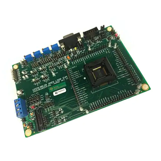
The UCD3138A64OEVM-662 EVM offers an easy to use test platform for stand-alone evaluation of
UCD3138A64 digital controller optimized for isolated power applications. Featuring an 80-pin socket
and a comprehensive set of test points, the EVM allows hardware and firmware engineers to
manipulate signals on the different pins of the device individually and study open loop operation. The
EVM also offers the flexibility to realize simple closed loop control configurations (eg. using RC
circuits to filter PWM output signals and regulate a DC voltage in closed loop control). Hardware
ports available to communicate with the device include PMBus and UART. The EVM accepts up to
5V DC input and an on-board 3.3V LDO can be used to bias the device. Alternately, using jumpers,
the device can be biased using the PMBus communication pins.
NOTE: In order to download firmware and program the UCD3138A64 device in
UCD3138A64OEVM-662, a separate EVM from Texas Instruments known as the USB-TO-GPIO
Adapter is required. The USB-TO-GPIO Adapter is NOT supplied with UCD3138A64OEVM-662 and
must be purchased separately. The USB-TO-GPIO Adapter serves as a communication interface
adaptor or a bridge between a host PC and the UCD3138A64 via a standard type-A to mini-B USB
cable. The USB-TO-GPIO Adapter is listed below in the related products section.
2
Description
UCD3138A64OEVM-662 is an EVM board to facilitate evaluation on UCD3138A64PFC digital power
controller. This EVM provides hardware needed to evaluate UCD3138A64 80-pin device. All pins of
UCD3138A64PFC are accessible through header connections, including all GPIO pins, ADC12 pins,
front end pins, DPWM pins, and Fault pins, etc. Particularly, the board has terminal of PMBus,
UART DB-9 RS232, and JTAG. All headers can be jumped to configure for a particular interested
evaluation need.
2.1
Typical Applications
2.2
UCD3138A64 function evaluation
Firmware debug
Hardware design assistance
Features
Test points for easy access to all pins of UCD3138A64 80-pin digital controller
Socket for easy removal/replacement of the device
All GPIO and ADC12 pins accessible (with on-board RC filters on each pin)
Capability to adapt EVM for various evaluation targets using jumpers
Hardware terminals: PMBus, UART, and Logic Analyzer
Includes On-board SPI and I2C accessible EEPROMs for additional memory storage
External 5.0V supply input with onboard 3.3V LDO to bias the device (option to bias device
using PMBus port)
LED indicators
Rich test points to facilitate the IC evaluation, system design and circuit and firmware debugging
Board with jumpers to make flexible configuration to adapt various evaluation target
Using the UCD3138A64OEVM-662
4
�SLUUB73
3
Specifications
Table 1.
Parameter
Connector J21
J21-4
J21-3
J21-2
J21-1
Connector J26
UART
Connector J27
JTAG
Connector J28
UCD3138A64OEVM-662 Specifications
Notes & Conditions
Min
Nom
3.45
5.10
3.33
Units
Port to use on board 3.3V to bias external circuit
External +5.0V to board
External +3.3V to board
Digital ground DGND
3.25
4.90
3.27
Female DB-9, RS232
Standard
Standard JTAG communication connection
Standard
PMBus connector
Port of connection to USB-to-GPIO, Jump across
J56 (2&3) and J57 (2&3) to enable communication
to UCD3138A64 device. For pin definition, refer to
TI standard USB-to-GPIO document SLLU093
Standard
Operation Environment
Operating Temperature Range
MECHANICAL CHARACTERSTICS
Natural Convection
25
°C
Dimensions
Width
Length
Highest Component Height
4.0
6.0
0.512
in
in
in
Firmware for Testing
Filename
3.30
5.00
3.30
Max
VDC
VDC
VDC
PWR662_HelloWorld.x0
Using the UCD3138A64OEVM-662
5
�SLUUB73
4
Schematics
Figure 1.
UCD3138A64OEVM-662 Schematics (Socket) 1 of 10
Using the UCD3138A64OEVM-662
6
�SLUUB73
Figure 2.
UCD3138A64OEVM-662 Schematics (Headers) 2 of 10
Using the UCD3138A64OEVM-662
7
�SLUUB73
Figure 3.
UCD3138A64OEVM-662 Schematics (Filters) 3 of 10
Using the UCD3138A64OEVM-662
8
�SLUUB73
Figure 4.
UCD3138A64OEVM-662 Schematics (Bias and LEDs) 4 of 10
Using the UCD3138A64OEVM-662
9
�SLUUB73
Figure 5.
UCD3138A64OEVM-662 Schematics (UART and JTAG) 5 of 10
Using the UCD3138A64OEVM-662
10
�SLUUB73
Figure 6.
UCD3138A64OEVM-662 Schematics (PMBus) 6 of 10
Using the UCD3138A64OEVM-662
11
�SLUUB73
Figure 7.
UCD3138A64OEVM-662 Schematics (DPWM) 7 of 10
Using the UCD3138A64OEVM-662
12
�SLUUB73
Figure 8.
UCD3138A64OEVM-662 Schematics (EADC and ADC12) 8 of 10
Using the UCD3138A64OEVM-662
13
�SLUUB73
Figure 9.
UCD3138A64OEVM-662 Schematics (Misc) 9 of 10
Using the UCD3138A64OEVM-662
14
�SLUUB73
Figure 10. UCD3138A64OEVM-662 Schematics (Hardware) 10 of 10
Using the UCD3138A64OEVM-662
15
�SLUUB73
5
Test Equipment
5.1
PC Computer
5.1.1 Operating System
Microsoft Windows XP (32-bit), or Vista (32-bit), or Windows 7 (32-bit).
5.2
USB-to-GPIO Interface Adapter
This adapter is to establish the communication between the control card UCC3138A64OEVM-662
and the PC computer through the PMBus and the GUI, Texas Instruments Fusion Digital Power
Designer.
5.2.1 USB-to-GPIO Interface Adapter (HPA172)
Accessories including:
a)
USB interface adapter (HPA172)
b)
USB cable, 5 pin B Mini Male to Type A Male.
c)
Ribbon cable, socket to socket, 10 pin, 2 headers, polarized.
Figure 11. USB-to-GPIO Interface Adapter (HPA172) Outlook.
5.3
Oscilloscope
An oscilloscope of analog or digital type is capable of 200MHz bandwidth with Tektronix P6138 or
equivalent oscilloscope probe.
Using the UCD3138A64OEVM-662
16
�SLUUB73
6
Equipment Setup
6.1
GUI (Graphical User Interface)
6.1.1 File for Installation
The GUI installation file is TI-Fusion-Digital-Power-Designer-Version-1.9.54.exe or newer version.
Obtain the latest version of GUI from http://www.ti.com/tool/fusion_digital_power_designer.
6.1.2 Installation
Double click and launch the .exe file to start the installation. Click Next on the subsequent dialog
windows. When present, click I accept the agreement after reading it, then click Install. After the
installation, click Finish to exit setup, then click Exit Program.
6.1.3 Launch UCD3138 Device GUI
The GUI for UCD3138A64OEVM-662 board is launched with the following steps:
Click the Windows Start → click All Programs → click Texas Instruments Fusion Digital Power
Designer → click Device GUIs → click UCD3xxx and UCD9xxx Device GUI.
6.2
Hardware Setup
6.2.1 Setup Overview
Figure 11 shows the connection between UCD3138A64OEVM-662 and the PC computer through
USB-to-GPIO Interface Adapter.
USB Adapter Connection
a)
Connect one end of the ribbon cable to the EVM, and connect the other end to the USB
interface adapter
b)
Connect the Mini connector of the USB cable to the USB interface adapter, and connect the
other end to the USB port of the PC computer.
Using the UCD3138A64OEVM-662
17
�SLUUB73
Figure 12. UCD3138A64OEVM-662 Test Connections
Figure 13. UCD31xx Device GUI
Using the UCD3138A64OEVM-662
18
�SLUUB73
Figure 14. Firmware code downloading
Using the UCD3138A64OEVM-662
19
�SLUUB73
6.3
List of Test Points
Table 2.
The functions of each test point
Test Points
Name
Description
TP1, TP3, TP4, TP5,
TP10, TP12, TP15,
TP25, TP28, TP29
DGND
Digital Ground (for less sensitive / noisy signals)
TP2, TP9, TP11, TP20
AGND
Analog Ground (for more sensitive / less noisy signals)
TP6, TP8
V33D
Digital 3.3VDC
TP7
V33A
Analog 3.3VDC
TP13
UART J26-2
UART Transmitting
TP14
UART J26-3
UART Receiving
TP16
FLTR_DPWM0
DPWM0 Front End Connection
TP17
FLTR_DPWM1
DPWM1 Front End Connection
TP18
FLTR_DPWM2
DPWM2 Front End Connection
TP19
FLTR_DPWM3
DPWM3 Front End Connection
TP21
Q3 and Q4 Drain
Ramp generator
TP22
Q3 gate
Ramp generator
TP23
Q4 gate
Ramp generator
TP24
FFC_adj
Feed Forward Control Adjustment
J2, J3, J4, J5, J6, J7, J8,
J9
Device Pins
UCD3138A84 Pinout Headers
J11, J12, J13, J14
Fault Connections
Place jumper to choose to pull corresponding Fault pin to V33D,
DGND, or neither
J15
AD00 ADDR / FLTR
Place jumper to choose to filter AD00, or use it to create an address,
or neither
J16
AD01 ADDR / FLTR
Place jumper to choose to filter AD01, or use it to create an address,
or neither
J17, J20, J21, J22
Board Bias Power Management
J18
LED D1
Place jumper to choose connection to either GPIOA, GPIOB, or
neither.
J19
LED D2
Place jumper to choose connection to either GPIOA, GPIOB, or
neither.
J23
UART RX
Place jumper to use UART connector to communicate with UART
Module 0, or Module 1, of the UCD3138A64
J24
Logic Analyzer
Logic Analyzer connector, not populated
J25
UART TX
Place jumper to use UART connector to communicate with UART
Module 0, or Module 1, of the UCD3138A64
J26
UART
UART Connector, DB-9, Female, RS232
J27
JTAG
JTAG Connector Header
J28
PMBus
PMBus Connector
J29
PMBus CLK
Enables board side Pull-up Resistor. Jump to add 1.5kΩ Pull-up
resistor to PMBus Clocking line
J30
PMBus CTRL
Place jumper to connect PMBus Control Line
J31
PMBus DATA
Enables board side Pull-up Resistor. Jump to add 1.5kΩ Pull-up
resistor to PMBus Data line
J32
PMBus ALERT
Enables board side Pull-up Resistor. Jump to add 1.5kΩ Pull-up
resistor to PMBus ALERT line
Using the UCD3138A64OEVM-662
20
�SLUUB73
J33
DPWM0 Filter
DPWM Filter. Place Jumper to choose to filter DPWM0A or
DPWM0B in accordance with the schematic.
J34
DPWM1 Filter
DPWM Filter. Place Jumper to choose to filter DPWM1A or
DPWM1B in accordance with the schematic.
J35
DPWM2 Filter
DPWM Filter. Place Jumper to choose to filter DPWM2A or
DPWM2B in accordance with the schematic.
J36
DPWM3 Filter
DPWM Filter. Place Jumper to choose to filter DPWM3A or
DPWM3B in accordance with the schematic.
J37, J38, J39
EADC and DPWM
Place Jumpers to connect chosen filtered DPWM(s) to
EAP0S/EAP1S
J40, J41, J43, J46
ADC12
Place Jumpers to obtain intermediate voltage on select ADC12 pins.
J42
FFCS
Feed Forward Control Selection
J44, J45
FFC
Voltage Feed Forward Test Circuit
J47
Logic Connector
Header
Used to connect select signals to logic connector header.
J48, J49, J51, J53
SPI EEPROM
Place jumpers to connect SPI EEPROM to SPI MISO, MOSI, CLK,
and CS pins of UCD3138A64 device.
J50, J52
I2C EEPROM
Place jumpers to connect I2C EEPROM to I2C CLK and DATA pins
of UCD3138A64 device.
J56, J57
PMBus / I2C
Place jumpers to choose the PMBus connector’s connection to the
UCD3138A64 device. Connect to I2C pins, or PMBus pins.
S1
/RESET
Push button to reset UCD3138A64.
7
Test Procedure
7.1
Connection Test
1. Connect one end of the USB cable to the PC computer and the other end to the USB interface adapter,
HPA172. The LED on HPA172 should light up.
2. Connect HPA172 to PWR662 PMBus connector J28 with the ribbon cable. Jump across J22,
J56(2&3), and J57(2&3). LED D3 on PWR662 should light up.
3. Launch the GUI by the steps described in 5.1.3. Wait until the window in Figure 13 is shown.
4. Click “Scan Device in ROM Mode”, then wait and check Figure 13 on its “Log” and confirm “Found
ROM v1 IC v6 – UCD31xx A64 Rev 1”. If “Found ROM” not shown, Click “Device ID” then click
“Command Program to jump to ROM (sendByte0xD9) and then click “Scan Device in ROM Mode”
again.
Using the UCD3138A64OEVM-662
21
�SLUUB73
Figure 15 Using the UCD3xxx / UCD9xxx Device GUI Main Window
7.2
ADC12 Input Setup
5.
6.
7.
8.
9.
Connect a voltmeter with its positive terminal to J41-1 and return terminal to TP25.
Adjust R57 to make the voltage meter read 250mV +/- 0.1mV
Move the voltmeter positive terminal to J43-1.
Adjust R59 to make the voltmeter read 250mV +/- 0.1mV
Remove J22, and move the voltmeter positive terminal to J39 pin 1, and the negative terminal to J37
pin 1. Set the voltmeter to resistance, and tune the potentiometer R54, until the resistance is 4.07kohm
+/- 0.1kohm.
10. Remove the voltmeter probes, and re-connect the jumper across J22.
7.3
Communication Terminal using RS232 Serial Port
11. Set up Communication Terminal port settings as shown in Figure 16. Then save this setup as
“Test_UCD3138A64OEVM-662”. The detail how to set up UART terminal communication is addressed
in Appendix B.
12. Connect RS232 Serial Port (UART) with DB9 male to PWR662 J26 and DB9 female to PC. Jump
across J23(2&3) and J25(2&3).
13. Launch saved terminal.
Using the UCD3138A64OEVM-662
22
�SLUUB73
Figure 16 Terminal Communication Settings
Figure 17: Download the Firmware
7.4
Setup-A Test
14. Place jumpers on the following Headers:
J18(1&2) and J19(1&2)
J27(11&13)
J11(1&2), J12(1&2), J13(1&2), and J14(1&2).
Using the UCD3138A64OEVM-662
23
�SLUUB73
15.
16.
17.
18.
19.
J16(1&2), J46(2&3), J43(1&2)(3&4)(5&6)(7&8)(9&10)(11&12)(13&14), J41(13&14)
J48, J49, J51, and J53
J50
J38(1&2)(3&4)(5&6)(7&8), J37, J39, J33(2&3), J34(2&3), J35(2&3), and J36(2&3)
Using clip wires, short PWM0,1,2,3, TCAP0, TCAP1, INT_EXT, SYNC, and ADC_EXT_TRIG to V33D.
That is, J6pins1,2,3,4, J9pins4,9,10, and J7pins2,9 must all be shorted together and connected to
TP6.
On the GUI shown in Figure 15, click Firmware Download, then a new window should come up as in
Figure 17. On this new window,
a) Check “Download data flash”, “DO NOT write program checksum”, and “Block 0 (32kB)” as
shown in Figure 17
b) Click “Select file” and find “PWR662_Test.x0”. Click “Download”.
c) When asked, “Do you want to continue with the firmware download?”, click “Yes” to continue.
After finishing the program download, the PWR662 board starts self-test automatically. The test status
is reported by the Hyper Terminal, shown in Figure 18. With Setup-A, Tests A1-A8 should pass.
Check LED D1 and D2. Both should light up.
Click “Close” to close the Firmware Download window shown in Figure 17.
Using the UCD3138A64OEVM-662
24
�SLUUB73
Figure 18: Setup-A Test Result
7.5
Equipment Shutdown
a. Exit the GUI and UART
b. Disconnect the cables.
8
EVM Assembly Drawing and PCB layout
The following figures (Figure 17 through Figure 22) show the design of the UCD3138A64OEVM-662
printed circuit board. PCB dimensions: L x W = 6.0 x 4.0 in, PCB material: FR4 or compatible, four
layers and 1oz copper on each layer.
Using the UCD3138A64OEVM-662
25
�SLUUB73
Figure 15. UCD3138A64OEVM-662 Top Layer Assembly Drawing (Top view)
Figure 16. UCD3138A64OEVM-662 Bottom Assembly Drawing (Bottom view)
Using the UCD3138A64OEVM-662
26
�SLUUB73
Figure 17. UCD3138A64OEVM-662 Top Copper (Top View)
Figure 18. UCD3138A64OEVM-662 Internal Layer 1 (Top View)
Using the UCD3138A64OEVM-662
27
�SLUUB73
Figure 19. UCD3138A64OEVM-662 Internal Layer 2 (Top View)
Figure 20. UCD3138A64OEVM-662 Bottom Copper (Top View)
Using the UCD3138A64OEVM-662
28
�SLUUB73
9
Bill of Materials
Table 3.
The EVM components list according to the schematics shown in Figure 1 to 10
RefDes
Q
TY
!PCB
1
C3
1
0.1uF
CAP, CERM, 0.1uF, 16V, +/-10%,
X7R, 0603
C5, C7, C11, C13,
C16, C36, C37
7
1000p
F
C6, C8, C12, C14
4
C9
Value
Description
Size
Part Number
MFR
PWR662
Any
0603
C0603C104K4RACTU
Kemet
CAP, CERM, 1000pF, 50V, +/-5%,
C0G/NP0, 0603
0603
C0603C102J5GAC
Kemet
4.7uF
CAP, CERM, 4.7uF, 16V, +/-10%,
X5R, 0603
0603
GRM188R61C475KAAJ
MuRata
1
0.1uF
CAP, CERM, 0.1uF, 25V, +/-10%,
X5R, 0603
0603
GRM188R61E104KA01D
MuRata
C15, C39, C42, C49
4
1uF
CAP, CERM, 1uF, 16V, +/-10%, X7R,
0603
0603
GRM188R71C105KA12D
MuRata
C17
1
0.1uF
CAP, CERM, 0.1uF, 25V, +/-10%,
X7R, 0603
0603
GRM188R71E104KA01D
MuRata
C18, C19, C20, C22,
C23, C24, C26, C27,
C28, C30, C31, C32,
C33, C34, C35
15
1000p
F
CAP, CERM, 1000pF, 50V, +/-10%,
X7R, 0603
0603
GRM188R71H102KA01D
MuRata
C21, C25, C29
3
100pF
CAP, CERM, 100pF, 50V, +/-5%,
C0G/NP0, 0603
0603
GRM1885C1H101JA01D
MuRata
C38, C40, C41
3
10uF
CAP, TA, 10uF, 10V, +/-20%, 3.4
ohm, SMD
3216-18
293D106X0010A2TE3
Vishay-Sprague
C43, C44, C45, C46,
C47, C56, C57, C58,
C59, C60, C61
11
0.1uF
CAP, CERM, 0.1uF, 16V, +/-10%,
X7R, 0603
0603
GRM188R71C104KA01D
MuRata
C48, C50, C52, C53,
C54, C55
6
1000p
F
CAP, CERM, 1000pF, 50V, +/-10%,
X7R, 0603
0603
C0603C102K5RACTU
Kemet
D1
1
Orang
e
LED, Orange, SMD
1.6x0.8x0.8
mm
LTST-C190KFKT
Lite-On
LTST-C190CKT
Lite-On
Printed Circuit Board
D2
1
Red
LED, Red, SMD
Red LED,
1.6x0.8x0.8
mm
D3
1
Green
LED, Green, SMD
1.6x0.8x0.8
mm
LTST-C190GKT
Lite-On
D4, D5
2
5.1V
Diode, Zener, 5.1V, 300mW, SOT-23
SOT-23
AZ23C5V1-7-F
Diodes Inc.
H1, H2, H3, H4
4
Machine Screw, Round, #4-40 x 1/4,
Nylon, Philips panhead
Screw
NY PMS 440 0025 PH
B&F Fastener
Supply
H5, H6, H7, H8
4
Standoff, Hex, 0.5"L #4-40 Nylon
Standoff
1902C
Keystone
J2, J3, J4, J5, J6, J7,
J8, J9
8
Header, TH, 100mil, 10x1, Gold
plated, 230 mil above insulator
10x1
Header
TSW-110-07-G-S
Samtec
Using the UCD3138A64OEVM-662
29
�SLUUB73
J11, J12, J13, J14,
J15, J16, J18, J19,
J20, J23, J25, J33,
J34, J35, J36, J44,
J46, J56, J57
PEC03SAAN
Sullins
Connector
Solutions
Header, 100mil, 2x1, Tin plated, TH
Header, 2
PIN, 100mil,
Tin
PEC02SAAN
Sullins
Connector
Solutions
1
TERMINAL BLOCK 5.08MM VERT
4POS, TH
TERM_BLK,
4pos,
5.08mm
ED120/4DS
On-Shore
Technology
1
CONN DB9 FEMALE R/A SOLDER
TH
D-SUB 9
PIN
182-009-213R171
NorComp
3
Header, 100mil, 7x2, Tin plated, TH
Header,
7x2, 100mil,
Tin
PEC07DAAN
Sullins
Connector
Solutions
1
Header (shrouded), 100mil, 5x2, HighTemperature, Gold, TH
5x2
Shrouded
header
N2510-6002-RB
3M
PEC04DAAN
Sullins
Connector
Solutions
Header, 100mil, 3x1, Tin plated, TH
Header, 3
PIN, 100mil,
Tin
17
J21
J26
J17, J22, J29, J30,
J31, J32, J37, J39,
J40, J42, J45, J48,
J49, J50, J51, J52,
J53
J27, J41, J43
J28
19
J38
1
Header, 100mil, 4x2, Tin plated, TH
Header,
4x2, 100mil,
Tin
J47
1
Header, TH, 100mil, 4x1, Gold plated,
230 mil above insulator
4x1 Header
TSW-104-07-G-S
Samtec
NT1
1
Single point connection between nets.
Q1, Q2
2
0.2V
Transistor, NPN, 40V, 0.2A, SOT-23
SOT-23
MMBT3904
Fairchild
Semiconductor
Q3, Q4
2
60V
MOSFET, N-CH, 60V, 0.17A, SOT-23
SOT-23
2N7002-7-F
Diodes Inc.
R1, R58, R64
3
1.0k
RES, 1.0k ohm, 5%, 0.1W, 0603
0603
CRCW06031K00JNEA
Vishay-Dale
R2, R3
2
4.7k
RES, 4.7k ohm, 5%, 0.1W, 0603
0603
CRCW06034K70JNEA
Vishay-Dale
R4, R5, R6, R7, R32,
R33, R37, R38, R39,
R40, R41, R42, R55,
R56, R61, R62, R63
17
10.0k
RES, 10.0k ohm, 1%, 0.1W, 0603
0603
CRCW060310K0FKEA
Vishay-Dale
R8, R9, R10, R12,
R13, R14, R16, R17,
R18, R20, R21, R22,
R23, R24, R25
15
100
RES, 100 ohm, 1%, 0.1W, 0603
0603
CRCW0603100RFKEA
Vishay-Dale
R11, R15, R19
3
1.00k
RES, 1.00k ohm, 1%, 0.1W, 0603
0603
CRCW06031K00FKEA
Vishay-Dale
R26
1
44.2k
RES, 44.2k ohm, 1%, 0.1W, 0603
0603
CRCW060344K2FKEA
Vishay-Dale
R27
1
22.6k
RES, 22.6k ohm, 1%, 0.1W, 0603
0603
CRCW060322K6FKEA
Vishay-Dale
R28, R29
2
100
RES, 100 ohm, 1%, 0.125W, 0805
0805
CRCW0805100RFKEA
Vishay-Dale
R30, R31
2
4.70k
RES, 4.70k ohm, 1%, 0.1W, 0603
0603
RC0603FR-074K7L
Yageo America
R34
1
0
RES, 0 ohm, 5%, 0.333W, 0805
0805
CRCW08050000Z0EAHP
Vishay-Dale
Using the UCD3138A64OEVM-662
30
�SLUUB73
R35
1
200
RES, 200 ohm, 5%, 0.1W, 0603
0603
CRCW0603200RJNEA
Vishay-Dale
R36
1
0
RES, 0 ohm, 5%, 0.1W, 0603
0603
CRCW06030000Z0EA
Vishay-Dale
R43, R47, R49
3
1.5k
RES, 1.5k ohm, 5%, 0.1W, 0603
0603
CRCW06031K50JNEA
Vishay-Dale
R44, R45, R46, R48
4
33
RES, 33 ohm, 5%, 0.1W, 0603
0603
CRCW060333R0JNEA
Vishay-Dale
R50, R51, R52, R53
4
2.00k
RES, 2.00k ohm, 1%, 0.1W, 0603
0603
CRCW06032K00FKEA
Vishay-Dale
R54, R57, R59, R60
4
20k
ohm
TRIMMER, 20K, 0.5W, TH
9.5x10x4.8
mm
3296Y-1-203LF
Bourns
Switch, Tactile, SPST-NO, 1VA, 32V,
SMT
Switch,
6.3x5.36x6.
6 mm, SMT
KT11P2JM34LFS
C&K
Components
Shunt, 100mil, Flash Gold, Black
Closed Top
100mil
Shunt
SPC02SYAN
Sullins
Connector
Solutions
Test Point, Multipurpose, Black, TH
Black
Multipurpos
e Testpoint
5011
Keystone
5128
Keystone
S1
SH-J1, SH-J2, SHJ3, SH-J4, SH-J5,
SH-J6, SH-J7, SHJ8, SH-J9, SH-J10,
SH-J11
TP1, TP5, TP15
1
11
3
1x2
Black
TP2
1
Grey
Test Point, Multipurpose, Grey, TH
Grey
Multipurpos
e Testpoint
TP3, TP4, TP9,
TP10, TP11, TP12,
TP20, TP25, TP28,
TP29
10
Triple
Terminal, Turret, TH, Triple
Keystone15
98-2
1598-2
Keystone
Test Point, Multipurpose, Red, TH
Red
Multipurpos
e Testpoint
5010
Keystone
Test Point, Multipurpose, Orange, TH
Orange
Multipurpos
e Testpoint
5013
Keystone
Test Point, Miniature, White, TH
White
Miniature
Testpoint
5002
Keystone
Test Point, Miniature, Yellow, TH
Yellow
Miniature
Testpoint
5004
Keystone
TP6, TP8
TP7
TP13, TP16, TP17,
TP18, TP19, TP21,
TP22, TP23, TP24
2
Red
1
Orang
e
9
White
TP14
1
U1
1
IC, EEPROM, 2MBIT, 1MHZ, 8SOIC
SOIC-8
M24M02-DRMN6TP
STMicroelectron
ics
1
2-Mbit DataFlash (with Extra 64Kbits), 1.65V Minimum SPI Serial
Flash Memory, SOIC-8
SOIC-8
AT45DB021E-SSHN-B
Adesto
Technologies
U3
1
LOW-POWER 150-mA LOWDROPOUT LINEAR REGULATOR,
DBV0005A
DBV0005A
TPS76333DBV
Texas
Instruments
U4
1
3-V to 5.5-V Single-Channel RS-232
Compatible Line Driver / Receiver, 0
DB0016A
SN75C3221DBR
Texas
Instruments
U2
Yellow
Using the UCD3138A64OEVM-662
31
�SLUUB73
to 70 degC, 16-Pin SSOP (DB),
Green (RoHS & no Sb/Br)
U5, U6, U7
3
Low-Noise, Low Quiescent Current,
Precision Operational Amplifier e-trim
Series, DBV0005A
U8
1
UCD3138A64PFC, PFC0080
PFC0080A
UCD3138A64PFC
Texas
Instruments
XU1
1
Socket, QFN-80, 0.5mm pitch, TH
29X16.5X29
mm
IC357-0804-074P-2
Yamaichi
Electronics
C1, C2
0
10pF
CAP, CERM, 10pF, 50V, +/-5%,
C0G/NP0, 0603
0603
C0603C100J5GACTU
Kemet
C4
0
2.2uF
CAP, CERM, 2.2uF, 10V, +/-10%,
X7R, 0603
0603
GRM188R71A225KE15D
MuRata
C51
0
1uF
CAP, CERM, 1uF, 16V, +/-10%, X7R,
0603
0603
GRM188R71C105KA12D
MuRata
FID1, FID2, FID3,
FID4, FID5, FID6
0
Fiducial mark. There is nothing to buy
or mount.
Fiducial
N/A
N/A
J24
0
CONN RECEPT 38POS .025 VERT
SMD
1000x250x2
72 mil
2-5767004-2
TE Connectivity
Y1
0
Crystal, 10.000MHz, 10pF, SMD
5x0.9x3.2m
m
7B-10.000MEEQ-T
TXC
Corporation
DBV0005A
OPA376AIDBV
Texas
Instruments
Using the UCD3138A64OEVM-662
32
�Appendix A. Using Code Composer Studio v5.5
In this appendix, the basic steps of how to use Code Composer Studio v5.5 to compile firmware
for UCD3138 family of devices is described. A design flow is described while detailed steps for
firmware code creation, and firmware debugging along with hardware are obviously beyond the
scope of this user’s guide and this appendix.
A.1
Importing a CCSv5 project
Upon running CCSv5.5 for the first time, the Workspace Launcher window will appear as
shown in Figure A1: CCSv5.5 Workspace Launcher. It is left to the user do decide whether or
not to use a workspace, where it is located, and/or to check the box that says Use this as the
default and do not ask again. For this guide, a workspace will not be used, so click OK.
Figure A1: CCSv5.5 Workspace Launcher
When the main window opens, click Project in the top navigation menu, then choose Import
Existing CCS Eclipse Project as shown in window as shown in Figure A2: Import Existing
CCS Eclipse Project.
�Figure A2: Import Existing CCS Eclipse Project
This will open the window shown in Figure A3: Importing a CCSv5.5 project. Under Selectsearch directory, click Browse, navigate to the target project, and click OK. For this example,
the project is called Training_CCSv5.5 and is located in a folder called Training_CCS5v5.
Check the box next to the discovered project, and do not check Copy projects into workspace,
or Automatically import referenced projects. Click Finish.
Figure A3: Importing a CCSv5.5 project
�The project should be imported into CCSv5.5 and should be shown in the Project Explorer as
shown in Figure A4: Project Explorer. At this point, files in the project can be edited as required.
Figure A4: Project Explorer
A.2
Build/Compile a Project using Code Composer Studio v5.5
For the UCD3138 family of devices, compiling a project produces an Intel-hex (.x0) firmware file that
can be downloaded to, and run on the UCD3138 or related target device using the UCD3XXX /
UCD9XXX Device GUI (part of the Fusion Design Online software from TI).
After finished editing the project files, Right-Click on the project in the Project explorer, and choose
Build Project.
Note: If this is the first time building a UCD3138 or related project, and Cygwin is also installed on the
PC that is performing the compilation, the instructions in Section 3.3 of the Application Note entitled
“Converting UCD3138 Firmware Project from Code Composer Studio Version 3.3 to 5.2” must be
followed. Mainly, the C:\CYGWIN or other similarly named directory must be renamed temporarily
during this first build. This will allow the new ARM library to be built properly. After this first build, the
CYGWIN directory can be rolled back to its original name, and future builds can compile successfully.
Builds may take up to a minute to compile, or longer for a first time build. Figure A5: Successful Build
of UCD3138 Related Source Code shows the state of a successful build:
�Figure A5: Successful Build of UCD3138 Related Source Code
When the build has finished, the .x0 file should be created and will be placed in the project directory’s
debug folder. The filename that prefaces the .x0 will be the name of the project that was built (i.e. a
project named Training_CCS5v5 will create Training_CCS5v5.x0 as its firmware file). However, it
must be noted that the project name must have no spaces, otherwise the .x0 file will not be generated.
This .x0 file can be and run on the UCD3138 target device using the UCD3XXX / UCD9XXX Device
GUI.
�Appendix B. Setting up PuTTY
PuTTY is an open source Telnet and SSH terminal software that can be downloaded from www.putty.org.
Download and run the putty.exe installation file. Follow the installation prompts making sure to allow the program to install
to the default directory.
Step 1
In Windows, launch from its installed directory using the start menu (StartProgramsPuTTYPuTTY)
Figure B1: Starting Putty
Step 2
On the main Session category, click the Serial radio button.
�Figure B2 Step 2
Step 3
Under the Connection category, click Serial as highlighted in the figure from Step 2. Configure the information as shown in
the image below. However, instead of COM1, use the serial line in which the Device Under Test (DUT) is connected on the
PC. Baud = 9600, Data bits = 8, Stop bits = 1, Parity = None, and Flow Control = XON/XOFF.
Figure B3 Step 3
�Step 4
Click back to the main Session category, and enter in a save name for this configuration such as PWR662_Test as shown
below. Click Save. This will save the session configuration so that upon closing and re-opening PuTTY, just click on the
saved session name, and choose Load.
Figure B4 Step 4
Step 5
Click Open to open the serial terminal session with the DUT.
�References
1.
2.
3.
4.
5.
6.
7.
8.
9.
10.
UCD3138A64 Data Manual (SLUSBZ8)
UCD3138 Monitoring and Communications Programmer’s Manual (SLUU996)
UCD3138 Digital Power Peripherals Programmer’s Manual (SLUU995)
UCD3138 ARM and Digital System Programmer’s Manual (SLUU994)
Fusion Digital Power Designer GUI for Isolated Power Applications User Guide (for UCD3138,
UCD3138064, UCD3138A64 applications) (SLUA676)
Code Composer Studio v5 Wiki, Texas Instruments,
http://processors.wiki.ti.com/index.php/Category:Code_Composer_Studio_v5
Converting UCD3138 Firmware Project from Code Composer Studio Version 3.3 to 5.2 (SLUA679)
UCD3138A64 Programmer’s Manual (SLUUB54)
UCD3138 Datasheet, SLUSAP2, 2012
UCD3138CC64EVM-030 Evaluation Module and User’s Guide, SLUU886, 2012
�EVALUATION BOARD/KIT/MODULE (EVM) WARNINGS, RESTRICTIONS AND DISCLAIMER
For Feasibility Evaluation Only, in Laboratory/Development Environments. The EVM is not a complete product. It is intended solely for use for
preliminary feasibility evaluation in laboratory / development environments by technically qualified electronics experts who are familiar with the dangers
and application risks associated with handling electrical / mechanical components, systems and subsystems. It should not be used as all or part of a
production unit.
Your Sole Responsibility and Risk. You acknowledge, represent and agree that:
1.
You have unique knowledge concerning Federal, State and local regulatory requirements (including but not limited to Food and Drug
Administration regulations, if applicable) which relate to your products and which relate to your use (and/or that of your employees, affiliates,
contractors or designees) of the EVM for evaluation, testing and other purposes.
2.
You have full and exclusive responsibility to assure the safety and compliance of your products with all such laws and other
applicable regulatory requirements, and also to assure the safety of any activities to be conducted by you and/or your employees, affiliates,
contractors or designees, using the EVM. Further, you are responsible to assure that any interfaces (electronic and/or mechanical) between the
EVM and any human body are designed with suitable isolation and means to safely limit accessible leakage currents to minimize the risk of
electrical shock hazard.
3.
Since the EVM is not a completed product, it may not meet all applicable regulatory and safety compliance standards (such as UL, CSA, VDE,
CE, RoHS and WEEE) which may normally be associated with similar items. You assume full responsibility to determine and/or assure
compliance with any such standards and related certifications as may be applicable. You will employ reasonable safeguards to ensure that your
use of the EVM will not result in any property damage, injury or death, even if the EVM should fail to perform as described or expected.
Certain Instructions.
Exceeding the specified EVM ratings (including but not limited to input and output voltage, current, power, and
environmental ranges) may cause property damage, personal injury or death. If there are questions concerning these ratings please contact a TI field
representative prior to connecting interface electronics including input power and intended loads. Any loads applied outside of the specified output range
may result in unintended and/or inaccurate operation and/or possible permanent damage to the EVM and/or interface electronics. Please consult the EVM
User’s Guide prior to connecting any load to the EVM output. If there is uncertainty as to the load specification, please contact a TI field representative.
During normal operation, some circuit components may have case temperatures greater than 60°C as long as the input and output ranges are maintained at
nominal ambient operating temperature. These components include but are not limited to linear regulators, switching transistors, pass transistors, and
current sense resistors which can be indentified using the EVM schematic located in the EVM User’s Guide. When placing measurement probes near these
devices during normal operation, please be aware that these devices may be very warm to the touch.
Agreement to Defend, Indemnify and Hold Harmless. You agree to defend, indemnify and hold TI, its licensors and their representatives harmless from
and against any and all claims, damages, losses, expenses, costs and liabilities (collectively, “Claims”) arising out of or in connection with any use of the
EVM that is not in accordance with the terms of this agreement. This obligation shall apply whether Claims arise under the law of tort or contract or any
other legal theory, and even if the EVM fails to perform as described or expected.
Safety-Critical or Life-Critical Applications. If you intend to evaluate TI components for possible use in safety-critical applications (such as life support)
where a failure of the TI product would reasonably be expected to cause severe personal injury or death, such as devices which are classified as FDA Class
III or similar classification, then you must specifically notify TI of such intent and enter into a separate Assurance and Indemnity Agreement.
�STANDARD TERMS AND CONDITIONS FOR EVALUATION MODULES
1.
Delivery: TI delivers TI evaluation boards, kits, or modules, including any accompanying demonstration software, components, or
documentation (collectively, an “EVM” or “EVMs”) to the User (“User”) in accordance with the terms and conditions set forth herein.
Acceptance of the EVM is expressly subject to the following terms and conditions.
1.1 EVMs are intended solely for product or software developers for use in a research and development setting to facilitate feasibility
evaluation, experimentation, or scientific analysis of TI semiconductors products. EVMs have no direct function and are not
finished products. EVMs shall not be directly or indirectly assembled as a part or subassembly in any finished product. For
clarification, any software or software tools provided with the EVM (“Software”) shall not be subject to the terms and conditions
set forth herein but rather shall be subject to the applicable terms and conditions that accompany such Software
1.2 EVMs are not intended for consumer or household use. EVMs may not be sold, sublicensed, leased, rented, loaned, assigned,
or otherwise distributed for commercial purposes by Users, in whole or in part, or used in any finished product or production
system.
2
Limited Warranty and Related Remedies/Disclaimers:
2.1 These terms and conditions do not apply to Software. The warranty, if any, for Software is covered in the applicable Software
License Agreement.
2.2 TI warrants that the TI EVM will conform to TI's published specifications for ninety (90) days after the date TI delivers such EVM
to User. Notwithstanding the foregoing, TI shall not be liable for any defects that are caused by neglect, misuse or mistreatment
by an entity other than TI, including improper installation or testing, or for any EVMs that have been altered or modified in any
way by an entity other than TI. Moreover, TI shall not be liable for any defects that result from User's design, specifications or
instructions for such EVMs. Testing and other quality control techniques are used to the extent TI deems necessary or as
mandated by government requirements. TI does not test all parameters of each EVM.
2.3 If any EVM fails to conform to the warranty set forth above, TI's sole liability shall be at its option to repair or replace such EVM,
or credit User's account for such EVM. TI's liability under this warranty shall be limited to EVMs that are returned during the
warranty period to the address designated by TI and that are determined by TI not to conform to such warranty. If TI elects to
repair or replace such EVM, TI shall have a reasonable time to repair such EVM or provide replacements. Repaired EVMs shall
be warranted for the remainder of the original warranty period. Replaced EVMs shall be warranted for a new full ninety (90) day
warranty period.
3
Regulatory Notices:
3.1 United States
3.1.1
Notice applicable to EVMs not FCC-Approved:
This kit is designed to allow product developers to evaluate electronic components, circuitry, or software associated with the kit
to determine whether to incorporate such items in a finished product and software developers to write software applications for
use with the end product. This kit is not a finished product and when assembled may not be resold or otherwise marketed unless
all required FCC equipment authorizations are first obtained. Operation is subject to the condition that this product not cause
harmful interference to licensed radio stations and that this product accept harmful interference. Unless the assembled kit is
designed to operate under part 15, part 18 or part 95 of this chapter, the operator of the kit must operate under the authority of
an FCC license holder or must secure an experimental authorization under part 5 of this chapter.
3.1.2
For EVMs annotated as FCC – FEDERAL COMMUNICATIONS COMMISSION Part 15 Compliant:
CAUTION
This device complies with part 15 of the FCC Rules. Operation is subject to the following two conditions: (1) This device may not
cause harmful interference, and (2) this device must accept any interference received, including interference that may cause
undesired operation.
Changes or modifications not expressly approved by the party responsible for compliance could void the user's authority to
operate the equipment.
FCC Interference Statement for Class A EVM devices
NOTE: This equipment has been tested and found to comply with the limits for a Class A digital device, pursuant to part 15 of
the FCC Rules. These limits are designed to provide reasonable protection against harmful interference when the equipment is
operated in a commercial environment. This equipment generates, uses, and can radiate radio frequency energy and, if not
installed and used in accordance with the instruction manual, may cause harmful interference to radio communications.
Operation of this equipment in a residential area is likely to cause harmful interference in which case the user will be required to
correct the interference at his own expense.
SPACER
SPACER
SPACER
SPACER
SPACER
SPACER
SPACER
SPACER
�FCC Interference Statement for Class B EVM devices
NOTE: This equipment has been tested and found to comply with the limits for a Class B digital device, pursuant to part 15 of
the FCC Rules. These limits are designed to provide reasonable protection against harmful interference in a residential
installation. This equipment generates, uses and can radiate radio frequency energy and, if not installed and used in accordance
with the instructions, may cause harmful interference to radio communications. However, there is no guarantee that interference
will not occur in a particular installation. If this equipment does cause harmful interference to radio or television reception, which
can be determined by turning the equipment off and on, the user is encouraged to try to correct the interference by one or more
of the following measures:
•
•
•
•
Reorient or relocate the receiving antenna.
Increase the separation between the equipment and receiver.
Connect the equipment into an outlet on a circuit different from that to which the receiver is connected.
Consult the dealer or an experienced radio/TV technician for help.
3.2 Canada
3.2.1
For EVMs issued with an Industry Canada Certificate of Conformance to RSS-210
Concerning EVMs Including Radio Transmitters:
This device complies with Industry Canada license-exempt RSS standard(s). Operation is subject to the following two conditions:
(1) this device may not cause interference, and (2) this device must accept any interference, including interference that may
cause undesired operation of the device.
Concernant les EVMs avec appareils radio:
Le présent appareil est conforme aux CNR d'Industrie Canada applicables aux appareils radio exempts de licence. L'exploitation
est autorisée aux deux conditions suivantes: (1) l'appareil ne doit pas produire de brouillage, et (2) l'utilisateur de l'appareil doit
accepter tout brouillage radioélectrique subi, même si le brouillage est susceptible d'en compromettre le fonctionnement.
Concerning EVMs Including Detachable Antennas:
Under Industry Canada regulations, this radio transmitter may only operate using an antenna of a type and maximum (or lesser)
gain approved for the transmitter by Industry Canada. To reduce potential radio interference to other users, the antenna type
and its gain should be so chosen that the equivalent isotropically radiated power (e.i.r.p.) is not more than that necessary for
successful communication. This radio transmitter has been approved by Industry Canada to operate with the antenna types
listed in the user guide with the maximum permissible gain and required antenna impedance for each antenna type indicated.
Antenna types not included in this list, having a gain greater than the maximum gain indicated for that type, are strictly prohibited
for use with this device.
Concernant les EVMs avec antennes détachables
Conformément à la réglementation d'Industrie Canada, le présent émetteur radio peut fonctionner avec une antenne d'un type et
d'un gain maximal (ou inférieur) approuvé pour l'émetteur par Industrie Canada. Dans le but de réduire les risques de brouillage
radioélectrique à l'intention des autres utilisateurs, il faut choisir le type d'antenne et son gain de sorte que la puissance isotrope
rayonnée équivalente (p.i.r.e.) ne dépasse pas l'intensité nécessaire à l'établissement d'une communication satisfaisante. Le
présent émetteur radio a été approuvé par Industrie Canada pour fonctionner avec les types d'antenne énumérés dans le
manuel d’usage et ayant un gain admissible maximal et l'impédance requise pour chaque type d'antenne. Les types d'antenne
non inclus dans cette liste, ou dont le gain est supérieur au gain maximal indiqué, sont strictement interdits pour l'exploitation de
l'émetteur
3.3 Japan
3.3.1
Notice for EVMs delivered in Japan: Please see http://www.tij.co.jp/lsds/ti_ja/general/eStore/notice_01.page 日本国内に
輸入される評価用キット、ボードについては、次のところをご覧ください。
http://www.tij.co.jp/lsds/ti_ja/general/eStore/notice_01.page
3.3.2
Notice for Users of EVMs Considered “Radio Frequency Products” in Japan: EVMs entering Japan may not be certified
by TI as conforming to Technical Regulations of Radio Law of Japan.
If User uses EVMs in Japan, not certified to Technical Regulations of Radio Law of Japan, User is required by Radio Law of
Japan to follow the instructions below with respect to EVMs:
1.
2.
3.
Use EVMs in a shielded room or any other test facility as defined in the notification #173 issued by Ministry of Internal
Affairs and Communications on March 28, 2006, based on Sub-section 1.1 of Article 6 of the Ministry’s Rule for
Enforcement of Radio Law of Japan,
Use EVMs only after User obtains the license of Test Radio Station as provided in Radio Law of Japan with respect to
EVMs, or
Use of EVMs only after User obtains the Technical Regulations Conformity Certification as provided in Radio Law of Japan
with respect to EVMs. Also, do not transfer EVMs, unless User gives the same notice above to the transferee. Please note
that if User does not follow the instructions above, User will be subject to penalties of Radio Law of Japan.
SPACER
SPACER
SPACER
SPACER
SPACER
�【無線電波を送信する製品の開発キットをお使いになる際の注意事項】 開発キットの中には技術基準適合証明を受けて
いないものがあります。 技術適合証明を受けていないもののご使用に際しては、電波法遵守のため、以下のいずれかの
措置を取っていただく必要がありますのでご注意ください。
1.
2.
3.
電波法施行規則第6条第1項第1号に基づく平成18年3月28日総務省告示第173号で定められた電波暗室等の試験設備でご使用
いただく。
実験局の免許を取得後ご使用いただく。
技術基準適合証明を取得後ご使用いただく。
なお、本製品は、上記の「ご使用にあたっての注意」を譲渡先、移転先に通知しない限り、譲渡、移転できないものとします。
上記を遵守頂けない場合は、電波法の罰則が適用される可能性があることをご留意ください。 日本テキサス・イ
ンスツルメンツ株式会社
東京都新宿区西新宿6丁目24番1号
西新宿三井ビル
3.3.3
Notice for EVMs for Power Line Communication: Please see http://www.tij.co.jp/lsds/ti_ja/general/eStore/notice_02.page
電力線搬送波通信についての開発キットをお使いになる際の注意事項については、次のところをご覧くださ
い。http://www.tij.co.jp/lsds/ti_ja/general/eStore/notice_02.page
SPACER
4
EVM Use Restrictions and Warnings:
4.1 EVMS ARE NOT FOR USE IN FUNCTIONAL SAFETY AND/OR SAFETY CRITICAL EVALUATIONS, INCLUDING BUT NOT
LIMITED TO EVALUATIONS OF LIFE SUPPORT APPLICATIONS.
4.2 User must read and apply the user guide and other available documentation provided by TI regarding the EVM prior to handling
or using the EVM, including without limitation any warning or restriction notices. The notices contain important safety information
related to, for example, temperatures and voltages.
4.3 Safety-Related Warnings and Restrictions:
4.3.1
User shall operate the EVM within TI’s recommended specifications and environmental considerations stated in the user
guide, other available documentation provided by TI, and any other applicable requirements and employ reasonable and
customary safeguards. Exceeding the specified performance ratings and specifications (including but not limited to input
and output voltage, current, power, and environmental ranges) for the EVM may cause personal injury or death, or
property damage. If there are questions concerning performance ratings and specifications, User should contact a TI
field representative prior to connecting interface electronics including input power and intended loads. Any loads applied
outside of the specified output range may also result in unintended and/or inaccurate operation and/or possible
permanent damage to the EVM and/or interface electronics. Please consult the EVM user guide prior to connecting any
load to the EVM output. If there is uncertainty as to the load specification, please contact a TI field representative.
During normal operation, even with the inputs and outputs kept within the specified allowable ranges, some circuit
components may have elevated case temperatures. These components include but are not limited to linear regulators,
switching transistors, pass transistors, current sense resistors, and heat sinks, which can be identified using the
information in the associated documentation. When working with the EVM, please be aware that the EVM may become
very warm.
4.3.2
EVMs are intended solely for use by technically qualified, professional electronics experts who are familiar with the
dangers and application risks associated with handling electrical mechanical components, systems, and subsystems.
User assumes all responsibility and liability for proper and safe handling and use of the EVM by User or its employees,
affiliates, contractors or designees. User assumes all responsibility and liability to ensure that any interfaces (electronic
and/or mechanical) between the EVM and any human body are designed with suitable isolation and means to safely
limit accessible leakage currents to minimize the risk of electrical shock hazard. User assumes all responsibility and
liability for any improper or unsafe handling or use of the EVM by User or its employees, affiliates, contractors or
designees.
4.4 User assumes all responsibility and liability to determine whether the EVM is subject to any applicable international, federal,
state, or local laws and regulations related to User’s handling and use of the EVM and, if applicable, User assumes all
responsibility and liability for compliance in all respects with such laws and regulations. User assumes all responsibility and
liability for proper disposal and recycling of the EVM consistent with all applicable international, federal, state, and local
requirements.
5.
Accuracy of Information: To the extent TI provides information on the availability and function of EVMs, TI attempts to be as accurate
as possible. However, TI does not warrant the accuracy of EVM descriptions, EVM availability or other information on its websites as
accurate, complete, reliable, current, or error-free.
SPACER
SPACER
SPACER
SPACER
SPACER
SPACER
�SPACER
6.
Disclaimers:
6.1 EXCEPT AS SET FORTH ABOVE, EVMS AND ANY WRITTEN DESIGN MATERIALS PROVIDED WITH THE EVM (AND THE
DESIGN OF THE EVM ITSELF) ARE PROVIDED "AS IS" AND "WITH ALL FAULTS." TI DISCLAIMS ALL OTHER
WARRANTIES, EXPRESS OR IMPLIED, REGARDING SUCH ITEMS, INCLUDING BUT NOT LIMITED TO ANY IMPLIED
WARRANTIES OF MERCHANTABILITY OR FITNESS FOR A PARTICULAR PURPOSE OR NON-INFRINGEMENT OF ANY
THIRD PARTY PATENTS, COPYRIGHTS, TRADE SECRETS OR OTHER INTELLECTUAL PROPERTY RIGHTS.
6.2 EXCEPT FOR THE LIMITED RIGHT TO USE THE EVM SET FORTH HEREIN, NOTHING IN THESE TERMS AND
CONDITIONS SHALL BE CONSTRUED AS GRANTING OR CONFERRING ANY RIGHTS BY LICENSE, PATENT, OR ANY
OTHER INDUSTRIAL OR INTELLECTUAL PROPERTY RIGHT OF TI, ITS SUPPLIERS/LICENSORS OR ANY OTHER THIRD
PARTY, TO USE THE EVM IN ANY FINISHED END-USER OR READY-TO-USE FINAL PRODUCT, OR FOR ANY
INVENTION, DISCOVERY OR IMPROVEMENT MADE, CONCEIVED OR ACQUIRED PRIOR TO OR AFTER DELIVERY OF
THE EVM.
7.
USER'S INDEMNITY OBLIGATIONS AND REPRESENTATIONS. USER WILL DEFEND, INDEMNIFY AND HOLD TI, ITS
LICENSORS AND THEIR REPRESENTATIVES HARMLESS FROM AND AGAINST ANY AND ALL CLAIMS, DAMAGES, LOSSES,
EXPENSES, COSTS AND LIABILITIES (COLLECTIVELY, "CLAIMS") ARISING OUT OF OR IN CONNECTION WITH ANY
HANDLING OR USE OF THE EVM THAT IS NOT IN ACCORDANCE WITH THESE TERMS AND CONDITIONS. THIS OBLIGATION
SHALL APPLY WHETHER CLAIMS ARISE UNDER STATUTE, REGULATION, OR THE LAW OF TORT, CONTRACT OR ANY
OTHER LEGAL THEORY, AND EVEN IF THE EVM FAILS TO PERFORM AS DESCRIBED OR EXPECTED.
8.
Limitations on Damages and Liability:
8.1 General Limitations. IN NO EVENT SHALL TI BE LIABLE FOR ANY SPECIAL, COLLATERAL, INDIRECT, PUNITIVE,
INCIDENTAL, CONSEQUENTIAL, OR EXEMPLARY DAMAGES IN CONNECTION WITH OR ARISING OUT OF THESE
TERMS ANDCONDITIONS OR THE USE OF THE EVMS PROVIDED HEREUNDER, REGARDLESS OF WHETHER TI HAS
BEEN ADVISED OF THE POSSIBILITY OF SUCH DAMAGES. EXCLUDED DAMAGES INCLUDE, BUT ARE NOT LIMITED
TO, COST OF REMOVAL OR REINSTALLATION, ANCILLARY COSTS TO THE PROCUREMENT OF SUBSTITUTE GOODS
OR SERVICES, RETESTING, OUTSIDE COMPUTER TIME, LABOR COSTS, LOSS OF GOODWILL, LOSS OF PROFITS,
LOSS OF SAVINGS, LOSS OF USE, LOSS OF DATA, OR BUSINESS INTERRUPTION. NO CLAIM, SUIT OR ACTION SHALL
BE BROUGHT AGAINST TI MORE THAN ONE YEAR AFTER THE RELATED CAUSE OF ACTION HAS OCCURRED.
8.2 Specific Limitations. IN NO EVENT SHALL TI'S AGGREGATE LIABILITY FROM ANY WARRANTY OR OTHER OBLIGATION
ARISING OUT OF OR IN CONNECTION WITH THESE TERMS AND CONDITIONS, OR ANY USE OF ANY TI EVM
PROVIDED HEREUNDER, EXCEED THE TOTAL AMOUNT PAID TO TI FOR THE PARTICULAR UNITS SOLD UNDER
THESE TERMS AND CONDITIONS WITH RESPECT TO WHICH LOSSES OR DAMAGES ARE CLAIMED. THE EXISTENCE
OF MORE THAN ONE CLAIM AGAINST THE PARTICULAR UNITS SOLD TO USER UNDER THESE TERMS AND
CONDITIONS SHALL NOT ENLARGE OR EXTEND THIS LIMIT.
9.
Return Policy. Except as otherwise provided, TI does not offer any refunds, returns, or exchanges. Furthermore, no return of EVM(s)
will be accepted if the package has been opened and no return of the EVM(s) will be accepted if they are damaged or otherwise not in
a resalable condition. If User feels it has been incorrectly charged for the EVM(s) it ordered or that delivery violates the applicable
order, User should contact TI. All refunds will be made in full within thirty (30) working days from the return of the components(s),
excluding any postage or packaging costs.
10. Governing Law: These terms and conditions shall be governed by and interpreted in accordance with the laws of the State of Texas,
without reference to conflict-of-laws principles. User agrees that non-exclusive jurisdiction for any dispute arising out of or relating to
these terms and conditions lies within courts located in the State of Texas and consents to venue in Dallas County, Texas.
Notwithstanding the foregoing, any judgment may be enforced in any United States or foreign court, and TI may seek injunctive relief
in any United States or foreign court.
Mailing Address: Texas Instruments, Post Office Box 655303, Dallas, Texas 75265
Copyright © 2015, Texas Instruments Incorporated
spacer
�IMPORTANT NOTICE
Texas Instruments Incorporated and its subsidiaries (TI) reserve the right to make corrections, enhancements, improvements and other
changes to its semiconductor products and services per JESD46, latest issue, and to discontinue any product or service per JESD48, latest
issue. Buyers should obtain the latest relevant information before placing orders and should verify that such information is current and
complete. All semiconductor products (also referred to herein as “components”) are sold subject to TI’s terms and conditions of sale
supplied at the time of order acknowledgment.
TI warrants performance of its components to the specifications applicable at the time of sale, in accordance with the warranty in TI’s terms
and conditions of sale of semiconductor products. Testing and other quality control techniques are used to the extent TI deems necessary
to support this warranty. Except where mandated by applicable law, testing of all parameters of each component is not necessarily
performed.
TI assumes no liability for applications assistance or the design of Buyers’ products. Buyers are responsible for their products and
applications using TI components. To minimize the risks associated with Buyers’ products and applications, Buyers should provide
adequate design and operating safeguards.
TI does not warrant or represent that any license, either express or implied, is granted under any patent right, copyright, mask work right, or
other intellectual property right relating to any combination, machine, or process in which TI components or services are used. Information
published by TI regarding third-party products or services does not constitute a license to use such products or services or a warranty or
endorsement thereof. Use of such information may require a license from a third party under the patents or other intellectual property of the
third party, or a license from TI under the patents or other intellectual property of TI.
Reproduction of significant portions of TI information in TI data books or data sheets is permissible only if reproduction is without alteration
and is accompanied by all associated warranties, conditions, limitations, and notices. TI is not responsible or liable for such altered
documentation. Information of third parties may be subject to additional restrictions.
Resale of TI components or services with statements different from or beyond the parameters stated by TI for that component or service
voids all express and any implied warranties for the associated TI component or service and is an unfair and deceptive business practice.
TI is not responsible or liable for any such statements.
Buyer acknowledges and agrees that it is solely responsible for compliance with all legal, regulatory and safety-related requirements
concerning its products, and any use of TI components in its applications, notwithstanding any applications-related information or support
that may be provided by TI. Buyer represents and agrees that it has all the necessary expertise to create and implement safeguards which
anticipate dangerous consequences of failures, monitor failures and their consequences, lessen the likelihood of failures that might cause
harm and take appropriate remedial actions. Buyer will fully indemnify TI and its representatives against any damages arising out of the use
of any TI components in safety-critical applications.
In some cases, TI components may be promoted specifically to facilitate safety-related applications. With such components, TI’s goal is to
help enable customers to design and create their own end-product solutions that meet applicable functional safety standards and
requirements. Nonetheless, such components are subject to these terms.
No TI components are authorized for use in FDA Class III (or similar life-critical medical equipment) unless authorized officers of the parties
have executed a special agreement specifically governing such use.
Only those TI components which TI has specifically designated as military grade or “enhanced plastic” are designed and intended for use in
military/aerospace applications or environments. Buyer acknowledges and agrees that any military or aerospace use of TI components
which have not been so designated is solely at the Buyer's risk, and that Buyer is solely responsible for compliance with all legal and
regulatory requirements in connection with such use.
TI has specifically designated certain components as meeting ISO/TS16949 requirements, mainly for automotive use. In any case of use of
non-designated products, TI will not be responsible for any failure to meet ISO/TS16949.
Products
Applications
Audio
www.ti.com/audio
Automotive and Transportation
www.ti.com/automotive
Amplifiers
amplifier.ti.com
Communications and Telecom
www.ti.com/communications
Data Converters
dataconverter.ti.com
Computers and Peripherals
www.ti.com/computers
DLP® Products
www.dlp.com
Consumer Electronics
www.ti.com/consumer-apps
DSP
dsp.ti.com
Energy and Lighting
www.ti.com/energy
Clocks and Timers
www.ti.com/clocks
Industrial
www.ti.com/industrial
Interface
interface.ti.com
Medical
www.ti.com/medical
Logic
logic.ti.com
Security
www.ti.com/security
Power Mgmt
power.ti.com
Space, Avionics and Defense
www.ti.com/space-avionics-defense
Microcontrollers
microcontroller.ti.com
Video and Imaging
www.ti.com/video
RFID
www.ti-rfid.com
OMAP Applications Processors
www.ti.com/omap
TI E2E Community
e2e.ti.com
Wireless Connectivity
www.ti.com/wirelessconnectivity
Mailing Address: Texas Instruments, Post Office Box 655303, Dallas, Texas 75265
Copyright © 2015, Texas Instruments Incorporated
�


 工商网监
湘ICP备2023018690号
工商网监
湘ICP备2023018690号
