Using the UCD3138LLCEVM-028
User's Guide
Literature Number: SLUU979A
August 2012 – Revised July 2013
�www.ti.com
WARNING
Always follow TI’s set-up and application instructions, including use of all interface components within their
recommended electrical rated voltage and power limits. Always use electrical safety precautions to help
ensure your personal safety and the safety of those working around you. Contact TI’s Product Information
Center http://support/ti./com for further information.
Save all warnings and instructions for future reference.
Failure to follow warnings and instructions may result in personal injury, property damage, or
death due to electrical shock and/or burn hazards.
The term TI HV EVM refers to an electronic device typically provided as an open framed, unenclosed
printed circuit board assembly. It is intended strictly for use in development laboratory environments,
solely for qualified professional users having training, expertise, and knowledge of electrical safety risks in
development and application of high-voltage electrical circuits. Any other use and/or application are strictly
prohibited by Texas Instruments. If you are not suitably qualified, you should immediately stop from further
use of the HV EVM.
1. Work Area Safety:
(a) Keep work area clean and orderly.
(b) Qualified observer(s) must be present anytime circuits are energized.
(c) Effective barriers and signage must be present in the area where the TI HV EVM and its interface
electronics are energized, indicating operation of accessible high voltages may be present, for the
purpose of protecting inadvertent access.
(d) All interface circuits, power supplies, evaluation modules, instruments, meters, scopes and other
related apparatus used in a development environment exceeding 50 VRMS/75 VDC must be
electrically located within a protected Emergency Power Off (EPO) protected power strip.
(e) Use a stable and non-conductive work surface.
(f) Use adequately insulated clamps and wires to attach measurement probes and instruments. No
freehand testing whenever possible.
2. Electrical Safety:
(a) De-energize the TI HV EVM and all its inputs, outputs, and electrical loads before performing any
electrical or other diagnostic measurements. Revalidate that TI HV EVM power has been safely deenergized.
(b) With the EVM confirmed de-energized, proceed with required electrical circuit configurations, wiring,
measurement equipment hook-ups and other application needs, while still assuming the EVM circuit
and measuring instruments are electrically live.
(c) Once EVM readiness is complete, energize the EVM as intended.
WARNING: while the EVM is energized, never touch the EVM or its electrical circuits as they
could be at high voltages capable of causing electrical shock hazard.
3. Personal Safety:
(a) Wear personal protective equipment e.g. latex gloves and/or safety glasses with side shields or
protect EVM in an adequate lucent plastic box with interlocks from accidental touch.
4. Limitation for Safe Use:
(a) EVMs are not to be used as all or part of a production unit.
2
SLUU979A – August 2012 – Revised July 2013
Submit Documentation Feedback
Copyright © 2012–2013, Texas Instruments Incorporated
�User's Guide
SLUU979A – August 2012 – Revised July 2013
Digitally Controlled LLC Resonant Half-Bridge DC-DC
Converter
1
Introduction
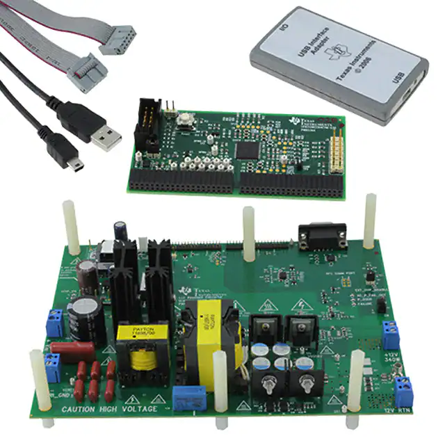
This EVM, UCD3138LLCEVM-028 is to help evaluate the UCD3138 64-pin digital control device in an offline power converter application and then to aid in its design. The EVM is a standalone LLC resonant halfbridge DC-to-DC power converter. The EVM is used together with its control card, UCD3138CC64EVM030, also an EVM on which is placed UCD3138RGC.
The UCD3138LLCEVM-028 together with UCD3138CC64EVM-030 can be used as they are delivered
without additional work, from either hardware or firmware, to evaluate an LLC resonant half-bridge DC-toDC converter. This EVM combination allows for some of its design parameters to be retuned using a GUI
based tool, called Texas Instruments Fusion Digital Power Designer. It is also possible to load custom
firmware with user’s own definition and development.
Three EVMs are included UCD3138LLCEVM-028, UCD3138CC64EVM-030, and USB-TO-GPIO.
This user’s guide provides basic evaluation instruction from a viewpoint of system operation in a
standalone LLC resonant half-bridge DC-to-DC power converter.
WARNING
• High voltages are present on this evaluation module during
operation and for a while even after power off. This module
should only be tested by skilled personnel in a controlled
laboratory environment.
• An isolated DC voltage source meeting IEC61010 reinforced
insulation standards is recommended for evaluating this EVM.
• High temperature exceeding 60°C may be found during EVM
operation and for a while even after power off.
• This EVM’s purpose is to facilitate the evaluation of digital
control in an LLC using the UCD3138, and cannot be tested
and treated as a final product.
• Extreme caution should be taken to eliminate the possibility of
electric shock and heat burn.
• Read and understand this user’s guide thoroughly before
starting any physical evaluation.
SLUU979A – August 2012 – Revised July 2013
Submit Documentation Feedback
Digitally Controlled LLC Resonant Half-Bridge DC-DC Converter
Copyright © 2012–2013, Texas Instruments Incorporated
3
�Description
2
www.ti.com
Description
The UCD3138LLCEVM-028 along with the UCD3138CC64EVM-030 demonstrates an LLC resonant halfbridge DC-DC power converter with digital control using the UCD3138 device. The UCD3138 device is
located on the UCD3138CC64EVM-030 board. The UCD3138CC64EVM-030 is a daughter card with
preloaded firmware that provides the required control functions for an LLC converter. For details of the
firmware please contact TI. UCD3138LLCEVM-028 accepts a DC input from 350 VDC to 400 VDC, and
outputs a nominal 12 VDC with full load output power of 340 W, or full output current of 29 A.
NOTE: This EVM does not have an input fuse and relies on the input current limit from the input
voltage source used.
2.1
Typical Applications
•
•
•
2.2
Features
•
•
•
•
•
•
•
•
•
•
•
•
•
•
4
Offline DC-to-DC Power Conversion
Servers
Telecommunication Systems
Digitally Controlled LLC Resonant Half-Bridge DC-to-DC Power Conversion
DC Input from 350 VDC to 400 VDC
12 VDC Regulated Output from No Load to Full Load
Full-Load Power 340 W, or Full-Load Current 29 A
High Efficiency
Constant Soft-Start Time
Protection: Over Voltage, Over Current, Brownout and Output Short-Circuit Protection
Test Points to Facilitate Device and Topology Evaluation
Synchronous Rectification
Automatic Mode Switching between LLC Mode and PWM Mode
Cycle-by-Cycle Current Limiting with Duty Cycle Matching
Constant Current and Constant Power Control Mode
PMBUS Communication
Current Sharing Capability (GUI Enable), Across Paralleled Units
Digitally Controlled LLC Resonant Half-Bridge DC-DC Converter
SLUU979A – August 2012 – Revised July 2013
Submit Documentation Feedback
Copyright © 2012–2013, Texas Instruments Incorporated
�Performance Specifications
www.ti.com
3
Performance Specifications
Table 1. UCD3138LLCEVM-028 Performance Specifications
PARAMETER
TEST CONDITIONS
MIN
TYP
MAX
UNITS
Input Characteristics
Voltage operation range
350
Input UVLO On
325
Input UVLO Off
310
400
VDC
A
Input current
Input = 350 VDC, full load = 29 A
1.2
Input current
Input = 380 VDC, full load = 29 A
1.1
Input current
Input = 400 VDC, full load = 29 A
1.0
Output Characteristics
Output voltage, VOUT
No load to full load
Output load current, IOUT
350 VDC to 400 VDC
12
Output voltage ripple
380 VDC and full load = 29 A
Output over current
Operation 10s then latch-off shutdown
30
Resonant mode
35
VDC
29
200
A
mVpp
A
Systems Characteristics
Switching frequency
PWM Mode
150
kHz
150
Peak efficiency
380 VDC, full load = 29 A
93.5%
Full-load efficiency
380 VDC, load = 20 A
94.0%
Operating temperature
Natural convection
25
ºC
Firmware
Device ID (version)
UCD3100ISO1 | 0.0.44.0000 | 120517
Filename
UCD3138LLCEVM_028_0_0_44_120517.x0
SLUU979A – August 2012 – Revised July 2013
Submit Documentation Feedback
Digitally Controlled LLC Resonant Half-Bridge DC-DC Converter
Copyright © 2012–2013, Texas Instruments Incorporated
5
�1
R38
10k
Copyright © 2012–2013, Texas Instruments Incorporated
1
DGND
R70
549
R71
100k
(J3-13)
10k
R72
R69
10k
R50
124
TP13
OUTB 5
VDD 6
OUTA 7
ENBB 8
4 INB
3 GND
2 INA
1 ENBA
10nF
C60
10
R67
12VS
C57
GATE 8
Diode Oring Control
7 GND
C 10
RSVD 9
5 OV
6 UV
A 11
FLTR 12
3 STAT
4 FLTB
BYP 13
PG 14
2 RSET
1 VDD
LSG
10
C58
C59
10nF
C61
100pF
9
10
6
2
5
1
C36
15nF
L1
33uH
1
R28
1k
C41
C38
C42
15nF
TP8
D12
TP19
+
C64
+
C65
+
2
1
C66
+
GND_PWR 1
SH1
+12V
100
R31
+
J6
R32
20k
1k
R33
Q5
Q4-A
R30
100
3_3VD
1 DGND
1
47uF 47uF
C69
47uF
1
SH2
47uF
C72
DGND
C71
1
R34
10k
Parts not used.
47uF
C70
Output Capacitors
(J2-35)
IO_SEN-
3m
3m
Load current sense
R77
R76
3m
R19
1
SH3
R22
1k
Q15
C73
1
4.7uF
1
1
Q14
SH4
AGND
C13
220pF
1
4
3
1
R18
1k
R12
1k
1k
R74
R73 - 74 Bleeder R's
TP20
R73
1k
TP2
HS4
AGND
0.1uF
C12
1
C62
0.1uF
1
C17
2200pF
(J2-39)
1 -VO_SENSE
C16
2200pF
1
Output Current Sense
35A scaled to 1.6V
(J2-38)
EADC_IOSENSE
IO_SENSE
(J2-30)
PWM0 (J3-25)
Current Share Compensation
AGND
R25
1k
AGND
R21
1k
1 12V_RTN
J12
+Vout Ripple Test
TP16
J11
Iout = 29A max
Pout = 340W max
+VOUT = +12VEXT
10nF
10k
10k
12V_RTN
R11
1
R24
R20
(J2-40, 10)
+VO_SENSE
TP12 SR_VDS2
Voltage Feedback
R49
1k
C14
R16
100 TP3
R13
549
1
Q11
IRLB3036GPbF
R48
+12VEXT
AGND
TP17
R23
35.7k
R15
549
U3
1
3_3VA
D7
SR2
HS3
+12VEXT
+12V
R14
549
C15
220pF
C11
0.1uF
TP14
SR1
AGND
OUTB 5
VDD 6
OUTA 7
35.7k
ORING_GATE
1mV/1A
R75
EXT_OVP_DISABLE
(J3-17)
4 INB
ENBB 8
1
GND_PWR
1
R47
Q10
IRLB3036GPbF
SR_VDS1
GND_PWR
R17
1k
1 ENBA
1 GND_PWR
(J2-36)
IO_SEN+
1
C45
0.1uF
HS5
U9
UCC27424DGN
3 GND
OUTB 5
Redundant OVP circuit.
C68
C44
2.2uF
2 INA
R58
10k
DPWM1A
(J3-3)
R46
1k
1
R45
IRLB3036GPbF
Q9
VDD 6
SR2
TP15
12VS
SR1
HS6
TP11
OUTA 7
ENBB 8
J6: short to disable Ext OVP
0.1uF
C26
+12V Q4-B
(J3-11)
4 INB
3 GND
2 INA
1 ENBA
U10
UCC27424DGN
GND_PWR
C52
0.1uF
1
R44
Q8
IRLB3036GPbF
1
GND_PWR
R29
20k
1
R64
10k
(J3-4)
DPWM1B
(J3-11)
OVLATCH
C51
2.2uF
SR gate drivers
OVLATCH
3,4
6
5
7,8
1
GND_PWR
C39
2.2nF
Isolation Line
470uF 470uF 470uF 470uF 470uF
TP18 C63
4
3
R42
5.11k
TP4
GND_PWR_PRI 1
R41
10
D11
1
2
T3
TRP2
TRP1
T2
1
GND_PWR_PRI
C32
0.1uF
R37
5.11k
D9
C27
0.1uF
15nF 15nF
+12V Monitoring and Protection
C20
2200pF
(J2-14)
R26
10k
C37
15nF
D13
R36
10
AGND
R27
100
R40
0
D10
R35
0
D8
15nF
C40
TP10
1
2
3
GND_PWR_PRI
VOSADC12
1:1:1
T1
HS2
6
5
4
HS1
GND_PWR_PRI
ORING_GATE
R68
5.11k
+12VEXT
C33 2.2uF
R39
1 GND_PWR
1
TP9
Q7
SPW20N60CFD
HSS
HSG
Q6
SPW20N60CFD
C29
0.1uF
100pF
+12V
GND_PWR
0.1uF
2.2uF
U11 2200pF
TPS2411PW
1
OUTB 5
VDD 6
OUTA 7
ENBB 8
C35
12VS
C28
2.2uF
C34
D15
BAT54S
D14
BAT54S
GND_PWR_PRI 1
U7
UCC27424DGN
1 GND_PWR
ORING_CTRL
R43
10k
4 INB
3 GND
2 INA
1 ENBA
BUS+_HV_PRI
+
C30
C31
47uF
1.5uF
U6
UCC27424DGN
(J3-11)
GND_PWR
DPWM0A
(J3-1)
R51
124
OVLATCH
1 AGND
C43
100pF
0.312V/A
DPWM0B
(J3-2)
R66
10k
IPS
(J2-12)
Primary Current Sense
J9
TP7
J8
+VIN = 350 to 400VDC.
Pin_max = 340W
TP5
PWPD
9
J10
PWPD
9
PWPD
Digitally Controlled LLC Resonant Half-Bridge DC-DC Converter
9
PWPD
9
6
5
4
2
VIN_HV_PRI
TP6
Schematics
www.ti.com
Schematics
Figure 1. UCD3138LLCEVM-028 Schematic (image 1 of 2)
SLUU979A – August 2012 – Revised July 2013
Submit Documentation Feedback
�Copyright © 2012–2013, Texas Instruments Incorporated
1
GND_PWR
D23
D22
D21
100pF
VAUX_P
0.1uF
C1
-VIN
-VAUX_-VIN
VAUX_P
VIN+
U1 PWR050
BUS+_HV_PRI
1
Isolation Line
DGND
D2
1
1
BAT54S
3_3VD
C3
2.2uF
R2
1
1
6
C4
0.1uF
7
U8-A
1
1
SRDET2
(J2-24)
J7
VIN_MON=1.93V AT VIN=400V
1
DGND
4 GND
3 NC
2 NC
FB/NC 5
NC 6
NC 7
OUT 8
1
3_3VD
OFF
SW1
5.11k
(J3-22)
ON/OFF
D3
R4
301
R3
1
AGND
10nF
C18
3_3VA
DGND
VO 3
C19
10nF
(J2-28)
TEMP
AGND
0.1uF
1
3_3VA
C6
1
1
Parts not used.
159.6 C - TEMP * 85.5 C/V
Temperature =
NC 1
GND 2
U4
LM20BIM7
5 GND
4 V+
C23
0.1uF
C24
0.1uF
1
D4
3_3VD
1
C25
0.1uF
0.1uF
FAILURE
(J3-34)
DGND
DGND
C21
GND 14
1
DGND
Q1
R6
301
P_GOOD
(J3-15)
D5
ROUT 9
8 RIN
(J3-24)SCI_RX1
(J3-23)SCI_TX1
INVALID 10
DIN 11
FORCEON 12
7 V-
6 C2-
5 C2+
DOUT 13
3 V+
4 C1-
VCC 15
FORCEOFF 16
U5
SN65C3221PW
2 C1+
1 EN
Q2
R7
301
Q3
D6
R8
301
AC_P_FAIL_OUT
(J3-26)
1
1
DGND
SCI Interface
V+ = +5.4V
V- = -5.4V
AGND
1 AGND
2 NC
3 AGND
4 AD00
5 AGND
6 AD01
7 AGND
8 AD02
9 AGND
10 AD03
11 AGND
12 AD04
13 AGND
14 AD05
15 AGND
16 AD06
17 AGND
18 AD07
19 AGND
20 AD08
21 AGND
22 AD09
23 AGND
24 AD10
25 AGND
26 AD11
27 AGND
28 AD12
29 AGND
30 AD13
31 AGND
32 NC
33 NC
34 NC
35 EAN2
36 EAP2
37 EAN1
38 EAP1
39 EAN0
40 EAP0
C22
0.1uF
DGND
3_3VD
DGND/AGND Damping
Control Card Connectors (PWR030)
J3
J2
DPWM0A
1 DPWM0A
2 DPWM0B
DPWM0B
3 DPWM1A
DPWM1A
4 DPWM1B
ADDRESS
DPWM1B
5 DPWM2A
DPWM2A
6 DPWM2B
(J2-4)
DPWM2B
7 DPWM3A
8 DPWM3B
9 DGND
10 DGND
C10
R10
11 FAULT0
OVLATCH
12 NC
1
1
ORING_CTRL
13 FAULT1
14 NC
P_GOOD
15 SYNC
16 NC
Device Address 1
17 FAULT2
EXT_OVP_DISABLE
18 NC
AGND
19 NC
20 NC
21 NC
22 FAULT3
ON/OFF
23 SCI_TX1
SCI_TX1
24 SCI_RX1
SCI_RX1
25 PWM_0
PWM0
26 PWM_1
AC_P_FAIL_OUT
I Share Bus
27 NC
28 NC
ISHARE
3
29 TCAP
30 NC
(J2-8)
2
31 SCI_TX0
SCI_TX0
32 SCI_RX0
SCI_RX0
C9
1
33 INT_EXT
AC_P_FAIL_IN
34 ADC_EXT
FAILURE
35 DGND
10nF
J4
36 /RESET
37 DGND
38 DGND
AGND
39 12V_EXT
12VS
40 3.3V
TP1
1
3_3VD
R5
10
DGND Test Point
AGND
DGND
DGND
1
1
1
Temperature Sensor
SCI_RX0 (J3-32)
SCI_TX0 (J3-31)
AC_P_FAIL_IN
(J3-33)
3.3VD LED Indicator
C7
1uF
DGND
ON
R9
On/off control
PFC Communication
1
3_3VD
C8
0.1uF
3_3VD
U2
TPS715A33DRBR
1 IN
C5
0.1uF
1
DGND
DGND
1
0.1uF
C2
1
AGND
0.01uF
1
AGND
1
C46
0.01uF
C53
10k
(J2-22)
SRDET1
External Power Input
J1
10k
C48
R56
1
R53
VIN_MON
(J2-6, 16)
1
1
C55
R63
1
R60
DGND
5
8
DGND
U8-B
2
1
AGND
C56
100pF
4
3
C49
100pF
1
GND_PWR
12VS
DGND
301
R65
R61
3.01k
DGND
Q12
R57
301
Q13
1
GND_PWR
GND
VIN_MONITOR
VAUX_S
C47
100pF
R59
1k
C54
3_3VD
GND_PWR_PRI
1
Bias power generation
VIN Operating Range: 300V to 400VDC.
12Vp_on
D1
R52
1k
1
(J3-6)
DPWM2B
Leading edge blanking pulse
D20
VAUX_P = +12V
R1
1.74k
GND_PWR
D19
D18
D17
(J3-5)
DPWM2A
Leading edge blanking pulse
51.1
51.1
R62
SR_VDS2
R55
D16
3
SR_VDS1
2
C50
0.1uF
1
R54
3.01k
9 PWPD
SR body diode conduction detection circuits
1
6
2
7
3
8
4
9
5
J5
IO_SENIO_SEN+
EADC_IOSENSE
-VO_SENSE
+VO_SENSE
IO_SENSE
TEMP
SRDET2
SRDET1
VIN_MON
VOSADC12
+VO_SENSE
IPS
ISHARE
ADDRESS
VIN_MON
10
SLUU979A – August 2012 – Revised July 2013
Submit Documentation Feedback
11
3_3VD
www.ti.com
Schematics
Figure 2. UCD3138PFCEVM-026 Schematic (image 2 of 2)
Digitally Controlled LLC Resonant Half-Bridge DC-DC Converter
7
�TP6
AD-12
AD-13
AD-10
AD-11
AD-09
DGND
/RESET
3.3VD
R29
R27
R21
1000pF
2K
2K
2K
R28
2K
AD-00
1
1
1
1
C18
1
TP10
C21
R24
R23
R19
C20
2K
100
100
100
EADC-N2
EADC-P2
R26
R25
R20
R18
100
100
100
100
C25
1
C22
TP24
1
1
1
TP22
1
TP23
C24
1
TP25
TP11
TP21
1
TP9
PMBUS-CLK
PMBUS-DATA
PMBUS-ALERT
PMBUS-CTRL
100
C23
1
TP8
R16
D2
BAT54A
EADC-P1
100
D1
BAT54A
100
EADC-N1
R17
EADC-N0
EADC-P0
R9
R8
100
100
PWM-0
C27
1
TP26
C17
33pF
PWM-1
C26
1
TP27
C29
1
TP28
C15
33pF
TP7
TP4
R14
1.5K
3.3VD
C28
C16
33pF
C2
1
C30
1
TP30
C1
C31
1
TP31
65
2
4
64
3
63
62
5
6
61
8
7
60
58
0.1uF
37
EAN2
EAP2
EAN1
EAP1
EAN0
EAP0
PWPD
AD10
AD11
AD12
AD13
AD08
AD09
AD07
AD06
AD05
AD02
AD03
AD04
AGND
RESET
TMS
1
NS1
24
23
22
21
35
29
43
42
SCI_RX1 30
SCI_TX1
FAULT3
FAULT1
36
FAULT2
FAULT0
26
12
SCI_RX0 13
SCI_TX0 14
SYNC
ADC_EXT
INT_EXT 34
DPWM3B
DPWM3A
DPWM2B
DPWM2A
20
18
17
41
11
40
39
DPWM1A 19
DPWM1B
DPWM0B
DPWM0A
U1
TCAP
UCD3138RGC
PMBUS_CLK
PMBUS_DATA
PMBUS_ALERT
TCK
TDO 38
TDI
PWM1
DGND
1
TCK
TP3
TCAP
DGND
1000pF
C8
16K
C7
100pF
DGND
TP2
DPWM-3B
DPWM-3A
DPWM-2B
DPWM-2A
DPWM-1B
DPWM-1A
DPWM-0B
DPWM-0A
R11
R10
10K
TP16
Parts not used
SCI-RX1
SCI-TX1
FAULT-3
FAULT-1
FAULT-2
FAULT-0
SCI-RX0
SCI-TX0
SYNC
EXT-TRIG
INT-EXT
TP20
TP17 TP18
TP14 TP15
TP12 TP13
/RESET
TMS
TDI
TDO
DGND
C12
DGND
1uF
2.2uF
TP19
3.3VD
C6
C11
0.1uF
C5
0.1uF
0.1uF
C4
PMBUS_CTRL
PWM0
AD01
59
AD00
55
54
53
52
51
50
15
16
27
28
32
31
AGND
1uF
DGND
33pF
33pF
TP29
C9
C10
R13
1.5K
0.1uF
1000pF 1000pF 1000pF 1000pF 1000pF 1000pF 1000pF 1000pF 1000pF 1000pF 1000pF 1000pF 1000pF 1000pF
C19
AD-03
AD-04
AD-05
AD-06
AD-07
AD-08
AD-02
R5
R7
DGND
AD-00
AD-01
0
R6
TP33 TP35 TP36
1
1
R22
TP32
R15
100K
DGND
J2
1
TP34
AGND
1
RESET
C14
C13
0.1uF
S1
1
2K
TP5
R12
1.65K
3.3VD
1
2
3
4
5
6
7
8
9
10
R4
57
V33A
R3
AGND
1
AGND
48
AGND
49
R2
47
V33D
C3
9
R1
56 AGND
J1
10
V33DIO
R39
45
V33DIO
DGND
44
DGND
33
TP1
46
BP18
DGND
Copyright © 2012–2013, Texas Instruments Incorporated
DGND
Digitally Controlled LLC Resonant Half-Bridge DC-DC Converter
10
8
25
3.3VA
Schematics
www.ti.com
Figure 3. UCD3138CC64EVM-030 Schematic (image 1 of 2)
SLUU979A – August 2012 – Revised July 2013
Submit Documentation Feedback
�Schematics
www.ti.com
J3
PPPN202FJFN
J4
PPPN202FJFN
1
2
3
4
5
6
7
8
9
10
11
12
13
14
15
16
17
18
19
20
21
22
23
24
25
26
27
28
29
30
31
32
33
34
35
36
37
38
39
40
DPWM-0A
DPWM-0B
DPWM-1A
DPWM-1B
1
2
3
4
5
6
7
8
9
10
11
12
13
14
15
16
17
18
19
20
21
22
23
24
25
26
27
28
29
30
31
32
33
34
35
36
37
38
39
40
AD-00
AD-01
AD-02
AD-03
AD-04
AD-05
AD-06
AD-07
AD-08
AD-09
AD-10
AD-11
AD-12
AD-13
EADC-N2
EADC-P2
EADC-N1
EADC-P1
EADC-N0
EADC-P0
DPWM-2A
DPWM-2B
DPWM-3A
DPWM-3B
FAULT-0
FAULT-1
SYNC
FAULT-2
FAULT-3
SCI-TX1
SCI-RX1
PWM-0
PWM-1
TCAP
SCI-TX0
SCI-RX0
INT-EXT
EXT-TRIG
/RESET
+12V_EXT
DGND
AGND
3.3VD
If needed, use this jumper
to provide 3.3VD to application board
J6
3.3VD
R32
10K
R35
10K
R34
0
J5
1
2
3
4
5
6
7
8
9
10
11
12
13
14
TMS
TDI
TDO
TCK
R36
0
3.3VD
R37
10K
R38
10K
U2
TPS715A33DRBR
3.3VD
D3
R30
0.5
C34
0.1uF
R31
301
8 OUT
IN 1
7 NC
NC 2
6 NC
NC 3
5 FB/NC
9 PWPD
R33
10K
GND 4
TP37
+12V_EXT
C32
1uF
C33
10uF
DGND
DGND
Figure 4. UCD3138CC64EVM-030 Schematic (image 2 of 2)
SLUU979A – August 2012 – Revised July 2013
Submit Documentation Feedback
Digitally Controlled LLC Resonant Half-Bridge DC-DC Converter
Copyright © 2012–2013, Texas Instruments Incorporated
9
�Test Setup
www.ti.com
5
Test Setup
5.1
Test Equipment
DC Voltage Source: capable of 350 VDC to 400 VDC, adjustable, with minimum power rating of 400 W, or
current rating not less than 1.5 A, with current limit function. The DC voltage source to be used should
meet IEC61010 safety requirements.
DC Multimeter: One unit capable of 0-VDC to 400-VDC input range, four digits display preferred; and one
unit capable of 0-VDC to 15-VDC input range, four digits display preferred.
Output Load: DC load capable of receiving 0 VDC to 15 VDC, 0 A to 30 A, and 0 W to 360 W or greater,
with display such as load current and load power.
Current-meter, DC, optional in case the load has no display, one unit, capable of 0 A to 30 A. A low ohmic
shunt and DMM are recommended.
Oscilloscope: capable of 500-MHz full bandwidth, digital or analog, if digital 5 Gs/s or better.
Fan: 200 LFM to 400 LFM forced air cooling is recommended, but not a must.
Recommended Wire Gauge: capable of 30 A, or better than number 14 AWG, with the total length of
wire less than 8 feet (a four foot input and a four foot return).
5.2
Recommended Test Setup
UART 1 (J5)
VM1
+
SW1
VM2
LOAD1
VINDC1
+
Figure 5. UCD3138LLCEVM-028 Recommended Test Set Up
10
Digitally Controlled LLC Resonant Half-Bridge DC-DC Converter
SLUU979A – August 2012 – Revised July 2013
Submit Documentation Feedback
Copyright © 2012–2013, Texas Instruments Incorporated
�Test Setup
www.ti.com
Figure 6. Orientation of Board UCD3138CC64EVM-030 on Board UCD3138LLCEVM-028
SLUU979A – August 2012 – Revised July 2013
Submit Documentation Feedback
Digitally Controlled LLC Resonant Half-Bridge DC-DC Converter
Copyright © 2012–2013, Texas Instruments Incorporated
11
�List of Test Points
6
www.ti.com
List of Test Points
Table 2. UCD3138CC64EVM-030 Test Points
TEST POINTS
7
NAME
TP1
DGND
TP2
Not Used
TP3
Not Used
TP4
HSG
DESCRIPTION
Digital GND
Primary high-side MOSFET gate, Q6
TP5
Input +
Input + after jumper J10
TP6
Input_P
Input voltage positive terminal
TP7
Input_N
Input voltage return terminal
TP8
LSG
Primary low-side MOSFET gate, Q7
TP9
HSS
Primary-side switch node, or the intersection of Q6 and Q7
TP10
SWC
Primary side, the intersection of bridge capacitors
TP11
SR_VDS1
Drain of secondary side sync FET Q8 and Q9
TP12
SR_VDS2
Drain of secondary side sync FET Q10 and Q11
TP13
IPS
Primary current sense
TP14
SR1
SR gate drive to Q8 and Q9
TP15
SR2
SR gate drive to Q10 and Q11
TP16
Vo_Ripple
TP17
Vo_P
TP18
Xmer_C
TP19
GND_PWR
TP20
Vo_N
Output voltage ripple
Output voltage positive terminal
Power transformer center point of the secondary side windings.
Power GND
Output voltage return
List of Terminals
Table 3. List of Terminals
12
TERMINAL
NAME
J1
Bias Input
DESCRIPTION
J2
Analog Signal
40-pin header, analog signal to control card (UCD3138CC64EVM-030)
J3
Digital Signal
40-pin header, digital signal to control card
J4
AJ
J5
UART1
Standard UART connection, RS232, 9 pin
J6
OVP-1
2-pin header, jump across to disable external OVP
J7
Not Used
J8
Input_P
Input voltage positive terminal
3 pin, external power input, 12 V
Analog signal connection, 40 pins
J9
Input_N
Input voltage return terminal
J10
Jumper
Reserved to an input fuse substitution
J11
Output_P
Output voltage positive terminal
J12
Output_N
Output voltage return terminal
Digitally Controlled LLC Resonant Half-Bridge DC-DC Converter
SLUU979A – August 2012 – Revised July 2013
Submit Documentation Feedback
Copyright © 2012–2013, Texas Instruments Incorporated
�Test Procedure
www.ti.com
8
Test Procedure
8.1
Efficiency Measurement Procedure
WARNING
• Danger of electrical shock! High voltage present during the
measurement.
• Do not leave EVM powered when unattended.
• Danger of heat burn from high temperature.
1. Refer to Figure 5 for basic set up to measure power conversion efficiency. The required equipment for
this measurement is listed in Section 5.1.
2. Before making electrical connections, visually check the boards to make sure no shipping damage
occurred.
3. In this EVM package, three EVMs are included, UCD3138LLCEVM-028, UCD3138CC64EVM-030, and
USB-TO-GPIO. For this measurement, the UCD3138LLCEVM-028 and UCD3138CC64EVM-030
boards are needed.
4. First install the UCD3138CC64EVM-030 board onto the UCD3138LLCEVM-028. Care must be taken
with the alignment and orientation of the two boards, or damage may occur. Refer to Figure 6 for
UCD3138PFCEVM-030 board orientation.
5. Connect the DC voltage source to J8 (+) and J9 (-). The DC voltage source should be isolated and
meet IEC61010 requirements. Set up the DC output voltage in the range specified in Table 1, between
350 VDC and 400 VDC; set up the DC source current limit 1.2 A.
NOTE: The board has no fuse installed and relies on the external voltage source current limit for
circuit protection.
6. Connect an electronic load with either constant-current mode or constant-resistance mode. The load
range is from zero to 29 A.
7. Check and make sure a jumper is installed on J6.
8. It is recommended to use the switch SW1 to turn on the board output after the input voltage is applied
to the board. Before applying input voltage, make sure the switch, SW1, is in the OFF position.
9. If the load does not have a current or a power display, a current meter or low ohmic shunt and DMM is
needed between the load and the board for current measurements.
10. Connect a volt-meter across the output connector and set the volt-meter scale 0 V to 15 V on its
voltage, DC.
11. Turn on the DC voltage source output, flip SW1 to ON and vary the load. Record output voltage and
current measurements.
8.2
Equipment Shutdown
1. Shut down the DC voltage source.
2. Shut down the electronic load.
SLUU979A – August 2012 – Revised July 2013
Submit Documentation Feedback
Digitally Controlled LLC Resonant Half-Bridge DC-DC Converter
Copyright © 2012–2013, Texas Instruments Incorporated
13
�Performance Data and Typical Characteristic Curves
9
www.ti.com
Performance Data and Typical Characteristic Curves
Figure 7 through Figure 20 present typical performance curves for UCD3138LLCEVM-028.
9.1
Efficiency
Efficiency
95.0%
90.0%
400Vdc
85.0%
380Vdc
350Vdc
80.0%
5
10
15
20
Load Current (A)
25
30
Figure 7. UCD3138LLCEVM-028 Efficiency
9.2
Load Regulation
12.300
Load Regulation (V)
12.100
11.900
11.700
400Vdc
380Vdc
11.500
350Vdc
11.300
5
10
15
20
Load Current (A)
25
30
Figure 8. UCD3138LLCEVM-028 Load Regulation
14
Digitally Controlled LLC Resonant Half-Bridge DC-DC Converter
SLUU979A – August 2012 – Revised July 2013
Submit Documentation Feedback
Copyright © 2012–2013, Texas Instruments Incorporated
�Performance Data and Typical Characteristic Curves
www.ti.com
9.3
Switching Frequency Control
140.0
Switching Frequency (kHz)
400Vdc
380Vdc
120.0
350Vdc
100.0
80.0
60.0
40.0
5
10
15
20
Load Current (A)
25
30
Figure 9. Switching Frequency Control in LLC Mode
9.4
Load Operation with LLC and PWM
Figure 10. LLC Resonant Mode Operation at Full Load
(Ch1 = VGS of Q7, Ch2 = current in resonant network, 2
A/div, Ch3 = VDS of Q7, Ch4 = VO ripple)
SLUU979A – August 2012 – Revised July 2013
Submit Documentation Feedback
Figure 11. PWM Mode Operation after FSW = 150 kHz
(Ch1 = VGS of Q7, Ch2 = VGS of Q6, Ch3 = VGS of SR2,
Ch4 = VGS of SR3)
Digitally Controlled LLC Resonant Half-Bridge DC-DC Converter
Copyright © 2012–2013, Texas Instruments Incorporated
15
�Performance Data and Typical Characteristic Curves
9.5
Very Light-Load Operation at High Line of Input
Figure 12. PWM Control at 400VDC Input and Light
Load (SR off)
(Ch1 = VGS, Q7, Ch2 = VGS, Q6, Ch3 = VGS, SR1, Ch4 =
VGS, SR2)
9.6
Figure 13. PWM Control with SR Off and Pulse
Skipping
(Ch1 = VGS, Q7, Ch2 = VGS, Q6, Ch3 = VGS, SR1, Ch4 =
VGS, SR2)
Output Voltage Ripple
Figure 14. Output Voltage Ripple 380 VDC and Full
Load
16
www.ti.com
Digitally Controlled LLC Resonant Half-Bridge DC-DC Converter
Figure 15. Output Voltage Ripple 380 VDC and Half
Load
SLUU979A – August 2012 – Revised July 2013
Submit Documentation Feedback
Copyright © 2012–2013, Texas Instruments Incorporated
�Performance Data and Typical Characteristic Curves
www.ti.com
9.7
Output Turn On
Figure 16. Output Turn On 380 VDC with Load Range
9.8
Figure 17. Output Turn On 350 VDC with Load Range
Other Waveforms
Figure 18. 380 VDC and 30 A Before OCP Latch-Off Shutdown
(Ch1 = VDS of Q7, Ch2 = current of resonant network, Ch3 = VO ripple)
SLUU979A – August 2012 – Revised July 2013
Submit Documentation Feedback
Digitally Controlled LLC Resonant Half-Bridge DC-DC Converter
Copyright © 2012–2013, Texas Instruments Incorporated
17
�Performance Data and Typical Characteristic Curves
www.ti.com
Gain - dB
Gain and Phase verse Frequency
50.00
150.00
40.00
120.00
30.00
90.00
20.00
60.00
10.00
30.00
0.00
0.00
-10.00
-30.00
-20.00
-60.00
-30.00
-90.00
-40.00
-120.00
-50.00
0.10
-150.00
10.00
1.00
F - Frequency - kHz
Gain
Phase
Figure 19. Control Loop Bode Plots at 380 VDC and Full Load
Gain - dB
Gain and Phase verse Frequency
50.00
150.00
40.00
120.00
30.00
90.00
20.00
60.00
10.00
30.00
0.00
0.00
-10.00
-30.00
-20.00
-60.00
-30.00
-90.00
-40.00
-120.00
-50.00
0.10
-150.00
10.00
1.00
F - Frequency - kHz
Gain
Phase
Figure 20. Control Loop Bode Plots at 400 VDC and Full Load
18
Digitally Controlled LLC Resonant Half-Bridge DC-DC Converter
SLUU979A – August 2012 – Revised July 2013
Submit Documentation Feedback
Copyright © 2012–2013, Texas Instruments Incorporated
�EVM Assembly Drawing and PCB layout
www.ti.com
10
EVM Assembly Drawing and PCB layout
The following figures (Figure 21 through Figure 26) show the design of the UCD3138LLCEVM-028 printed
circuit board. PCB dimensions: L x W = 8.0 inch x 6.0 inch, PCB material: FR4 or compatible, four layers
and 2-ounce copper on each layer
Figure 21. UCD3138LLCEVM-028 Top Layer Assembly Drawing (top view)
Figure 22. UCD3138LLCEVM-028 Bottom Assembly Drawing (bottom view)
SLUU979A – August 2012 – Revised July 2013
Submit Documentation Feedback
Digitally Controlled LLC Resonant Half-Bridge DC-DC Converter
Copyright © 2012–2013, Texas Instruments Incorporated
19
�EVM Assembly Drawing and PCB layout
www.ti.com
Figure 23. UCD3138LLCEVM-028 Top Copper (top view)
Figure 24. UCD3138LLCEVM-028 Internal Layer 1 (top view)
20
Digitally Controlled LLC Resonant Half-Bridge DC-DC Converter
SLUU979A – August 2012 – Revised July 2013
Submit Documentation Feedback
Copyright © 2012–2013, Texas Instruments Incorporated
�EVM Assembly Drawing and PCB layout
www.ti.com
Figure 25. UCD3138LLCEVM-028 Internal Layer 2 (top view)
Figure 26. UCD3138LLCEVM-028 Bottom Copper (top view)
SLUU979A – August 2012 – Revised July 2013
Submit Documentation Feedback
Digitally Controlled LLC Resonant Half-Bridge DC-DC Converter
Copyright © 2012–2013, Texas Instruments Incorporated
21
�List of Materials
11
www.ti.com
List of Materials
Component list based on Figure 1 and Figure 2
Table 4. UCD3138LLCEVM-028 List of Materials
QTY
22
REF DES
DESCRIPTION
PART NUMBER
MFR
22
C1, C2, C4, C5, C6, Capacitor, ceramic, 16 V, X7R, 10%, 0.1 µF, 0603
C8, C11, C12, C21,
C22, C23, C24,
C25, C26, C27,
C29, C32, C35,
C45, C50, C52, C62
STD
STD
0
C10, C48, C55
Capacitor, ceramic, 6.3 V, X7R, 10%, open, 0603
STD
STD
2
C13, C15
Capacitor, ceramic, 50 V, X7R, 10%, 220 pF, 0603
STD
STD
4
C16, C17, C20, C57 Capacitor, ceramic, 50 V, X7R, 10%, 2200 pF, 0603
STD
STD
6
C3, C28, C33, C34,
C44, C51
Capacitor, ceramic, 16 V, X5R, 10%, 2.2 µF, 0603
STD
STD
1
C30
Capacitor, aluminum electrolytic, 450 V, ±20%, 47
µF, 10 mm x 20 mm
LGU2W470MELY
NichiCon
1
C31
Capacitor, polyester, 450 V, ±10%, 1.5 µF, 1.012
inch x 0.322 inch
ECQ-E2W155KH
Panasonic
6
C36, C37, C38,
C40, C41, C42
Capacitor, film, TH, ±5%, 630 V, 0.015 µF, 5.9 mm x
12.5 mm
ECWF6153JL
Panasonic
1
C39
Capacitor, film 250 VAC, ±20%, 0.0022 µF, 7 mm x 18 B81123C1222M
mm
7
C43, C47, C49,
Capacitor, ceramic, 16 V, X7R, 10%, 100 pF, 0603
C54, C56, C58, C59
STD
STD
2
C46, C53
Capacitor, ceramic, 16 V, X7R, 10%, 0.01 µF, 0603
STD
STD
5
C63, C64, C65,
C66, C67
Capacitor, electrolytic, 16 VDC, ±20%, 470 µF, 10 mm PLF1C471MDO1
x 13 mm
Nichicon
5
C68, C69, C70,
C71, C72
Capacitor, ceramic, 16 V, X5R, ±20%, 47 µF, 1210
STD
STD
1
C7
Capacitor, ceramic, 16 V, X7R, 10%, 1 µF, 0603
STD
STD
1
C73
Capacitor, ceramic, 16 V, X5R, 10%, 4.7 µF, 1210
STD
STD
6
C9, C14, C18, C19,
C60, C61
Capacitor, ceramic, 16 V, X7R, 10%, 10 nF, 0603
STD
STD
3
D1, D3, D5
Diode, LED, green, 2.1 V, 20 mA, 6 mcd, 0603
LTST-C190GKT
Lite On
2
D10, D13
Diode, switching, dual, 70 V, 250 mA, SOT23
BAV70-V
Zetex
3
D2, D14, D15
Diode, dual Schottky, 200 mA, 30 V, SOT23
BAT54S
Zetex
2
D4, D6
Diode, LED, red, 2.1 V, 20 mA, 6 mcd, 0603
LTST-C190CKT
Lite On
1
D7
Diode, switching, 100 V, 200 mA, SOT23
MMBD914
Fairchild
10
D8, D11, D16, D17,
D18, D19, D20,
D21, D22, D23
Diode, power Schottky, 1 A, 30 V, SMA
STPS130A
ST
2
D9, D12
Diode, Zener, 20 mA, 2.5 V, SOD123
MMSZ5222BT1G
On Semi
2
HS1, HS2
Heatsink, TO-218,TO-247, vertical mount, 5°C/W, 0.5 513201B02500
inch x 1.38 inch
Aavid
4
HS3, HS4, HS5,
HS6
Heatsink, TO-220, vertical mount, 0.5 inch x 0.750
inch
507302B00000
Aavid
1
J1
Connector, friction lock 100-millimeter pitch, 0.230
inch x 0.300 inch
22-27-2031
Molex
1
J10
Jumper, 1.200-inch length, solid tinned copper, AWG
22, noninsulated, AWG 22
8021 000100
Belden
2
J2, J3
Header, 40 pin, 2 mm Pitch, 4.00 mm x 40.00 mm
87758-4016
Molex
1
J4
Header, male 3 pin, 100-millimeter spacing, 0.100
inch x 3 inch
PEC03SAAN
Sullins
1
J5
Connector, 9 pin D, right angle, female, 1.213 mm x
0.510 mm
182-009-213R171
Norcomp
Digitally Controlled LLC Resonant Half-Bridge DC-DC Converter
Epcos
SLUU979A – August 2012 – Revised July 2013
Submit Documentation Feedback
Copyright © 2012–2013, Texas Instruments Incorporated
�List of Materials
www.ti.com
Table 4. UCD3138LLCEVM-028 List of Materials (continued)
QTY
REF DES
DESCRIPTION
PART NUMBER
MFR
1
J6
Header, male 2 pin, 100-millimeter spacing, 0.100
inch x 2 inch
PEC02SAAN
Sullins
0
J7
Header, male 2 x 3 pin, 100-millimeter spacing, open, PEC03DAAN
0.20 inch x 0.30 inch
Sullins
4
J8, J9, J11, J12
Terminal block, 2 pin, 15 A, 5.1 mm, 0.40 inch x 0.35
inch
ED120/2DS
OST
1
L1
Inductor, resonant, 33 µH, 20%, 26.6 mm x 34.55
mm
11698
Payton Planar
Transformers
6
Q1, Q2, Q3, Q5,
Q12, Q13
MOSFET, N-channel, 60 V, 115 mA, 1.2 Ω, SOT23
2N7002
Diodes
0
Q14, Q15
MOSFET, N-channel, 25 V, 33 A, 1.7 mΩ, open,
QFN-8 power
CSD16325Q5
TI
1
Q4
Transistor, complementary, NPN/PNP 60 V and 40 V, MMDT4413
600 mA, SOT-363
Diodes
2
Q6, Q7
MOSFET, N-channel, 650 V, 20.7 A, 0.22 Ω, TO-247
SPW20N60CFD
Infineon
4
Q8, Q9, Q10, Q11
MOSFET, N-channel, 60 V,195A, 2.4 mΩ, TO-220
IRLB3036GPbF
IR
1
R1
Resistor, chip, 1/10 W, 1%, 1.74 kΩ, 0805
STD
STD
0
R10, R11, R53, R60 Resistor, chip, 1/16 W, 1%, open, 0603
STD
STD
12
R12,
R21,
R28,
R49,
R18,
R25,
R46,
R59
Resistor, chip, 1/16 W, 1%, 1 kΩ, 0603
STD
STD
3
R13, R14, R15
Resistor, chip, 1/4 W, 1%, 549 Ω, 1206
STD
STD
4
R16, R27, R30, R31 Resistor, chip, 1/16 W, 1%, 100 Ω, 0603
STD
STD
2
R19, R23
Resistor, chip, 1/16 W, 1%, 35.7 kΩ, 0603
STD
STD
6
R2, R3, R44, R45,
R47, R48
Resistor, chip, 1/16 W, 1%, 1 Ω, 0603
STD
STD
13
R20,
R34,
R56,
R64,
R24,
R38,
R58,
R66,
R26,
Resistor, chip, 1/16 W, 1%, 10 kΩ, 0603
R43,
R63,
R69, R72
STD
STD
2
R29, R32
Resistor, chip, 1/16 W, 1%, 20 kΩ, 0603
STD
STD
2
R35, R40
Resistor, chip, 1/10 W, 1%, 0 Ω, 0805
STD
STD
3
R36, R39, R41
Resistor, chip, 1/10 W, 1%, 10 Ω, 0805
STD
STD
6
R4, R6, R7, R8,
R57, R65
Resistor, chip, 1/16 W, 1%, 301 Ω, 0603
STD
STD
2
R5, R67
Resistor, chip, 1/16 W, 1%, 10 Ω, 0603
STD
STD
2
R50, R51
Resistor, chip, 1/10 W, 1%, 124 Ω, 0805
STD
STD
2
R54, R61
Resistor, chip, 1/16 W, 1%, 3.01 kΩ, 0603
STD
STD
2
R55, R62
Resistor, chip, 1/16 W, 1%, 51.1 Ω, 0603
STD
STD
1
R70
Resistor, chip, 1/16 W, 1%, 549 Ω, 0603
STD
STD
1
R71
Resistor, chip, 1/16 W, 1%, 100 kΩ, 0603
STD
STD
2
R73, R74
Resistor, chip, 1/10 W, 1%, 1 kΩ, 0805
STD
STD
3
R75, R76, R77
Resistor, chip,1/2 W, 1%, 3 mΩ, 1210
STD
STD
4
R9, R37, R42, R68
Resistor, chip, 1/16 W, 1%, 5.11 kΩ, 0603
STD
STD
1
SW1
Switch, on-none-on, 0.28 inch x 0.18 inch
G12AP-RO
NKK
1
T1
Transformer, gate drive, ±25%, 460 µH, 0.685 inch x
0.950 inch
GA3550-BL
Coilcraft
1
T2
Transformer, half-bridge, turns-ratio = 16:1:1, 520
µH, 35.5 mm x 39.1 mm
11697
Payton Planar
Transformers
1
T3
Transformer, current sense, 5mA - 35A, 1:200, 0.570
inch x 0.770 inch
CS4200V-01L
Coilcraft
R17,
R22,
R33,
R52,
SLUU979A – August 2012 – Revised July 2013
Submit Documentation Feedback
Digitally Controlled LLC Resonant Half-Bridge DC-DC Converter
Copyright © 2012–2013, Texas Instruments Incorporated
23
�References
www.ti.com
Table 4. UCD3138LLCEVM-028 List of Materials (continued)
QTY
REF DES
DESCRIPTION
PART NUMBER
MFR
1
U1
Module, 5W, auxiliary bias PS, PCB assembly, 1.200
inch x 2.200 inch
PWR050
TI
0
U11
N+1 and Oring Power Rail Controller, open, TSSOP14
TPS2411PW
TI
1
U2
High Input Voltage, Micropower, 3.2 µA at 80 mA
LDO, 3.3 V, QFN-8
TPS715A33DRBR
TI
1
U3
Presicion, Low Noise, Low Quiescent Current OpAmp, SOT23-5
OPA376AIDBVR
TI
1
U4
Micro SMD Temperature Sensor, 2.4 V, 10 µA,
SC70-5
LM20BIM7/NOPB
TI
1
U5
3-V to 5.5V- Single Channel RS-232 Compatible Line SN65C3221PW
Drive/Receiver, TSSOP-16
TI
4
U6, U7, U9, U10
Dual Non-Inverting, 5-A High-Speed, Low-Side
MOSFET Driver with Enable, HTSSOP
UCC27524DGN
TI
1
U8
4.5 ns R-R, High-Speed Comparator, SO-8
TLV3502AID
TI
1
U12
Control card, UCD3138 control card, PCB assembly,
3.400x1.800 inch
UCD3138CC64EVM TI
-030
NOTE: PWR050 is a bias board and its design documents can be found from www.ti.com in the
UCD3138PFCEVM026 Technical Documents.
12
References
1. UCD3138 Datasheet, Highly Integrated Digital Controller for Isolated Power, (Texas Instruments
Literature Number SLUSAP2), 2012
2. UCD3138CC64EVM-030 Evaluation Module and User’s Guide, Programmable Digital Power Controller
Control Card Evaluation Module, (Texas Instruments Literature Number SLUU886), 2012
3. SEM1900, 2010, Designing an LLC Resonant Half-Bridge Power Converter
4. TI Application Note, Feedback Loop Design of an LLC Resonant Power Converter, (Texas Instruments
Literature Number SLUA582A), November 2010.
5. APEC 2006, Optimal design methodology for LLC resonant converter, Bing Lu; Wenduo Liu; Yan
Liang; Lee, F.C.; van Wyk, J.D. pages 19-23
6. TI Application Manual, UCD3138 Digital Power Peripherals Programmer’s Manual, (Texas Instruments
Literature Number SLUU995)
7. TI Application Manual, UCD3138 Monitoring and Communications Programmer’s Manual, (Texas
Instruments Literature Number SLUU996)
8. TI Application Manual, UCD3138 ARM and Digital System Programmer’s Manual, (Texas Instruments
Literature Number SLUU994)
9. User Guide, UCD3138 Isolated Power Fusion GUI, (please contact TI)
24
Digitally Controlled LLC Resonant Half-Bridge DC-DC Converter
SLUU979A – August 2012 – Revised July 2013
Submit Documentation Feedback
Copyright © 2012–2013, Texas Instruments Incorporated
�EVALUATION BOARD/KIT/MODULE (EVM) ADDITIONAL TERMS
Texas Instruments (TI) provides the enclosed Evaluation Board/Kit/Module (EVM) under the following conditions:
The user assumes all responsibility and liability for proper and safe handling of the goods. Further, the user indemnifies TI from all claims
arising from the handling or use of the goods.
Should this evaluation board/kit not meet the specifications indicated in the User’s Guide, the board/kit may be returned within 30 days from
the date of delivery for a full refund. THE FOREGOING LIMITED WARRANTY IS THE EXCLUSIVE WARRANTY MADE BY SELLER TO
BUYER AND IS IN LIEU OF ALL OTHER WARRANTIES, EXPRESSED, IMPLIED, OR STATUTORY, INCLUDING ANY WARRANTY OF
MERCHANTABILITY OR FITNESS FOR ANY PARTICULAR PURPOSE. EXCEPT TO THE EXTENT OF THE INDEMNITY SET FORTH
ABOVE, NEITHER PARTY SHALL BE LIABLE TO THE OTHER FOR ANY INDIRECT, SPECIAL, INCIDENTAL, OR CONSEQUENTIAL
DAMAGES.
Please read the User's Guide and, specifically, the Warnings and Restrictions notice in the User's Guide prior to handling the product. This
notice contains important safety information about temperatures and voltages. For additional information on TI's environmental and/or safety
programs, please visit www.ti.com/esh or contact TI.
No license is granted under any patent right or other intellectual property right of TI covering or relating to any machine, process, or
combination in which such TI products or services might be or are used. TI currently deals with a variety of customers for products, and
therefore our arrangement with the user is not exclusive. TI assumes no liability for applications assistance, customer product design,
software performance, or infringement of patents or services described herein.
REGULATORY COMPLIANCE INFORMATION
As noted in the EVM User’s Guide and/or EVM itself, this EVM and/or accompanying hardware may or may not be subject to the Federal
Communications Commission (FCC) and Industry Canada (IC) rules.
For EVMs not subject to the above rules, this evaluation board/kit/module is intended for use for ENGINEERING DEVELOPMENT,
DEMONSTRATION OR EVALUATION PURPOSES ONLY and is not considered by TI to be a finished end product fit for general consumer
use. It generates, uses, and can radiate radio frequency energy and has not been tested for compliance with the limits of computing
devices pursuant to part 15 of FCC or ICES-003 rules, which are designed to provide reasonable protection against radio frequency
interference. Operation of the equipment may cause interference with radio communications, in which case the user at his own expense will
be required to take whatever measures may be required to correct this interference.
General Statement for EVMs including a radio
User Power/Frequency Use Obligations: This radio is intended for development/professional use only in legally allocated frequency and
power limits. Any use of radio frequencies and/or power availability of this EVM and its development application(s) must comply with local
laws governing radio spectrum allocation and power limits for this evaluation module. It is the user’s sole responsibility to only operate this
radio in legally acceptable frequency space and within legally mandated power limitations. Any exceptions to this are strictly prohibited and
unauthorized by Texas Instruments unless user has obtained appropriate experimental/development licenses from local regulatory
authorities, which is responsibility of user including its acceptable authorization.
For EVMs annotated as FCC – FEDERAL COMMUNICATIONS COMMISSION Part 15 Compliant
Caution
This device complies with part 15 of the FCC Rules. Operation is subject to the following two conditions: (1) This device may not cause
harmful interference, and (2) this device must accept any interference received, including interference that may cause undesired operation.
Changes or modifications not expressly approved by the party responsible for compliance could void the user's authority to operate the
equipment.
FCC Interference Statement for Class A EVM devices
This equipment has been tested and found to comply with the limits for a Class A digital device, pursuant to part 15 of the FCC Rules.
These limits are designed to provide reasonable protection against harmful interference when the equipment is operated in a commercial
environment. This equipment generates, uses, and can radiate radio frequency energy and, if not installed and used in accordance with the
instruction manual, may cause harmful interference to radio communications. Operation of this equipment in a residential area is likely to
cause harmful interference in which case the user will be required to correct the interference at his own expense.
�FCC Interference Statement for Class B EVM devices
This equipment has been tested and found to comply with the limits for a Class B digital device, pursuant to part 15 of the FCC Rules.
These limits are designed to provide reasonable protection against harmful interference in a residential installation. This equipment
generates, uses and can radiate radio frequency energy and, if not installed and used in accordance with the instructions, may cause
harmful interference to radio communications. However, there is no guarantee that interference will not occur in a particular installation. If
this equipment does cause harmful interference to radio or television reception, which can be determined by turning the equipment off and
on, the user is encouraged to try to correct the interference by one or more of the following measures:
• Reorient or relocate the receiving antenna.
• Increase the separation between the equipment and receiver.
• Connect the equipment into an outlet on a circuit different from that to which the receiver is connected.
• Consult the dealer or an experienced radio/TV technician for help.
For EVMs annotated as IC – INDUSTRY CANADA Compliant
This Class A or B digital apparatus complies with Canadian ICES-003.
Changes or modifications not expressly approved by the party responsible for compliance could void the user’s authority to operate the
equipment.
Concerning EVMs including radio transmitters
This device complies with Industry Canada licence-exempt RSS standard(s). Operation is subject to the following two conditions: (1) this
device may not cause interference, and (2) this device must accept any interference, including interference that may cause undesired
operation of the device.
Concerning EVMs including detachable antennas
Under Industry Canada regulations, this radio transmitter may only operate using an antenna of a type and maximum (or lesser) gain
approved for the transmitter by Industry Canada. To reduce potential radio interference to other users, the antenna type and its gain should
be so chosen that the equivalent isotropically radiated power (e.i.r.p.) is not more than that necessary for successful communication.
This radio transmitter has been approved by Industry Canada to operate with the antenna types listed in the user guide with the maximum
permissible gain and required antenna impedance for each antenna type indicated. Antenna types not included in this list, having a gain
greater than the maximum gain indicated for that type, are strictly prohibited for use with this device.
Cet appareil numérique de la classe A ou B est conforme à la norme NMB-003 du Canada.
Les changements ou les modifications pas expressément approuvés par la partie responsable de la conformité ont pu vider l’autorité de
l'utilisateur pour actionner l'équipement.
Concernant les EVMs avec appareils radio
Le présent appareil est conforme aux CNR d'Industrie Canada applicables aux appareils radio exempts de licence. L'exploitation est
autorisée aux deux conditions suivantes : (1) l'appareil ne doit pas produire de brouillage, et (2) l'utilisateur de l'appareil doit accepter tout
brouillage radioélectrique subi, même si le brouillage est susceptible d'en compromettre le fonctionnement.
Concernant les EVMs avec antennes détachables
Conformément à la réglementation d'Industrie Canada, le présent émetteur radio peut fonctionner avec une antenne d'un type et d'un gain
maximal (ou inférieur) approuvé pour l'émetteur par Industrie Canada. Dans le but de réduire les risques de brouillage radioélectrique à
l'intention des autres utilisateurs, il faut choisir le type d'antenne et son gain de sorte que la puissance isotrope rayonnée équivalente
(p.i.r.e.) ne dépasse pas l'intensité nécessaire à l'établissement d'une communication satisfaisante.
Le présent émetteur radio a été approuvé par Industrie Canada pour fonctionner avec les types d'antenne énumérés dans le manuel
d’usage et ayant un gain admissible maximal et l'impédance requise pour chaque type d'antenne. Les types d'antenne non inclus dans
cette liste, ou dont le gain est supérieur au gain maximal indiqué, sont strictement interdits pour l'exploitation de l'émetteur.
SPACER
SPACER
SPACER
SPACER
SPACER
SPACER
SPACER
SPACER
�【Important Notice for Users of EVMs for RF Products in Japan】
】
This development kit is NOT certified as Confirming to Technical Regulations of Radio Law of Japan
If you use this product in Japan, you are required by Radio Law of Japan to follow the instructions below with respect to this product:
1.
2.
3.
Use this product in a shielded room or any other test facility as defined in the notification #173 issued by Ministry of Internal Affairs and
Communications on March 28, 2006, based on Sub-section 1.1 of Article 6 of the Ministry’s Rule for Enforcement of Radio Law of
Japan,
Use this product only after you obtained the license of Test Radio Station as provided in Radio Law of Japan with respect to this
product, or
Use of this product only after you obtained the Technical Regulations Conformity Certification as provided in Radio Law of Japan with
respect to this product. Also, please do not transfer this product, unless you give the same notice above to the transferee. Please note
that if you could not follow the instructions above, you will be subject to penalties of Radio Law of Japan.
Texas Instruments Japan Limited
(address) 24-1, Nishi-Shinjuku 6 chome, Shinjuku-ku, Tokyo, Japan
http://www.tij.co.jp
【無線電波を送信する製品の開発キットをお使いになる際の注意事項】
本開発キットは技術基準適合証明を受けておりません。
本製品のご使用に際しては、電波法遵守のため、以下のいずれかの措置を取っていただく必要がありますのでご注意ください。
1.
2.
3.
電波法施行規則第6条第1項第1号に基づく平成18年3月28日総務省告示第173号で定められた電波暗室等の試験設備でご使用いただく。
実験局の免許を取得後ご使用いただく。
技術基準適合証明を取得後ご使用いただく。
なお、本製品は、上記の「ご使用にあたっての注意」を譲渡先、移転先に通知しない限り、譲渡、移転できないものとします。
上記を遵守頂けない場合は、電波法の罰則が適用される可能性があることをご留意ください。
日本テキサス・インスツルメンツ株式会社
東京都新宿区西新宿6丁目24番1号
西新宿三井ビル
http://www.tij.co.jp
SPACER
SPACER
SPACER
SPACER
SPACER
SPACER
SPACER
SPACER
SPACER
SPACER
SPACER
SPACER
SPACER
SPACER
SPACER
SPACER
SPACER
�EVALUATION BOARD/KIT/MODULE (EVM)
WARNINGS, RESTRICTIONS AND DISCLAIMERS
For Feasibility Evaluation Only, in Laboratory/Development Environments. Unless otherwise indicated, this EVM is not a finished
electrical equipment and not intended for consumer use. It is intended solely for use for preliminary feasibility evaluation in
laboratory/development environments by technically qualified electronics experts who are familiar with the dangers and application risks
associated with handling electrical mechanical components, systems and subsystems. It should not be used as all or part of a finished end
product.
Your Sole Responsibility and Risk. You acknowledge, represent and agree that:
1.
2.
3.
4.
You have unique knowledge concerning Federal, State and local regulatory requirements (including but not limited to Food and Drug
Administration regulations, if applicable) which relate to your products and which relate to your use (and/or that of your employees,
affiliates, contractors or designees) of the EVM for evaluation, testing and other purposes.
You have full and exclusive responsibility to assure the safety and compliance of your products with all such laws and other applicable
regulatory requirements, and also to assure the safety of any activities to be conducted by you and/or your employees, affiliates,
contractors or designees, using the EVM. Further, you are responsible to assure that any interfaces (electronic and/or mechanical)
between the EVM and any human body are designed with suitable isolation and means to safely limit accessible leakage currents to
minimize the risk of electrical shock hazard.
Since the EVM is not a completed product, it may not meet all applicable regulatory and safety compliance standards (such as UL,
CSA, VDE, CE, RoHS and WEEE) which may normally be associated with similar items. You assume full responsibility to determine
and/or assure compliance with any such standards and related certifications as may be applicable. You will employ reasonable
safeguards to ensure that your use of the EVM will not result in any property damage, injury or death, even if the EVM should fail to
perform as described or expected.
You will take care of proper disposal and recycling of the EVM’s electronic components and packing materials.
Certain Instructions. It is important to operate this EVM within TI’s recommended specifications and environmental considerations per the
user guidelines. Exceeding the specified EVM ratings (including but not limited to input and output voltage, current, power, and
environmental ranges) may cause property damage, personal injury or death. If there are questions concerning these ratings please contact
a TI field representative prior to connecting interface electronics including input power and intended loads. Any loads applied outside of the
specified output range may result in unintended and/or inaccurate operation and/or possible permanent damage to the EVM and/or
interface electronics. Please consult the EVM User's Guide prior to connecting any load to the EVM output. If there is uncertainty as to the
load specification, please contact a TI field representative. During normal operation, some circuit components may have case temperatures
greater than 60°C as long as the input and output are maintained at a normal ambient operating temperature. These components include
but are not limited to linear regulators, switching transistors, pass transistors, and current sense resistors which can be identified using the
EVM schematic located in the EVM User's Guide. When placing measurement probes near these devices during normal operation, please
be aware that these devices may be very warm to the touch. As with all electronic evaluation tools, only qualified personnel knowledgeable
in electronic measurement and diagnostics normally found in development environments should use these EVMs.
Agreement to Defend, Indemnify and Hold Harmless. You agree to defend, indemnify and hold TI, its licensors and their representatives
harmless from and against any and all claims, damages, losses, expenses, costs and liabilities (collectively, "Claims") arising out of or in
connection with any use of the EVM that is not in accordance with the terms of the agreement. This obligation shall apply whether Claims
arise under law of tort or contract or any other legal theory, and even if the EVM fails to perform as described or expected.
Safety-Critical or Life-Critical Applications. If you intend to evaluate the components for possible use in safety critical applications (such
as life support) where a failure of the TI product would reasonably be expected to cause severe personal injury or death, such as devices
which are classified as FDA Class III or similar classification, then you must specifically notify TI of such intent and enter into a separate
Assurance and Indemnity Agreement.
Mailing Address: Texas Instruments, Post Office Box 655303, Dallas, Texas 75265
Copyright © 2013, Texas Instruments Incorporated
�IMPORTANT NOTICE
Texas Instruments Incorporated and its subsidiaries (TI) reserve the right to make corrections, enhancements, improvements and other
changes to its semiconductor products and services per JESD46, latest issue, and to discontinue any product or service per JESD48, latest
issue. Buyers should obtain the latest relevant information before placing orders and should verify that such information is current and
complete. All semiconductor products (also referred to herein as “components”) are sold subject to TI’s terms and conditions of sale
supplied at the time of order acknowledgment.
TI warrants performance of its components to the specifications applicable at the time of sale, in accordance with the warranty in TI’s terms
and conditions of sale of semiconductor products. Testing and other quality control techniques are used to the extent TI deems necessary
to support this warranty. Except where mandated by applicable law, testing of all parameters of each component is not necessarily
performed.
TI assumes no liability for applications assistance or the design of Buyers’ products. Buyers are responsible for their products and
applications using TI components. To minimize the risks associated with Buyers’ products and applications, Buyers should provide
adequate design and operating safeguards.
TI does not warrant or represent that any license, either express or implied, is granted under any patent right, copyright, mask work right, or
other intellectual property right relating to any combination, machine, or process in which TI components or services are used. Information
published by TI regarding third-party products or services does not constitute a license to use such products or services or a warranty or
endorsement thereof. Use of such information may require a license from a third party under the patents or other intellectual property of the
third party, or a license from TI under the patents or other intellectual property of TI.
Reproduction of significant portions of TI information in TI data books or data sheets is permissible only if reproduction is without alteration
and is accompanied by all associated warranties, conditions, limitations, and notices. TI is not responsible or liable for such altered
documentation. Information of third parties may be subject to additional restrictions.
Resale of TI components or services with statements different from or beyond the parameters stated by TI for that component or service
voids all express and any implied warranties for the associated TI component or service and is an unfair and deceptive business practice.
TI is not responsible or liable for any such statements.
Buyer acknowledges and agrees that it is solely responsible for compliance with all legal, regulatory and safety-related requirements
concerning its products, and any use of TI components in its applications, notwithstanding any applications-related information or support
that may be provided by TI. Buyer represents and agrees that it has all the necessary expertise to create and implement safeguards which
anticipate dangerous consequences of failures, monitor failures and their consequences, lessen the likelihood of failures that might cause
harm and take appropriate remedial actions. Buyer will fully indemnify TI and its representatives against any damages arising out of the use
of any TI components in safety-critical applications.
In some cases, TI components may be promoted specifically to facilitate safety-related applications. With such components, TI’s goal is to
help enable customers to design and create their own end-product solutions that meet applicable functional safety standards and
requirements. Nonetheless, such components are subject to these terms.
No TI components are authorized for use in FDA Class III (or similar life-critical medical equipment) unless authorized officers of the parties
have executed a special agreement specifically governing such use.
Only those TI components which TI has specifically designated as military grade or “enhanced plastic” are designed and intended for use in
military/aerospace applications or environments. Buyer acknowledges and agrees that any military or aerospace use of TI components
which have not been so designated is solely at the Buyer's risk, and that Buyer is solely responsible for compliance with all legal and
regulatory requirements in connection with such use.
TI has specifically designated certain components as meeting ISO/TS16949 requirements, mainly for automotive use. In any case of use of
non-designated products, TI will not be responsible for any failure to meet ISO/TS16949.
Products
Applications
Audio
www.ti.com/audio
Automotive and Transportation
www.ti.com/automotive
Amplifiers
amplifier.ti.com
Communications and Telecom
www.ti.com/communications
Data Converters
dataconverter.ti.com
Computers and Peripherals
www.ti.com/computers
DLP® Products
www.dlp.com
Consumer Electronics
www.ti.com/consumer-apps
DSP
dsp.ti.com
Energy and Lighting
www.ti.com/energy
Clocks and Timers
www.ti.com/clocks
Industrial
www.ti.com/industrial
Interface
interface.ti.com
Medical
www.ti.com/medical
Logic
logic.ti.com
Security
www.ti.com/security
Power Mgmt
power.ti.com
Space, Avionics and Defense
www.ti.com/space-avionics-defense
Microcontrollers
microcontroller.ti.com
Video and Imaging
www.ti.com/video
RFID
www.ti-rfid.com
OMAP Applications Processors
www.ti.com/omap
TI E2E Community
e2e.ti.com
Wireless Connectivity
www.ti.com/wirelessconnectivity
Mailing Address: Texas Instruments, Post Office Box 655303, Dallas, Texas 75265
Copyright © 2013, Texas Instruments Incorporated
�