Using the UCD3138OL64EVM-031
User's Guide
Literature Number: SLUUA10
October 2012
�User's Guide
SLUUA10 – October 2012
Using the UCD3138OL64EVM-031
1
Introduction
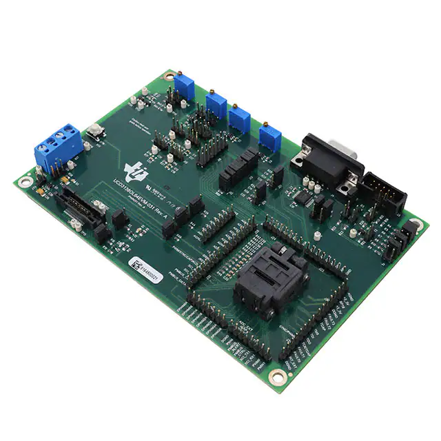
UCD3138OL64CEVM-031 EVM offers an easy to use test platform for stand-alone evaluation of Texas
Instruments’ UCD3138 highly integrated digital controller that is optimized for isolated power applications.
Featuring a 64-pin socket and comprehensive set of test points, the EVM allows hardware and firmware
engineers to manipulate signals on the different pins of the device individually and study open loop
operation. The EVM also offers the flexibility to realize simple closed loop control configurations (using RC
circuits to filter PWM output signals and regulate a DC voltage in closed loop control). Hardware ports
available to communicate with the device include PMBus, UART and JTAG. The EVM accepts up to 5-V
DC input and an on-board 3.3-V LDO can be used to bias the device. Alternately, using jumpers, the
device can be biased using the PMBus communication pins.
NOTE: In order to download firmware and program the UCD3138 device in UCD3138OL64EVM031, a separate EVM from Texas Instruments known as the USB-TO-GPIO Adapter is
required. The USB-TO-GPIO Adapter is NOT supplied with UCD3138OL64EVM-031 and
must be purchased separately. The USB-TO-GPIO Adapter serves as a communication
interface adaptor or a bridge between a host PC and the UCD3138 via a standard type-A to
mini-B USB cable. The USB-TO-GPIO Adapter is listed below in the related products
section.
2
Description
UCD3138OL64EVM-031 is an EVM board, to facilitate evaluation on UCD3138RGC digital power
controller. This EVM provides hardware needed to evaluate UCD3138 64-pin device. All pins of
UCD3138RGC are accessible through header connections, including all GPIO pins, ADC12 pins, front end
pins, DPWM pins, and Fault pins, etc. Particularly, the board has terminal of PMBus, UART DB-9 RS232,
and JTAG. All headers can be jumped to configure for a particular interested evaluation need.
2.1
Typical Applications
•
•
•
2.2
Features
•
•
•
•
•
•
•
•
2
UCD3138RGC Function Evaluation
Firmware Debug
Hardware Design Assistance
Drop-In Socket to Flexible Change the Device
External 5.0-V Supply or PMBus Bias Supply
JTAG Connector
UART Connector, DB-9, RS232
LED Indicators
PMBus Connector to PC Computer Connection Through USB-to-GPIO Adapter
Rich Test Points to Facilitate the Device Evaluation, System Design and Circuit and Firmware
Debugging
Board with Jumpers to Make Flexible Configuration to Adapt Various Evaluation Target
Using the UCD3138OL64EVM-031
SLUUA10 – October 2012
Submit Documentation Feedback
Copyright © 2012, Texas Instruments Incorporated
�Specifications
www.ti.com
3
Specifications
Table 1. UCD3138OL64EVM-031 Specifications
PARAMETER
CONDITIONS
MIN
TYP
MAX
UNITS
Connector J1
JTAG
Standard JTAG communication connection
Standard
Port of connection to USB-to-GPIO, pin definition refer
to TI standard USB-to-GPIO document SLLU093
Standard
Female DB-9, RS232
Standard
Standard JTAG communication connection
Standard
Connector J3
PMBus connector
Connector J4
UART
Connector J5
JTAG
Connector J38
J38-4
Port to use 3.3 V on board to bias external circuit
3.25
3.30
3.45
J38-3
External 5.0 V to board
4.90
5.00
5.10
J38-2
External 3.3 V to board
3.27
3.30
3.33
J38-1
Digital ground DGND
VDC
Operation Environment
Operating temperature range
Natural convection
25
Width
4.0
Length
6.0
Component height
0.5
°C
Mechanical Characteristics
Dimensions
inches
Firmware for Testing
Filename
PWR031_Test_GPIO_ADC12.x0
SLUUA10 – October 2012
Submit Documentation Feedback
Using the UCD3138OL64EVM-031
Copyright © 2012, Texas Instruments Incorporated
3
�[2,5,6]PMBUS_DATA
[2,5,6]PMBUS_CLK
[2,4,5] SCI_TX0
[2,4,5] SCI_RX0
[2,5]PWM0/SYNC/TCAP/ADC_EXT
[1,2,5] /RESET
DGND
16
15
14
13
12
11
10
9
8
[2,3] AD03
[1,2,4,5,6,9]+3_3V
7
6
[2,3] AD04
[2,3] AD06
5
4
[2,3] AD10
[2,3] AD07
2
3
[2,3] AD12
R54
[2,3] AD13
65
AD11 [2,3]
0
[2,5,7] DPWM0A
1
0
XU1
R50
64
AD08 [2,3]
17
AD09 [2,3]
63
18
0
[2,5,7] DPWM0B
R51
62
AD05 [2,3]
61
R55
19
R52
[2,5,7] DPWM1A
0
[2,5,7] DPWM1B
0
20
AD01 [2,3]
60
AD02 [2,3]
59
R56
21
V33A [1,2,4,8]
22
R53
[2,5,7] DPWM2B
0
[2,5,7] DPWM2A
55
26
AD00 [2,3]
57
58
23
0
[2,5,7] DPWM3A
56
25
[2,5] PWM0/ADC_EXT/TCAP/SYNC
24
R57
0
[2,5,7] DPWM3B
54
27
EAP2 [2,3]
53
28
[2,5,6]PMBUS_ALERT
52
29
EAP1 [2,3]
51
30
EAP0 [2,3]
50
31
[2,5] SCI_TX1
Copyright © 2012, Texas Instruments Incorporated
[2,5,6] PMBUS_CTRL
Using the UCD3138OL64EVM-031
[2,5] SCI_RX1
49
32
4
[2,4,5] PWM1
33
34
35
36
37
38
39
40
41
42
43
44
INT_EXT [2,5]
FAULT0 [2,5]
FAULT1 [2,5]
TCK/TCAP/SYNC/PWM0[2,5]
TDO [2,5]
TDI [2,5]
TMS [2,5]
TCAP [2]
FAULT2 [2,5]
FAULT3 [2,5]
BP18 [1,2]
+3_3V [1,2,4,5,6,9]
45
+3_3V[1,2,4,5,6,9]
46
47
48
AGND
C53
1.0uF
DGND
0.1uF
C48
Reset
AGND
DGND
C49
0.1uF
C50
0.1uF
1000pF
C44
+3_3V [1,2,4,5,6,9]
1.0uF
C43
V33A [1,2,4,8]
Local Decoupling
S1
20k
R59
+3_3V
C45
1000pF
C52
1.0uF
1000pF
C46
C51
1.0uF
BP18 [1,2]
+3_3V [1,2,4,5,6,9]
DGND
DGND
1.0uF
C47
/RESET [1,2,5]
4
[2,4,5] PWM0
UCD3138 64 Pin Socket
Schematics
www.ti.com
Schematics
Figure 1. UCD3138OL64EVM-031 Schematics (Socket) 1 of 9
SLUUA10 – October 2012
Submit Documentation Feedback
�8
1
2
3
[1,3] AD03
[1,2,4,5,6,9]+3_3V
[1,2,4,5,6,7] DGND
[1,5] /RESET
[1,5,6] PMBUS_DATA
8
7
6
PMBUS_CLK
[1,4,5] SCI_TX0
[1,5,6]
5
[1,4,5] SCI_RX0
4
6
7
[1,3] AD06
[1,3] AD04
[1,5] PWM0/SYNC/TCAP/ADC_EXT
4
5
[1,3] AD10
[1,3] AD07
3
[1,3] AD12
AD11 [1,3]
J30
J26
AD09 [1,3]
1
1
[1,5,7] DPWM0A
2
AD08 [1,3]
3
[1,5,7] DPWM1A
2
[1,5,7] DPWM0B
3
AD05 [1,3]
AD02 [1,3]
4
4
[1,5,7] DPWM1B
5
J36
AD01 [1,3]
6
6
[1,5,7] DPWM2B
5
[1,5,7] DPWM2A
AD00 [1,3]
V33A [1,4,8]
7
[1,5,7] DPWM3A
7
AGND [1,2,3,4,8,9]
8
[1,2,4,5,6,7] DPWM3B
8
AGND [1,2,3,4,8,9]
1
1
[1,5,7] DGND
2
2
EAP2 [1,3]
3
AGND [1,2,3,4,8,9]
J37
J25
4
4
[1,5,6] PMBUS_CTRL
3
[1,5] PWM0/ADC_EXT/TCAP/SYNC
[1,5,6] PMBUS_ALERT
5
5
AGND [1,2,3,4,8,9]
J31
J27
8
8
EAP1 [1,3]
AGND [1,2,3,4,8,9]
6
6
[1,5] SCI_TX1
7
5
DGND [1,2,4,5,6,7]
TDO [1,5]
8
[1,5]
TDI
2
3
FAULT0 [1,2,5]
INT_EXT [1,5]
TMS [1,5]
1
6
TCAP [1]
8
TCK/TCAP/SYNC/PWM0[1,5]
FAULT1 [1,2,5]
FAULT2 [1,2,5]
4
FAULT3 [1,5]
6
+3_3V [1,2,4,5,6,9]
4
7
BP18 [1]
3
DGND [1,2,4,5,6,7]
+3_3V [1,2,4,5,6,9]
5
AGND [1,2,3,4,8,9]
1
2
[1,2,5] FAULT0
[1,2,5] FAULT1
[1,2,5] FAULT2
DGND
1
3
2
R49
10K
J28
Ground Strip
J32
J40
1
EAP0 [1,3]
7
7
[1,5] SCI_RX1
Copyright © 2012, Texas Instruments Incorporated
[1,4,5] PWM0
SLUUA10 – October 2012
Submit Documentation Feedback
[1,4,5] PWM1
2
J24
3
1
4
2
5
[1,3] AD13
6
[1,2,3,4,8,9]AGND
1
3
2
7
+3_3V
R39
10K
TP17
8
Fault Test Jumpers
1
3
2
AGND
R44
10K
J29
www.ti.com
Schematics
Figure 2. UCD3138OL64EVM-031 Schematics (Headers) 2 of 9
Using the UCD3138OL64EVM-031
5
�Schematics
www.ti.com
ADC12 Filters
R32
100
EADC Filters
R40
100
R43
100
AD02 [1,2]
R38
1k
AD10 [1,2]
AD06 [1,2]
[8] AD02S
[8] AD06S
C23
[8] AD03S
R34
100
R33
100
AD05 [1,2]
AD12 [1,2]
[8] AD12S
C27
100pF
AD13 [1,2]
[8] AD13S
1000pF
1000pF
C32
1000pF
AGND
AGND
AD00 [1,2]
EAP2 [1,2]
AGND
R42
100
AD09 [1,2]
C24
Filter or Address Resistor
EAP2S
C34
AGND
C26
AGND
R36
1k
1000pF
[8] AD09S
[8] AD05S
Filter or Address Resistor
R25
100
AD01 [1,2]
R24
100
3
3
2
C16
[8] AD00S
TP7
R45
100
AGND
R35
C28
AGND
1000pF
AGND
EAP1 [1,2]
100pF
AGND
C25
1000pF
[8] EAP1S
C31
1000pF
AD08 [1,2]
[8] AD08S
C39
100
[8] AD11S
AGND
AD04 [1,2]
R37
1k
AD11 [1,2]
1000pF
AGND
[8] AD04S
AGND
100
C37
1000pF
R48
100
AGND
AD07 [1,2]
[8] AD07S
C35
100pF
R41
R47
100
C29
1000pF
AGND
AD03 [1,2]
[8] EAP0S
C30
1000pF
AGND
R46
100
[8] AD10S
C33
1000pF
EAP0 [1,2]
J21
[8] AD01S
1000pF
1000pF
R29
44.2k
J20
1
1
AGND
2
C14
AGND
C15
1000pF
R28
C13
22.6k
1000pF
AGND
AGND
Figure 3. UCD3138OL64EVM-031 Schematics (Filters) 3 of 9
6
Using the UCD3138OL64EVM-031
SLUUA10 – October 2012
Submit Documentation Feedback
Copyright © 2012, Texas Instruments Incorporated
�C36
10uF
C38
1.0uF
J39
DGND
EN
USB_V33 [6]
+3_3V [1,2,4,5,6,9]
J34
1
3.3V
1
2
FB
OUT
2
DGND
10uF
C41
+
TP13
Jump cross J39, Open J38 - use USB to supply +3.3V
Jump cross J34 (2-3), Open J33 and J39 - use external +3.3V
Jump cross J33, and Jump cross J34 (1-2), Open J34 and J39 - use ext +5V to supply +3.3V
+
GND
IN
U5
TPS76333DBV
+3_3V [1,2,4,5,6,9]
3
2
4
+3.3V OUT
1
3
Ext +5V IN
J33
J38
DGND
(GND1)
TP4
1
GND
+5V_EXT
2
Ext +3.3V IN
Power & LEDs
1
1
AGND
(GND2)
Parts not used
SH1
TieNet
TP16
J2
3
1
2
3
1
2
R2
4.7K
SLUUA10 – October 2012
Submit Documentation Feedback
Copyright © 2012, Texas Instruments Incorporated
DGND
R58
200
PWM0 [1,2,5]
Q1
+
R18
4.7K
DGND
10uF
C42
10K
R3
DGND
MMBT3904TT1G
Q2
D2
LTST-C190CKT
100
R11
AGND
C40
1.0uF
V33A [1,2,8]
+3_3V [1,2,4,5,6,9]
+3_3V [1,2,4,5,6,9]
R66
10
DGND
TP10
R19
10K
MMBT3904TT1G
PWM1 [1,2,5]
D5
LTST-C190YKT
+3_3V
[1,2,4,5,6,9]
J5
SCI_TX0 [1,2,5]
SCI_RX0 [1,2,5]
D1
LTST-C190YKT
R1
100
+3_3V [1,2,4,5,6,9]
www.ti.com
Schematics
Figure 4. UCD3138OL64EVM-031 Schematics (Bias and LEDs) 4 of 9
Using the UCD3138OL64EVM-031
7
�8
JTAG Connector
Using the UCD3138OL64EVM-031
Copyright © 2012, Texas Instruments Incorporated
R6
0
+3_3V
[1,2,4,5,6,9]
TCK/TCAP/SYNC/PWM0
[1,2]
[1,2] TDO
[1,2] TDI
[1,2] TMS
37
35
33
31
29
27
25
23
21
19
17
15
13
11
9
7
10K
R4
DGND
10K
10K
R9
R10
R5 R7
10K 10K
DGND
38
36
34
R8
10K
1
2
3
4
5
6
7
8
9
10
11
12
13
14
DPWM3B [1,2,7]
DPWM3A [1,2,7]
DPWM2B [1,2,7]
DPWM1B [1,2,7]
DPWM2A [1,2,7]
30
DPWM1A [1,2,7]
DPWM0B [1,2,7]
DPWM0A [1,2,7]
J1
PMBUS_DATA [1,2,6]
PMBUS_ALERT [1,2,6]
PMBUS_CTRL [1,2,6]
PMBUS_CLK [1,2,6]
SCI_TX1 [1,2,5]
SCI_RX1 [1,2,5]
32
28
26
24
22
20
18
16
14
12
INT_EXT [1,2]
8
10
6
5
TP14
TP15
[1,2]
PWM0/ADC_EXT/TCAP/SYNC
2
4
1
3
+3_3V
[1,2,4,5,6,9]
TP11
+3_3V
[1,2,4,5,6,9]
[1,2] /RESET
[1,2] PWM0/SYNC/TCAP/ADC_EXT
[1,2,4,5] SCI_RX0
[1,2,4,5]SCI_TX0
[1,2,4] PWM0
[1,2,4] PWM1
[1,2] FAULT3
[1,2] FAULT0
[1,2] FAULT1
[1,2] FAULT2
Logic Analyzer Connector
J35
39
40
41
42
43
TP12
C9
0.1uF
C5
0.1uF
C7
0.1uF
DGND
C10
0.1uF
UART PC Connection
5 C2+
R1OUT 9
T1IN 11
INVALID 10
SCI_RX1
[1,2,5]
SCI_RX0
[1,2,4,5]
SCI_TX1
[1,2,5]
SCI_TX0
[1,2,4,5]
8 R1IN
7 V-
6 C2-
FORCEON 12
GND 14
T1OUT 13
3 V+
4 C1-
VCC 15
FORCEOFF 16
2 C1+
1 EN
U4
SN75C3221DBR
C8
0.1uF
+3_3V
[1,2,4,5,6,9]
1
2
3
1
2
3
TP2 TP1
TP3
11
DGND
10
J17
J16
1
6
2
7
3
8
4
9
5
J4
Schematics
www.ti.com
Figure 5. UCD3138OL64EVM-031 Schematics (UART and JTAG) 5 of 9
SLUUA10 – October 2012
Submit Documentation Feedback
�J3
USB_V33
DGND
1 PMBCTRL5
2 PMBCTRL4
3 PMBCTRL3
4 PMBCTRL2
5 V+
6 GND
7 PMBCTRL1
8 PMBALERT
9 PMBC
10 PMBD
PMBus Interface
J6
33
33
33
33
R20
R12
R13
R14
SLUUA10 – October 2012
Submit Documentation Feedback
Copyright © 2012, Texas Instruments Incorporated
DGND
D3
D4
PMBUS_DATA [1,2,5,6]
PMBUS_CLK [1,2,5,6]
PMBUS_ALERT[1,2,5,6]
PMBUS_CTRL[1,2,5]
PMBUS_ALERT
[1,2,5,6]
PMBUS_DATA
[1,2,5,6]
PMBUS_CLK
[1,2,5,6]
J42
J10
J9
PMBus Pull Up Jumpers
1.5K
R62
1.5K
R23
1.5K
R22
+3_3V
[1,2,4,5,9]
www.ti.com
Schematics
Figure 6. UCD3138OL64EVM-031 Schematics (PMBus) 6 of 9
Using the UCD3138OL64EVM-031
9
�Schematics
www.ti.com
DPWM Filters
TP8
DPWM0A
[1,2,5]
3
J22
R30
2k
2
FLTR-DPWM0
[8]
1
DPWM0B
[1,2,5]
C21
C19
1.0uF
1000pF
DGND
TP9
DPWM1A
[1,2,5]
3
J23
R31
2k
2
FLTR-DPWM1
[8]
1
DPWM1B
C22
C20
1000pF
1
[1,2,5]
DGND
1
Parts not used
TP5
DPWM2A
[1,2,5]
3
J14
R26
2k
2
FLTR-DPWM2
[8]
1
DPWM2B
[1,2,5]
C17
C11
1000pF
1000pF
DGND
TP6
DPWM3A
[1,2,5]
3
J15
R27
2k
2
FLTR-DPWM3
[8]
1
DPWM3B
[1,2,5]
C18
1000pF
C12
1000pF
DGND
Figure 7. UCD3138OL64EVM-031 Schematics (DPWM) 7 of 9
10
Using the UCD3138OL64EVM-031
SLUUA10 – October 2012
Submit Documentation Feedback
Copyright © 2012, Texas Instruments Incorporated
�Schematics
www.ti.com
EADC & ADC12 Feedback
FLTR-DPWM0
FLTR-DPWM1
FLTR-DPWM2
FLTR-DPWM3
V33A
[1,2,4,8]
5
1
2
3
4
5
6
7
8
V+
C3
0.1uF
J11
3
EAP0S
U3
OPA376AIDBV
[3]
J7
1
OUT
4
2
Voltage loop feedback
V-
[7]
[7]
[7]
[7]
EAP1S
R15
20k
[3]
AGND
Current loop feedback
R21
10K
J8
AGND
R60
10K
V33A
J13
V33A
[1,2,4,8]
5
R17
20k
3
1
2
3
4
5
6
7
8
9
10
11
12
13
14
C2
0.1uF
U2
OPA376AIDBV
1
4
C4
2
0.1uF
AGND
AGND
AGND
AD00S [3]
AD02S [3]
AD04S [3]
AD06S [3]
AD08S [3]
AD10S [3]
AD12S [3]
J18
V33A
V33A
[1,2,4,8]
5
R16
20k
J12
3
C6
0.1uF
U1
OPA376AIDBV
1
C1
4
0.1uF
AGND
2
AGND
1
2
3
4
5
6
7
8
9
10
11
12
13
14
AD01S [3]
AD03S [3]
AD05S [3]
AD07S [3]
AD09S [3]
AD11S [3]
AD13S [3]
AGND
Figure 8. UCD3138OL64EVM-031 Schematics (EADC and ADC12) 8 of 9
SLUUA10 – October 2012
Submit Documentation Feedback
Using the UCD3138OL64EVM-031
Copyright © 2012, Texas Instruments Incorporated
11
�Schematics
Primary side voltage sensing test circuit
10K
R64
R63
10K
2
TP19
AGND
1
J41
1
2
AGND
AGND
2N7002
C54
0.1uF
2N7002
Q4
TP22
Ramp generator
TP20
Q3
R65
10K
+3_3V
TP21
20k
R61
+3_3V
Feed forward test circuit
3
J19
TP18
www.ti.com
Figure 9. UCD3138OL64EVM-031 Schematics (Misc) 9 of 9
12
Using the UCD3138OL64EVM-031
SLUUA10 – October 2012
Submit Documentation Feedback
Copyright © 2012, Texas Instruments Incorporated
�Test Equipment
www.ti.com
5
Test Equipment
5.1
PC Computer
5.1.1
Operating System
Microsoft Windows XP (32-bit), or Vista (32-bit), or Windows 7 (32-bit).
5.2
USB-to-GPIO Interface Adapter
This adapter is to establish the communication between the control card UCC3138OL64EVM-031 and the
PC computer through the PMBus and the GUI, Texas Instruments Fusion Digital Power Designer.
5.2.1
USB-to-GPIO Interface Adapter (HPA172)
Accessories including:
• USB interface adapter (HPA172).
• USB cable, 5-pin B mini male to type A male.
• Ribbon cable, socket-to-socket, 10-pin, 2 headers, polarized.
Figure 10. USB-to-GPIO Interface Adapter (HPA172)
5.3
Oscilloscope
An oscilloscope of analog or digital type is capable of 200-MHz bandwidth with Tektronix P6138 or
equivalent oscilloscope probe.
SLUUA10 – October 2012
Submit Documentation Feedback
Using the UCD3138OL64EVM-031
Copyright © 2012, Texas Instruments Incorporated
13
�Equipment Setup
www.ti.com
6
Equipment Setup
6.1
GUI (Graphical User Interface)
6.1.1
File for Installation
The GUI installation file is TI-Fusion-Digital-Power-Designer-Version-1.8.92.exe or newer version. To
get a latest version of GUI, go on TI web site, www.ti.com, search TI Fusion Digital Power Designer
then download and install to one’s computer.
6.1.2
Installation
Double click and launch the .exe file to start the installation. Click Next all the way through. When present,
click I accept the agreement”after read it. Then click install. After the installation, click Finish to exit
setup. Then click Exit Program.
6.1.3
Launch UCD3138 Device GUI
The GUI for UCD3138CC64EVM-030 board can be launched through the below steps:
Click the window start → click All Programs → click Texas Instruments Fusion Digital Power
Designer → click Device GUIs → click UCD3xxx Device GUI.
Figure 11. Device GUI Launch Path
14
Using the UCD3138OL64EVM-031
SLUUA10 – October 2012
Submit Documentation Feedback
Copyright © 2012, Texas Instruments Incorporated
�Equipment Setup
www.ti.com
6.2
6.2.1
Hardware Setup
Setup Overview
Shown below in Figure 12 is the connection between UCD3138OL64EVM-031 and the PC computer
through USB-to-GPIO Interface Adapter.
USB Adapter Connection
• Connect one end of the ribbon cable to the EVM, and connect the other end to the USB interface
adapter
• Connect the Mini connector of the USB cable to the USB interface adapter, and connect the other end
to the USB port of the PC computer.
Figure 12. UCD3138OL64EVM-031 Test Connections
SLUUA10 – October 2012
Submit Documentation Feedback
Using the UCD3138OL64EVM-031
Copyright © 2012, Texas Instruments Incorporated
15
�Equipment Setup
www.ti.com
Figure 13. UCD31xx Device GUI
16
Using the UCD3138OL64EVM-031
SLUUA10 – October 2012
Submit Documentation Feedback
Copyright © 2012, Texas Instruments Incorporated
�Equipment Setup
www.ti.com
Figure 14. Firmware Code Downloading
SLUUA10 – October 2012
Submit Documentation Feedback
Using the UCD3138OL64EVM-031
Copyright © 2012, Texas Instruments Incorporated
17
�Equipment Setup
6.3
www.ti.com
List of Test Points
Table 2. UCD3138OL64EVM-031 Test Point Functions
TEST POINTS
NAME
TP1
UART J4-2
UART transmitting
TP2
UART J4-3
UART receiving
TP3
UART GND
DGND
TP4
J38-1
DGND
TP5
FLTR-DPWM2
TP6
DGND
Digital GND
TP7
EAP2S
EAP2 before filter
TP8
FLTR-DPWM0
DPWM0 front end connection
DPWM1 front end connection
DPWM2 front end connection
TP9
FLTR-DPWM1
TP10
+3.3V
3.3 V
TP11
J35-3
Logic analyzer pin 3
TP12
J35-1
Logic analyzer pin 1
TP13
J38-4
3.3 V to outside circuit
TP14
J35-4
Logic analyzer pin 4
TP15
J35-2
Logic analyzer pin 2
TP16
AGND
AGND
TP17
DGND
DGND
TP18
FFCS
Feed forward control selection
TP19
FFC_adj
Feed forward control adjustment
TP20
Q3 Gate
Ramp generator
TP21
Q3 and Q4 drain
Ramp generator
TP22
Q4 gate
Ramp generator
J1
J2, 5
J3, 6,9,10,42
JTAG
LED D1 and D2 control
PMBus
J4,16,17
UART, DB-9 female, RS232
J7, 8,11
EADC and DPWM
J12,13,18,20,21
ADC12
J14,15, 22, 23
DPWM
J19,41
J24,25,26,27,30,31,36,3
7
J28,29,32
J33,34,38,39
18
DESCRIPTION
Feed forward control
UCD3138 pinout headers
Faults connections
Board bias power management
J35
Logic Analyzer Connector, not populated
J40
AGND strip
S1
UCD3138 reset, press to reset.
Using the UCD3138OL64EVM-031
SLUUA10 – October 2012
Submit Documentation Feedback
Copyright © 2012, Texas Instruments Incorporated
�Test Procedure
www.ti.com
7
Test Procedure
7.1
Download Firmware Codes to UCD3138OL64EVM-031
Set up the EVM connection based on Figure 12.
1. Set up the EVM connection based on Figure 12. The LED of USB adapter is lighted up.
2. Use provided jumper jump across J39. The LED of the EVM is lighted on.
3. Launch the UCD31xx device GUI following the steps described in Section 6.2.1. A window shown in
Figure 13 appears.
4. Check Download program flash, Download data flash and DO NOT write program checksum as
shown in Figure 14.
5. Click Firmware Download; then a new window appears as shown in Figure 14. Click Select File and
browse an intended firmware code file with file extension .x0; then click Download. Click Close to exit
the download window.
6. After the firmware codes downloaded to the UCD3138 device, the intended test can be performed. In
this user’s guide, we use PWR031_Test_GPIO_ADC12.x0 to show how to use the board.
7.2
Example Test and Steps
1. Setup hyper terminal using RS232 serial port with the settings shown. Then launch the hyper terminal.
Figure 15. Hyper Terminal Settings
2. Place jumpers on the following headers, jump across J1 pin-11 and pin-13, i.e., J1(11 and 13), J2(2
and 3), J5(1 and 2), J18(1 and 2, 3 and 4, 5 and 6, 7 and 8, 9 and 10, 11 and 12, 13 and 14), J28(1
and 2), J29(1 and 2), J32(1 and 2).
3. Connect J36 all pins together using single-in-line connector; then use a click-wire, hook-wire connect
J36-1 and J30-4.
4. Place jumpers on J12(1 and 2), J16(1 and 2), J17(1 and 2), J20(2 and 3), J21(2 and 3).
SLUUA10 – October 2012
Submit Documentation Feedback
Using the UCD3138OL64EVM-031
Copyright © 2012, Texas Instruments Incorporated
19
�Test Procedure
www.ti.com
5. Adjust R17 to make ADC12 input to 250 mV by a voltmeter to monitor the voltage between terminal
J13-1 and J40-1.
Figure 16. Location of Jumpers in Use
20
Using the UCD3138OL64EVM-031
SLUUA10 – October 2012
Submit Documentation Feedback
Copyright © 2012, Texas Instruments Incorporated
�Test Procedure
www.ti.com
6. Press Reset button once on the board. Click Command ROM to execute its program
(sendByte0xF0 to Address 11). The firmware downloaded is executed, and the executed result is
transmitted to the hyper terminal as shown.
Figure 17. Execution Result of Example Test
7.3
Equipment Shutdown
1. Exit the GUI and UART.
2. Disconnect the cables.
SLUUA10 – October 2012
Submit Documentation Feedback
Using the UCD3138OL64EVM-031
Copyright © 2012, Texas Instruments Incorporated
21
�EVM Assembly Drawing and PCB layout
8
www.ti.com
EVM Assembly Drawing and PCB layout
The following figures (Figure 18 through Figure 23) show the design of the UCD3138OL64EVM-031
printed circuit board. PCB dimensions: L x W = 6.0 x 4/0 in, PCB material: FR4 or compatible, four layers
and 1-ounce copper on each layer.
Figure 18. UCD3138OL64EVM-031 Top Layer Assembly Drawing (top view)
Figure 19. UCD3138OL64EVM-031 Bottom Assembly Drawing (bottom view)
22
Using the UCD3138OL64EVM-031
SLUUA10 – October 2012
Submit Documentation Feedback
Copyright © 2012, Texas Instruments Incorporated
�EVM Assembly Drawing and PCB layout
www.ti.com
Figure 20. UCD3138OL64EVM-031Top Copper (top view)
Figure 21. UCD3138OL64EVM-031 Internal Layer 1 (top view)
SLUUA10 – October 2012
Submit Documentation Feedback
Using the UCD3138OL64EVM-031
Copyright © 2012, Texas Instruments Incorporated
23
�EVM Assembly Drawing and PCB layout
www.ti.com
Figure 22. UCD3138OL64EVM-031 Internal Layer 2 (top view)
Figure 23. UCD3138OL64EVM-031 Bottom Copper (top view)
24
Using the UCD3138OL64EVM-031
SLUUA10 – October 2012
Submit Documentation Feedback
Copyright © 2012, Texas Instruments Incorporated
�List of Materials
www.ti.com
9
List of Materials
The EVM components list according to the schematics shown in Figure 1 to Figure 9
Table 3. UCD3138OL64EVM-031 List of Materials
QTY
REF DES
DESCRIPTION
PART NUMBER
MFR
14
C1, C2, C3, C4, C5,
C6, C7, C8, C9,
Capacitor, ceramic, 16 V, X7R, 10%, 0.1 µF, 0603
C10, C48, C49, C50,
C54
STD
STD
20
C11,
C17,
C23,
C30,
C34,
STD
STD
5
C13, C15, C44, C45,
Capacitor, ceramic, 50 V, C0G, 5%, 1000 pF, 0603
C46
STD
STD
0
C20
Capacitor, ceramic, 50 V, X7R, 10%, no population,
open, 0603
STD
STD
8
C21, C38, C40, C43,
Capacitor, ceramic, 16 V, X7R, 10%, 1.0 µF, 0603
C47, C51, C52, C53
STD
STD
3
C27, C28, C29
Capacitor, ceramic, 50 V, C0G, 5%, 100 pF, 0603
STD
STD
3
C36, C41, C42
Capacitor, tantalum, 10 V, 20%, 10 µF, 3216
293D106X0010A2T
Vishay
2
D1, D5
Diode, LED, yellow, 2.1 V, 20 mA, 6 mcd, LTSTC190YKT, 0603
LTST-C190YKT
Lite On
1
D2
Diode, LED, red, 2.1 V, 20 mA, 6 mcd, LTST-C190CKT,
LTST-C190CKT
0603
Lite On
2
D3, D4
Diode, dual, Zener, 5.1 V, 300 mW, AZ23C5V1, SOT23 AZ23C5V1-7-F
Diodes
3
J1 ,J13, J18
Header, 2 x 7 pin, 100-mil spacing, 0.100 inch x 2 inch
x 7 inch
PEC07DAAN
Sullins
1
J11
Header, male 2 x 4 pin, 100-mil spacing, 0.20 inch x
0.40 inch
PEC04DAAN
Sullins
15
J2, J5, J14, J15,
J19, J20, J21, J22,
J23,J16, J17, J28,
J29, J32, J34
Header, 3 pin, 100-mil spacing, 0.100 inch x 3 inch
PEC03SAAN
Sullins
9
J24, J25, J26, J27,
J30, J31, J36, J37,
J40
Header, male 8 pin, 100-mil spacing, 0.100 inch x 8
inch
PEC08SAAN
Sullins
1
J3
Connector, male straight 2 x 10 pin, 100-mil spacing, 4
wall, 0.338 inch x 0.788 inch
N2510-6002-RB
3M
1
J35
Plug, 40 pin with hold down, 0.272 inch x 1.000 inch
2-5767004-2
Tyco
1
J38
Terminal block, 4 pin, 15 A, 5.1 mm, 0.80 inch x 0.35
inch
ED120/4DS
OST
1
J4
Connector, 9 pin D, right angle, female, 1.213 inch x
0.510 inch
182-009-212-171
Norcomp
10
J6, J7, J8, J9, J10,
J12, J33, J39, J41,
J42
Header, 2 pin, 100-mil spacing, 0.100 inch x 2 inch
PEC02SAAN
Sullins
2
Q1, Q2
Bipolar, NPN, 40 V, 200 mA, 200 mW, SC-75
MMBT3904TT1G
On Semi
2
Q3, Q4
MOSFET, N-channel, 60 V, 115 mA, 1.2 Ω, SOT23
2N7002-7-F
Diodes
2
R1, R11
Resistor, chip, 1/10 W, 1%, 100 Ω, 0805
STD
STD
4
R12, R13, R14, R20
Resistor, chip, 1/16 W, 5%, 33 Ω, 0603
STD
STD
4
R15, R16, R17, R61
Potentiometer, 3/8 cermet, single turn, right angle, 20
kΩ, 0.288 inch x 0.600 inch
3296Y-1-203 LF
Bourns
2
R2, R18
Resistor, chip, 1/10 W, 1%, 4.7 kΩ, 0603
STD
STD
3
R22, R23, R62
Resistor, chip, 1/16 W, 5%, 1.5 kΩ, 0603
STD
STD
C12,
C18,
C24,
C31,
C35,
C14,
C19,
C25,
C32,
C37,
C16,
C22,
C26, Capacitor, ceramic, 50 V, X7R, 10%, 1000 pF, 0603
C33,
C39
SLUUA10 – October 2012
Submit Documentation Feedback
Using the UCD3138OL64EVM-031
Copyright © 2012, Texas Instruments Incorporated
25
�List of Materials
www.ti.com
Table 3. UCD3138OL64EVM-031 List of Materials (continued)
QTY
REF DES
14
R24,
R34,
R42,
R47,
4
R26, R27, R30, R31
1
1
PART NUMBER
MFR
STD
STD
Resistor, chip, 1/10 W, 1%, 2 kΩ, 0603
STD
STD
R28
Resistor, chip, 1/16 W, 5%, 22.6 kΩ, 0603
STD
STD
R29
Resistor, chip, 1/16 W, 5%, 44.2 kΩ, 0603
STD
STD
16
R3, R4, R5, R7, R8,
R9, R10, R19, R21,
Resistor, chip, 1/16 W, 1%, 10 kΩ, 0603
R39, R44, R49, R60,
R63, R64, R65
STD
STD
3
R36, R37, R38
Resistor, chip, 1/16 W, 1%, 1 kΩ, 0603
STD
STD
1
R58
Resistor, chip, 1/16 W, 5%, 200 Ω, 0603
STD
STD
1
R59
Resistor, chip, 1/16 W, 5%, 20 kΩ, 0603
STD
STD
9
R6, R50, R51, R52,
R53, R54, R55, R56, Resistor, chip, 1/16 W, 1%, 0 Ω, 0603
R57
STD
STD
1
R66
Resistor, chip, 1/16 W, 1%, 10 Ω, 0603
STD
STD
1
S1
Switch, SPST, pb momentary, sealed washable, 0.245
inch x 0.251 inch
KT11P2JM34LFS
C&K
3
U1, U2, U3
Precision, Low Noise, Low Quiescent Current Op-Amp,
SOT23-5
OPA376AIDBVT
TI
1
U4
RS-232 Transceivers with Auto Shutdown, SSOP-16
SN75C3221DBR
TI
1
U5
Micro-Power, 100-mA LDO Regulator, SOT23-5
TPS76333DBVT
TI
1
XU1
Socket, 64-pin Clamshell, 0.800 inch x 1.080 inch
64QN50S19090
Plastronics
PCB, FR-4, 0.062", PCB, 6.000 inch x 4.000 inch
PWR031
any
Digital Power Controller, PFC-64
UCD3138RGC
TI
1
1
26
DESCRIPTION
R25, R32, R33,
R35, R40, R41,
Resistor, chip, 1/16 W, 1%, 100 Ω, 0603
R43, R45, R46,
R48
U6
Using the UCD3138OL64EVM-031
SLUUA10 – October 2012
Submit Documentation Feedback
Copyright © 2012, Texas Instruments Incorporated
�www.ti.com
Appendix A Summary of Using Code Composer Studio v3.3
In this appendix, we describe basic steps how to use Code Composer Studio v3.3, or CCS, to compile
firmware for UCD3138. A design flow is described while detailed steps for firmware code creation, and
firmware debugging along with hardware are obviously beyond the scope of this user’s guide and this
appendix.
A.1
Set up Code Composer Studio v3.3 for UCD3138
The recommended version of Code Composer Studio is v3.3. After completing the CCS v3.3 installation,
and when first time open CCS, a window as shown in Figure 24 is prompted to allow users to select the
required configuration. For the UCD3138 device, please select ARM7 SIMULATOR BIG ENDIAN. Click
ADD and then Save & Quit.
If CCS has existing configurations in My System, click Launch Setup under File pull-down menu. Select
Remove All to remove the existing configurations; then select ARM7 SIMULATOR BIG ENDIAN as
shown in Figure 24, Click ADD and then Save & Quit for UCD3138 device.
Figure 24. Set up Code Composer Studio v3.3 for UCD3138
SLUUA10 – October 2012
Submit Documentation Feedback
Summary of Using Code Composer Studio v3.3
Copyright © 2012, Texas Instruments Incorporated
27
�Build and Compile a Project using Code Composer Studio
A.2
www.ti.com
Build and Compile a Project using Code Composer Studio
After a project is created with all source codes developed, one can compile the project using CCS. On the
matter how to create a project, please refer to reference 2, Code Composer Studio Development Tools
v3.3 – Getting Started Guide. The example below is to describe typical compile process for UCD3138
firmware. The project file name is Cyclone.pjt in a folder named Training 02. The final result is a file with
extension .x0. As the project name is Cyclone.pjt, the final file name Cyclone.x0 is naturally chosen.
Cyclone.x0 is the final firmware code to be downloaded to the UCD3138 device memory for UCD3138
intended functional operation. Here are the steps for a typical compile process.
1. Copy file folder Training 02 in any desired directory inside your PC.
2. Launch CCS and open the CCS project file Cyclone.pjt from the directory where Training 02 was
saved. The following window appears shown in Figure 25.
3. As project Cyclone.pjt has been created and orientated for UCD3138 functions, CCS can be launched
without connecting an emulator.
4. From CCS project window, Right click on Cyclone.pjt (Debug) and then select Build Options… the
window as shown in Figure 26 appears when the Linker tab is selected.
5. Figure 26 shows the project Build Options have been selected to create the file Cyclone.out from
CCS.
6. The next step is to convert file Cyclone.out to Cyclone.x0. “yclone.x0 is the final firmware code to be
downloaded to the UCD3138 device memories. To convert Cyclone.out to Cyclone.x0, the first step
is to click General tab under Build Options for Cyclone.pjt (Debug), as Figure 27 shown, under the
Build Command, confirm the file to be converted is Cyclone.out, then click ok to close Build
Options.
7. Steps 4, 5, and 6 are only necessary once per project. If using a TI developed firmware as a platform,
these steps have been set up and no need to repeat.
8. As shown in Figure 28, select Project M Rebuild All. This generates the file Cyclone.x0 based on
Cyclone.out, and the file of Cyclone.x0 is saved inside the folder where Cyclone.pjt is saved.
Figure 25. Open a Project File Cyclone.pjt (initial open)
28
Summary of Using Code Composer Studio v3.3
Copyright © 2012, Texas Instruments Incorporated
SLUUA10 – October 2012
Submit Documentation Feedback
�Build and Compile a Project using Code Composer Studio
www.ti.com
Figure 26. Open a Project File Cyclone.pjt (build options and linker tab)
Figure 27. Open a Project File Cyclone.pjt (build options and general tab)
SLUUA10 – October 2012
Submit Documentation Feedback
Summary of Using Code Composer Studio v3.3
Copyright © 2012, Texas Instruments Incorporated
29
�References
www.ti.com
Figure 28. Open a Project File Cyclone.pjt (rebuild all)
A.3
References
1. UCD3138 Datasheet, Highly Integrated Digital Controller for Isolated Power, (Texas Instruments
Literature Number SLUSAP2), 2012
2. UCD3138CC64EVM-030 Evaluation Module and User’s Guide, Programmable Digital Power Controller
Control Card Evaluation Module, (Texas Instruments Literature Number SLUU886), 2012
3. TI Application Manual, UCD3138 Digital Power Peripherals Programmer’s Manual, (Texas Instruments
Literature Number SLUU995)
4. TI Application Manual, UCD3138 Monitoring and Communications Programmer’s Manual, (Texas
Instruments Literature Number SLUU996)
5. TI Application Manual, UCD3138 ARM and Digital System Programmer’s Manual, (Texas Instruments
Literature Number SLUU994)
6. User Guide, UCD3138 Isolated Power Fusion GUI, (please contact TI)
30
Summary of Using Code Composer Studio v3.3
Copyright © 2012, Texas Instruments Incorporated
SLUUA10 – October 2012
Submit Documentation Feedback
�EVALUATION BOARD/KIT/MODULE (EVM) ADDITIONAL TERMS
Texas Instruments (TI) provides the enclosed Evaluation Board/Kit/Module (EVM) under the following conditions:
The user assumes all responsibility and liability for proper and safe handling of the goods. Further, the user indemnifies TI from all claims
arising from the handling or use of the goods.
Should this evaluation board/kit not meet the specifications indicated in the User’s Guide, the board/kit may be returned within 30 days from
the date of delivery for a full refund. THE FOREGOING LIMITED WARRANTY IS THE EXCLUSIVE WARRANTY MADE BY SELLER TO
BUYER AND IS IN LIEU OF ALL OTHER WARRANTIES, EXPRESSED, IMPLIED, OR STATUTORY, INCLUDING ANY WARRANTY OF
MERCHANTABILITY OR FITNESS FOR ANY PARTICULAR PURPOSE. EXCEPT TO THE EXTENT OF THE INDEMNITY SET FORTH
ABOVE, NEITHER PARTY SHALL BE LIABLE TO THE OTHER FOR ANY INDIRECT, SPECIAL, INCIDENTAL, OR CONSEQUENTIAL
DAMAGES.
Please read the User's Guide and, specifically, the Warnings and Restrictions notice in the User's Guide prior to handling the product. This
notice contains important safety information about temperatures and voltages. For additional information on TI's environmental and/or safety
programs, please visit www.ti.com/esh or contact TI.
No license is granted under any patent right or other intellectual property right of TI covering or relating to any machine, process, or
combination in which such TI products or services might be or are used. TI currently deals with a variety of customers for products, and
therefore our arrangement with the user is not exclusive. TI assumes no liability for applications assistance, customer product design,
software performance, or infringement of patents or services described herein.
REGULATORY COMPLIANCE INFORMATION
As noted in the EVM User’s Guide and/or EVM itself, this EVM and/or accompanying hardware may or may not be subject to the Federal
Communications Commission (FCC) and Industry Canada (IC) rules.
For EVMs not subject to the above rules, this evaluation board/kit/module is intended for use for ENGINEERING DEVELOPMENT,
DEMONSTRATION OR EVALUATION PURPOSES ONLY and is not considered by TI to be a finished end product fit for general consumer
use. It generates, uses, and can radiate radio frequency energy and has not been tested for compliance with the limits of computing
devices pursuant to part 15 of FCC or ICES-003 rules, which are designed to provide reasonable protection against radio frequency
interference. Operation of the equipment may cause interference with radio communications, in which case the user at his own expense will
be required to take whatever measures may be required to correct this interference.
General Statement for EVMs including a radio
User Power/Frequency Use Obligations: This radio is intended for development/professional use only in legally allocated frequency and
power limits. Any use of radio frequencies and/or power availability of this EVM and its development application(s) must comply with local
laws governing radio spectrum allocation and power limits for this evaluation module. It is the user’s sole responsibility to only operate this
radio in legally acceptable frequency space and within legally mandated power limitations. Any exceptions to this are strictly prohibited and
unauthorized by Texas Instruments unless user has obtained appropriate experimental/development licenses from local regulatory
authorities, which is responsibility of user including its acceptable authorization.
For EVMs annotated as FCC – FEDERAL COMMUNICATIONS COMMISSION Part 15 Compliant
Caution
This device complies with part 15 of the FCC Rules. Operation is subject to the following two conditions: (1) This device may not cause
harmful interference, and (2) this device must accept any interference received, including interference that may cause undesired operation.
Changes or modifications not expressly approved by the party responsible for compliance could void the user's authority to operate the
equipment.
FCC Interference Statement for Class A EVM devices
This equipment has been tested and found to comply with the limits for a Class A digital device, pursuant to part 15 of the FCC Rules.
These limits are designed to provide reasonable protection against harmful interference when the equipment is operated in a commercial
environment. This equipment generates, uses, and can radiate radio frequency energy and, if not installed and used in accordance with the
instruction manual, may cause harmful interference to radio communications. Operation of this equipment in a residential area is likely to
cause harmful interference in which case the user will be required to correct the interference at his own expense.
�FCC Interference Statement for Class B EVM devices
This equipment has been tested and found to comply with the limits for a Class B digital device, pursuant to part 15 of the FCC Rules.
These limits are designed to provide reasonable protection against harmful interference in a residential installation. This equipment
generates, uses and can radiate radio frequency energy and, if not installed and used in accordance with the instructions, may cause
harmful interference to radio communications. However, there is no guarantee that interference will not occur in a particular installation. If
this equipment does cause harmful interference to radio or television reception, which can be determined by turning the equipment off and
on, the user is encouraged to try to correct the interference by one or more of the following measures:
• Reorient or relocate the receiving antenna.
• Increase the separation between the equipment and receiver.
• Connect the equipment into an outlet on a circuit different from that to which the receiver is connected.
• Consult the dealer or an experienced radio/TV technician for help.
For EVMs annotated as IC – INDUSTRY CANADA Compliant
This Class A or B digital apparatus complies with Canadian ICES-003.
Changes or modifications not expressly approved by the party responsible for compliance could void the user’s authority to operate the
equipment.
Concerning EVMs including radio transmitters
This device complies with Industry Canada licence-exempt RSS standard(s). Operation is subject to the following two conditions: (1) this
device may not cause interference, and (2) this device must accept any interference, including interference that may cause undesired
operation of the device.
Concerning EVMs including detachable antennas
Under Industry Canada regulations, this radio transmitter may only operate using an antenna of a type and maximum (or lesser) gain
approved for the transmitter by Industry Canada. To reduce potential radio interference to other users, the antenna type and its gain should
be so chosen that the equivalent isotropically radiated power (e.i.r.p.) is not more than that necessary for successful communication.
This radio transmitter has been approved by Industry Canada to operate with the antenna types listed in the user guide with the maximum
permissible gain and required antenna impedance for each antenna type indicated. Antenna types not included in this list, having a gain
greater than the maximum gain indicated for that type, are strictly prohibited for use with this device.
Cet appareil numérique de la classe A ou B est conforme à la norme NMB-003 du Canada.
Les changements ou les modifications pas expressément approuvés par la partie responsable de la conformité ont pu vider l’autorité de
l'utilisateur pour actionner l'équipement.
Concernant les EVMs avec appareils radio
Le présent appareil est conforme aux CNR d'Industrie Canada applicables aux appareils radio exempts de licence. L'exploitation est
autorisée aux deux conditions suivantes : (1) l'appareil ne doit pas produire de brouillage, et (2) l'utilisateur de l'appareil doit accepter tout
brouillage radioélectrique subi, même si le brouillage est susceptible d'en compromettre le fonctionnement.
Concernant les EVMs avec antennes détachables
Conformément à la réglementation d'Industrie Canada, le présent émetteur radio peut fonctionner avec une antenne d'un type et d'un gain
maximal (ou inférieur) approuvé pour l'émetteur par Industrie Canada. Dans le but de réduire les risques de brouillage radioélectrique à
l'intention des autres utilisateurs, il faut choisir le type d'antenne et son gain de sorte que la puissance isotrope rayonnée équivalente
(p.i.r.e.) ne dépasse pas l'intensité nécessaire à l'établissement d'une communication satisfaisante.
Le présent émetteur radio a été approuvé par Industrie Canada pour fonctionner avec les types d'antenne énumérés dans le manuel
d’usage et ayant un gain admissible maximal et l'impédance requise pour chaque type d'antenne. Les types d'antenne non inclus dans
cette liste, ou dont le gain est supérieur au gain maximal indiqué, sont strictement interdits pour l'exploitation de l'émetteur.
SPACER
SPACER
SPACER
SPACER
SPACER
SPACER
SPACER
SPACER
�【Important Notice for Users of this Product in Japan】
】
This development kit is NOT certified as Confirming to Technical Regulations of Radio Law of Japan
If you use this product in Japan, you are required by Radio Law of Japan to follow the instructions below with respect to this product:
1.
2.
3.
Use this product in a shielded room or any other test facility as defined in the notification #173 issued by Ministry of Internal Affairs and
Communications on March 28, 2006, based on Sub-section 1.1 of Article 6 of the Ministry’s Rule for Enforcement of Radio Law of
Japan,
Use this product only after you obtained the license of Test Radio Station as provided in Radio Law of Japan with respect to this
product, or
Use of this product only after you obtained the Technical Regulations Conformity Certification as provided in Radio Law of Japan with
respect to this product. Also, please do not transfer this product, unless you give the same notice above to the transferee. Please note
that if you could not follow the instructions above, you will be subject to penalties of Radio Law of Japan.
Texas Instruments Japan Limited
(address) 24-1, Nishi-Shinjuku 6 chome, Shinjuku-ku, Tokyo, Japan
http://www.tij.co.jp
【ご使用にあたっての注】
本開発キットは技術基準適合証明を受けておりません。
本製品のご使用に際しては、電波法遵守のため、以下のいずれかの措置を取っていただく必要がありますのでご注意ください。
1.
2.
3.
電波法施行規則第6条第1項第1号に基づく平成18年3月28日総務省告示第173号で定められた電波暗室等の試験設備でご使用いただく。
実験局の免許を取得後ご使用いただく。
技術基準適合証明を取得後ご使用いただく。
なお、本製品は、上記の「ご使用にあたっての注意」を譲渡先、移転先に通知しない限り、譲渡、移転できないものとします。
上記を遵守頂けない場合は、電波法の罰則が適用される可能性があることをご留意ください。
日本テキサス・インスツルメンツ株式会社
東京都新宿区西新宿6丁目24番1号
西新宿三井ビル
http://www.tij.co.jp
SPACER
SPACER
SPACER
SPACER
SPACER
SPACER
SPACER
SPACER
SPACER
SPACER
SPACER
SPACER
SPACER
SPACER
SPACER
SPACER
�EVALUATION BOARD/KIT/MODULE (EVM)
WARNINGS, RESTRICTIONS AND DISCLAIMERS
For Feasibility Evaluation Only, in Laboratory/Development Environments. Unless otherwise indicated, this EVM is not a finished
electrical equipment and not intended for consumer use. It is intended solely for use for preliminary feasibility evaluation in
laboratory/development environments by technically qualified electronics experts who are familiar with the dangers and application risks
associated with handling electrical mechanical components, systems and subsystems. It should not be used as all or part of a finished end
product.
Your Sole Responsibility and Risk. You acknowledge, represent and agree that:
1.
2.
3.
4.
You have unique knowledge concerning Federal, State and local regulatory requirements (including but not limited to Food and Drug
Administration regulations, if applicable) which relate to your products and which relate to your use (and/or that of your employees,
affiliates, contractors or designees) of the EVM for evaluation, testing and other purposes.
You have full and exclusive responsibility to assure the safety and compliance of your products with all such laws and other applicable
regulatory requirements, and also to assure the safety of any activities to be conducted by you and/or your employees, affiliates,
contractors or designees, using the EVM. Further, you are responsible to assure that any interfaces (electronic and/or mechanical)
between the EVM and any human body are designed with suitable isolation and means to safely limit accessible leakage currents to
minimize the risk of electrical shock hazard.
You will employ reasonable safeguards to ensure that your use of the EVM will not result in any property damage, injury or death, even
if the EVM should fail to perform as described or expected.
You will take care of proper disposal and recycling of the EVM’s electronic components and packing materials.
Certain Instructions. It is important to operate this EVM within TI’s recommended specifications and environmental considerations per the
user guidelines. Exceeding the specified EVM ratings (including but not limited to input and output voltage, current, power, and
environmental ranges) may cause property damage, personal injury or death. If there are questions concerning these ratings please contact
a TI field representative prior to connecting interface electronics including input power and intended loads. Any loads applied outside of the
specified output range may result in unintended and/or inaccurate operation and/or possible permanent damage to the EVM and/or
interface electronics. Please consult the EVM User's Guide prior to connecting any load to the EVM output. If there is uncertainty as to the
load specification, please contact a TI field representative. During normal operation, some circuit components may have case temperatures
greater than 60°C as long as the input and output are maintained at a normal ambient operating temperature. These components include
but are not limited to linear regulators, switching transistors, pass transistors, and current sense resistors which can be identified using the
EVM schematic located in the EVM User's Guide. When placing measurement probes near these devices during normal operation, please
be aware that these devices may be very warm to the touch. As with all electronic evaluation tools, only qualified personnel knowledgeable
in electronic measurement and diagnostics normally found in development environments should use these EVMs.
Agreement to Defend, Indemnify and Hold Harmless. You agree to defend, indemnify and hold TI, its licensors and their representatives
harmless from and against any and all claims, damages, losses, expenses, costs and liabilities (collectively, "Claims") arising out of or in
connection with any use of the EVM that is not in accordance with the terms of the agreement. This obligation shall apply whether Claims
arise under law of tort or contract or any other legal theory, and even if the EVM fails to perform as described or expected.
Safety-Critical or Life-Critical Applications. If you intend to evaluate the components for possible use in safety critical applications (such
as life support) where a failure of the TI product would reasonably be expected to cause severe personal injury or death, such as devices
which are classified as FDA Class III or similar classification, then you must specifically notify TI of such intent and enter into a separate
Assurance and Indemnity Agreement.
Mailing Address: Texas Instruments, Post Office Box 655303, Dallas, Texas 75265
Copyright © 2012, Texas Instruments Incorporated
�STANDARD TERMS AND CONDITIONS FOR EVALUATION MODULES
1.
Delivery: TI delivers TI evaluation boards, kits, or modules, including any accompanying demonstration software, components, or
documentation (collectively, an “EVM” or “EVMs”) to the User (“User”) in accordance with the terms and conditions set forth herein.
Acceptance of the EVM is expressly subject to the following terms and conditions.
1.1 EVMs are intended solely for product or software developers for use in a research and development setting to facilitate feasibility
evaluation, experimentation, or scientific analysis of TI semiconductors products. EVMs have no direct function and are not
finished products. EVMs shall not be directly or indirectly assembled as a part or subassembly in any finished product. For
clarification, any software or software tools provided with the EVM (“Software”) shall not be subject to the terms and conditions
set forth herein but rather shall be subject to the applicable terms and conditions that accompany such Software
1.2 EVMs are not intended for consumer or household use. EVMs may not be sold, sublicensed, leased, rented, loaned, assigned,
or otherwise distributed for commercial purposes by Users, in whole or in part, or used in any finished product or production
system.
2
Limited Warranty and Related Remedies/Disclaimers:
2.1 These terms and conditions do not apply to Software. The warranty, if any, for Software is covered in the applicable Software
License Agreement.
2.2 TI warrants that the TI EVM will conform to TI's published specifications for ninety (90) days after the date TI delivers such EVM
to User. Notwithstanding the foregoing, TI shall not be liable for any defects that are caused by neglect, misuse or mistreatment
by an entity other than TI, including improper installation or testing, or for any EVMs that have been altered or modified in any
way by an entity other than TI. Moreover, TI shall not be liable for any defects that result from User's design, specifications or
instructions for such EVMs. Testing and other quality control techniques are used to the extent TI deems necessary or as
mandated by government requirements. TI does not test all parameters of each EVM.
2.3 If any EVM fails to conform to the warranty set forth above, TI's sole liability shall be at its option to repair or replace such EVM,
or credit User's account for such EVM. TI's liability under this warranty shall be limited to EVMs that are returned during the
warranty period to the address designated by TI and that are determined by TI not to conform to such warranty. If TI elects to
repair or replace such EVM, TI shall have a reasonable time to repair such EVM or provide replacements. Repaired EVMs shall
be warranted for the remainder of the original warranty period. Replaced EVMs shall be warranted for a new full ninety (90) day
warranty period.
3
Regulatory Notices:
3.1 United States
3.1.1
Notice applicable to EVMs not FCC-Approved:
This kit is designed to allow product developers to evaluate electronic components, circuitry, or software associated with the kit
to determine whether to incorporate such items in a finished product and software developers to write software applications for
use with the end product. This kit is not a finished product and when assembled may not be resold or otherwise marketed unless
all required FCC equipment authorizations are first obtained. Operation is subject to the condition that this product not cause
harmful interference to licensed radio stations and that this product accept harmful interference. Unless the assembled kit is
designed to operate under part 15, part 18 or part 95 of this chapter, the operator of the kit must operate under the authority of
an FCC license holder or must secure an experimental authorization under part 5 of this chapter.
3.1.2
For EVMs annotated as FCC – FEDERAL COMMUNICATIONS COMMISSION Part 15 Compliant:
CAUTION
This device complies with part 15 of the FCC Rules. Operation is subject to the following two conditions: (1) This device may not
cause harmful interference, and (2) this device must accept any interference received, including interference that may cause
undesired operation.
Changes or modifications not expressly approved by the party responsible for compliance could void the user's authority to
operate the equipment.
FCC Interference Statement for Class A EVM devices
NOTE: This equipment has been tested and found to comply with the limits for a Class A digital device, pursuant to part 15 of
the FCC Rules. These limits are designed to provide reasonable protection against harmful interference when the equipment is
operated in a commercial environment. This equipment generates, uses, and can radiate radio frequency energy and, if not
installed and used in accordance with the instruction manual, may cause harmful interference to radio communications.
Operation of this equipment in a residential area is likely to cause harmful interference in which case the user will be required to
correct the interference at his own expense.
SPACER
SPACER
SPACER
SPACER
SPACER
SPACER
SPACER
SPACER
�FCC Interference Statement for Class B EVM devices
NOTE: This equipment has been tested and found to comply with the limits for a Class B digital device, pursuant to part 15 of
the FCC Rules. These limits are designed to provide reasonable protection against harmful interference in a residential
installation. This equipment generates, uses and can radiate radio frequency energy and, if not installed and used in accordance
with the instructions, may cause harmful interference to radio communications. However, there is no guarantee that interference
will not occur in a particular installation. If this equipment does cause harmful interference to radio or television reception, which
can be determined by turning the equipment off and on, the user is encouraged to try to correct the interference by one or more
of the following measures:
•
•
•
•
Reorient or relocate the receiving antenna.
Increase the separation between the equipment and receiver.
Connect the equipment into an outlet on a circuit different from that to which the receiver is connected.
Consult the dealer or an experienced radio/TV technician for help.
3.2 Canada
3.2.1
For EVMs issued with an Industry Canada Certificate of Conformance to RSS-210
Concerning EVMs Including Radio Transmitters:
This device complies with Industry Canada license-exempt RSS standard(s). Operation is subject to the following two conditions:
(1) this device may not cause interference, and (2) this device must accept any interference, including interference that may
cause undesired operation of the device.
Concernant les EVMs avec appareils radio:
Le présent appareil est conforme aux CNR d'Industrie Canada applicables aux appareils radio exempts de licence. L'exploitation
est autorisée aux deux conditions suivantes: (1) l'appareil ne doit pas produire de brouillage, et (2) l'utilisateur de l'appareil doit
accepter tout brouillage radioélectrique subi, même si le brouillage est susceptible d'en compromettre le fonctionnement.
Concerning EVMs Including Detachable Antennas:
Under Industry Canada regulations, this radio transmitter may only operate using an antenna of a type and maximum (or lesser)
gain approved for the transmitter by Industry Canada. To reduce potential radio interference to other users, the antenna type
and its gain should be so chosen that the equivalent isotropically radiated power (e.i.r.p.) is not more than that necessary for
successful communication. This radio transmitter has been approved by Industry Canada to operate with the antenna types
listed in the user guide with the maximum permissible gain and required antenna impedance for each antenna type indicated.
Antenna types not included in this list, having a gain greater than the maximum gain indicated for that type, are strictly prohibited
for use with this device.
Concernant les EVMs avec antennes détachables
Conformément à la réglementation d'Industrie Canada, le présent émetteur radio peut fonctionner avec une antenne d'un type et
d'un gain maximal (ou inférieur) approuvé pour l'émetteur par Industrie Canada. Dans le but de réduire les risques de brouillage
radioélectrique à l'intention des autres utilisateurs, il faut choisir le type d'antenne et son gain de sorte que la puissance isotrope
rayonnée équivalente (p.i.r.e.) ne dépasse pas l'intensité nécessaire à l'établissement d'une communication satisfaisante. Le
présent émetteur radio a été approuvé par Industrie Canada pour fonctionner avec les types d'antenne énumérés dans le
manuel d’usage et ayant un gain admissible maximal et l'impédance requise pour chaque type d'antenne. Les types d'antenne
non inclus dans cette liste, ou dont le gain est supérieur au gain maximal indiqué, sont strictement interdits pour l'exploitation de
l'émetteur
3.3 Japan
3.3.1
Notice for EVMs delivered in Japan: Please see http://www.tij.co.jp/lsds/ti_ja/general/eStore/notice_01.page 日本国内に
輸入される評価用キット、ボードについては、次のところをご覧ください。
http://www.tij.co.jp/lsds/ti_ja/general/eStore/notice_01.page
3.3.2
Notice for Users of EVMs Considered “Radio Frequency Products” in Japan: EVMs entering Japan may not be certified
by TI as conforming to Technical Regulations of Radio Law of Japan.
If User uses EVMs in Japan, not certified to Technical Regulations of Radio Law of Japan, User is required by Radio Law of
Japan to follow the instructions below with respect to EVMs:
1.
2.
3.
Use EVMs in a shielded room or any other test facility as defined in the notification #173 issued by Ministry of Internal
Affairs and Communications on March 28, 2006, based on Sub-section 1.1 of Article 6 of the Ministry’s Rule for
Enforcement of Radio Law of Japan,
Use EVMs only after User obtains the license of Test Radio Station as provided in Radio Law of Japan with respect to
EVMs, or
Use of EVMs only after User obtains the Technical Regulations Conformity Certification as provided in Radio Law of Japan
with respect to EVMs. Also, do not transfer EVMs, unless User gives the same notice above to the transferee. Please note
that if User does not follow the instructions above, User will be subject to penalties of Radio Law of Japan.
SPACER
SPACER
SPACER
SPACER
SPACER
�【無線電波を送信する製品の開発キットをお使いになる際の注意事項】 開発キットの中には技術基準適合証明を受けて
いないものがあります。 技術適合証明を受けていないもののご使用に際しては、電波法遵守のため、以下のいずれかの
措置を取っていただく必要がありますのでご注意ください。
1.
2.
3.
電波法施行規則第6条第1項第1号に基づく平成18年3月28日総務省告示第173号で定められた電波暗室等の試験設備でご使用
いただく。
実験局の免許を取得後ご使用いただく。
技術基準適合証明を取得後ご使用いただく。
なお、本製品は、上記の「ご使用にあたっての注意」を譲渡先、移転先に通知しない限り、譲渡、移転できないものとします。
上記を遵守頂けない場合は、電波法の罰則が適用される可能性があることをご留意ください。 日本テキサス・イ
ンスツルメンツ株式会社
東京都新宿区西新宿6丁目24番1号
西新宿三井ビル
3.3.3
Notice for EVMs for Power Line Communication: Please see http://www.tij.co.jp/lsds/ti_ja/general/eStore/notice_02.page
電力線搬送波通信についての開発キットをお使いになる際の注意事項については、次のところをご覧くださ
い。http://www.tij.co.jp/lsds/ti_ja/general/eStore/notice_02.page
SPACER
4
EVM Use Restrictions and Warnings:
4.1 EVMS ARE NOT FOR USE IN FUNCTIONAL SAFETY AND/OR SAFETY CRITICAL EVALUATIONS, INCLUDING BUT NOT
LIMITED TO EVALUATIONS OF LIFE SUPPORT APPLICATIONS.
4.2 User must read and apply the user guide and other available documentation provided by TI regarding the EVM prior to handling
or using the EVM, including without limitation any warning or restriction notices. The notices contain important safety information
related to, for example, temperatures and voltages.
4.3 Safety-Related Warnings and Restrictions:
4.3.1
User shall operate the EVM within TI’s recommended specifications and environmental considerations stated in the user
guide, other available documentation provided by TI, and any other applicable requirements and employ reasonable and
customary safeguards. Exceeding the specified performance ratings and specifications (including but not limited to input
and output voltage, current, power, and environmental ranges) for the EVM may cause personal injury or death, or
property damage. If there are questions concerning performance ratings and specifications, User should contact a TI
field representative prior to connecting interface electronics including input power and intended loads. Any loads applied
outside of the specified output range may also result in unintended and/or inaccurate operation and/or possible
permanent damage to the EVM and/or interface electronics. Please consult the EVM user guide prior to connecting any
load to the EVM output. If there is uncertainty as to the load specification, please contact a TI field representative.
During normal operation, even with the inputs and outputs kept within the specified allowable ranges, some circuit
components may have elevated case temperatures. These components include but are not limited to linear regulators,
switching transistors, pass transistors, current sense resistors, and heat sinks, which can be identified using the
information in the associated documentation. When working with the EVM, please be aware that the EVM may become
very warm.
4.3.2
EVMs are intended solely for use by technically qualified, professional electronics experts who are familiar with the
dangers and application risks associated with handling electrical mechanical components, systems, and subsystems.
User assumes all responsibility and liability for proper and safe handling and use of the EVM by User or its employees,
affiliates, contractors or designees. User assumes all responsibility and liability to ensure that any interfaces (electronic
and/or mechanical) between the EVM and any human body are designed with suitable isolation and means to safely
limit accessible leakage currents to minimize the risk of electrical shock hazard. User assumes all responsibility and
liability for any improper or unsafe handling or use of the EVM by User or its employees, affiliates, contractors or
designees.
4.4 User assumes all responsibility and liability to determine whether the EVM is subject to any applicable international, federal,
state, or local laws and regulations related to User’s handling and use of the EVM and, if applicable, User assumes all
responsibility and liability for compliance in all respects with such laws and regulations. User assumes all responsibility and
liability for proper disposal and recycling of the EVM consistent with all applicable international, federal, state, and local
requirements.
5.
Accuracy of Information: To the extent TI provides information on the availability and function of EVMs, TI attempts to be as accurate
as possible. However, TI does not warrant the accuracy of EVM descriptions, EVM availability or other information on its websites as
accurate, complete, reliable, current, or error-free.
SPACER
SPACER
SPACER
SPACER
SPACER
SPACER
�SPACER
6.
Disclaimers:
6.1 EXCEPT AS SET FORTH ABOVE, EVMS AND ANY WRITTEN DESIGN MATERIALS PROVIDED WITH THE EVM (AND THE
DESIGN OF THE EVM ITSELF) ARE PROVIDED "AS IS" AND "WITH ALL FAULTS." TI DISCLAIMS ALL OTHER
WARRANTIES, EXPRESS OR IMPLIED, REGARDING SUCH ITEMS, INCLUDING BUT NOT LIMITED TO ANY IMPLIED
WARRANTIES OF MERCHANTABILITY OR FITNESS FOR A PARTICULAR PURPOSE OR NON-INFRINGEMENT OF ANY
THIRD PARTY PATENTS, COPYRIGHTS, TRADE SECRETS OR OTHER INTELLECTUAL PROPERTY RIGHTS.
6.2 EXCEPT FOR THE LIMITED RIGHT TO USE THE EVM SET FORTH HEREIN, NOTHING IN THESE TERMS AND
CONDITIONS SHALL BE CONSTRUED AS GRANTING OR CONFERRING ANY RIGHTS BY LICENSE, PATENT, OR ANY
OTHER INDUSTRIAL OR INTELLECTUAL PROPERTY RIGHT OF TI, ITS SUPPLIERS/LICENSORS OR ANY OTHER THIRD
PARTY, TO USE THE EVM IN ANY FINISHED END-USER OR READY-TO-USE FINAL PRODUCT, OR FOR ANY
INVENTION, DISCOVERY OR IMPROVEMENT MADE, CONCEIVED OR ACQUIRED PRIOR TO OR AFTER DELIVERY OF
THE EVM.
7.
USER'S INDEMNITY OBLIGATIONS AND REPRESENTATIONS. USER WILL DEFEND, INDEMNIFY AND HOLD TI, ITS
LICENSORS AND THEIR REPRESENTATIVES HARMLESS FROM AND AGAINST ANY AND ALL CLAIMS, DAMAGES, LOSSES,
EXPENSES, COSTS AND LIABILITIES (COLLECTIVELY, "CLAIMS") ARISING OUT OF OR IN CONNECTION WITH ANY
HANDLING OR USE OF THE EVM THAT IS NOT IN ACCORDANCE WITH THESE TERMS AND CONDITIONS. THIS OBLIGATION
SHALL APPLY WHETHER CLAIMS ARISE UNDER STATUTE, REGULATION, OR THE LAW OF TORT, CONTRACT OR ANY
OTHER LEGAL THEORY, AND EVEN IF THE EVM FAILS TO PERFORM AS DESCRIBED OR EXPECTED.
8.
Limitations on Damages and Liability:
8.1 General Limitations. IN NO EVENT SHALL TI BE LIABLE FOR ANY SPECIAL, COLLATERAL, INDIRECT, PUNITIVE,
INCIDENTAL, CONSEQUENTIAL, OR EXEMPLARY DAMAGES IN CONNECTION WITH OR ARISING OUT OF THESE
TERMS ANDCONDITIONS OR THE USE OF THE EVMS PROVIDED HEREUNDER, REGARDLESS OF WHETHER TI HAS
BEEN ADVISED OF THE POSSIBILITY OF SUCH DAMAGES. EXCLUDED DAMAGES INCLUDE, BUT ARE NOT LIMITED
TO, COST OF REMOVAL OR REINSTALLATION, ANCILLARY COSTS TO THE PROCUREMENT OF SUBSTITUTE GOODS
OR SERVICES, RETESTING, OUTSIDE COMPUTER TIME, LABOR COSTS, LOSS OF GOODWILL, LOSS OF PROFITS,
LOSS OF SAVINGS, LOSS OF USE, LOSS OF DATA, OR BUSINESS INTERRUPTION. NO CLAIM, SUIT OR ACTION SHALL
BE BROUGHT AGAINST TI MORE THAN ONE YEAR AFTER THE RELATED CAUSE OF ACTION HAS OCCURRED.
8.2 Specific Limitations. IN NO EVENT SHALL TI'S AGGREGATE LIABILITY FROM ANY WARRANTY OR OTHER OBLIGATION
ARISING OUT OF OR IN CONNECTION WITH THESE TERMS AND CONDITIONS, OR ANY USE OF ANY TI EVM
PROVIDED HEREUNDER, EXCEED THE TOTAL AMOUNT PAID TO TI FOR THE PARTICULAR UNITS SOLD UNDER
THESE TERMS AND CONDITIONS WITH RESPECT TO WHICH LOSSES OR DAMAGES ARE CLAIMED. THE EXISTENCE
OF MORE THAN ONE CLAIM AGAINST THE PARTICULAR UNITS SOLD TO USER UNDER THESE TERMS AND
CONDITIONS SHALL NOT ENLARGE OR EXTEND THIS LIMIT.
9.
Return Policy. Except as otherwise provided, TI does not offer any refunds, returns, or exchanges. Furthermore, no return of EVM(s)
will be accepted if the package has been opened and no return of the EVM(s) will be accepted if they are damaged or otherwise not in
a resalable condition. If User feels it has been incorrectly charged for the EVM(s) it ordered or that delivery violates the applicable
order, User should contact TI. All refunds will be made in full within thirty (30) working days from the return of the components(s),
excluding any postage or packaging costs.
10. Governing Law: These terms and conditions shall be governed by and interpreted in accordance with the laws of the State of Texas,
without reference to conflict-of-laws principles. User agrees that non-exclusive jurisdiction for any dispute arising out of or relating to
these terms and conditions lies within courts located in the State of Texas and consents to venue in Dallas County, Texas.
Notwithstanding the foregoing, any judgment may be enforced in any United States or foreign court, and TI may seek injunctive relief
in any United States or foreign court.
Mailing Address: Texas Instruments, Post Office Box 655303, Dallas, Texas 75265
Copyright © 2015, Texas Instruments Incorporated
spacer
�IMPORTANT NOTICE
Texas Instruments Incorporated and its subsidiaries (TI) reserve the right to make corrections, enhancements, improvements and other
changes to its semiconductor products and services per JESD46, latest issue, and to discontinue any product or service per JESD48, latest
issue. Buyers should obtain the latest relevant information before placing orders and should verify that such information is current and
complete. All semiconductor products (also referred to herein as “components”) are sold subject to TI’s terms and conditions of sale
supplied at the time of order acknowledgment.
TI warrants performance of its components to the specifications applicable at the time of sale, in accordance with the warranty in TI’s terms
and conditions of sale of semiconductor products. Testing and other quality control techniques are used to the extent TI deems necessary
to support this warranty. Except where mandated by applicable law, testing of all parameters of each component is not necessarily
performed.
TI assumes no liability for applications assistance or the design of Buyers’ products. Buyers are responsible for their products and
applications using TI components. To minimize the risks associated with Buyers’ products and applications, Buyers should provide
adequate design and operating safeguards.
TI does not warrant or represent that any license, either express or implied, is granted under any patent right, copyright, mask work right, or
other intellectual property right relating to any combination, machine, or process in which TI components or services are used. Information
published by TI regarding third-party products or services does not constitute a license to use such products or services or a warranty or
endorsement thereof. Use of such information may require a license from a third party under the patents or other intellectual property of the
third party, or a license from TI under the patents or other intellectual property of TI.
Reproduction of significant portions of TI information in TI data books or data sheets is permissible only if reproduction is without alteration
and is accompanied by all associated warranties, conditions, limitations, and notices. TI is not responsible or liable for such altered
documentation. Information of third parties may be subject to additional restrictions.
Resale of TI components or services with statements different from or beyond the parameters stated by TI for that component or service
voids all express and any implied warranties for the associated TI component or service and is an unfair and deceptive business practice.
TI is not responsible or liable for any such statements.
Buyer acknowledges and agrees that it is solely responsible for compliance with all legal, regulatory and safety-related requirements
concerning its products, and any use of TI components in its applications, notwithstanding any applications-related information or support
that may be provided by TI. Buyer represents and agrees that it has all the necessary expertise to create and implement safeguards which
anticipate dangerous consequences of failures, monitor failures and their consequences, lessen the likelihood of failures that might cause
harm and take appropriate remedial actions. Buyer will fully indemnify TI and its representatives against any damages arising out of the use
of any TI components in safety-critical applications.
In some cases, TI components may be promoted specifically to facilitate safety-related applications. With such components, TI’s goal is to
help enable customers to design and create their own end-product solutions that meet applicable functional safety standards and
requirements. Nonetheless, such components are subject to these terms.
No TI components are authorized for use in FDA Class III (or similar life-critical medical equipment) unless authorized officers of the parties
have executed a special agreement specifically governing such use.
Only those TI components which TI has specifically designated as military grade or “enhanced plastic” are designed and intended for use in
military/aerospace applications or environments. Buyer acknowledges and agrees that any military or aerospace use of TI components
which have not been so designated is solely at the Buyer's risk, and that Buyer is solely responsible for compliance with all legal and
regulatory requirements in connection with such use.
TI has specifically designated certain components as meeting ISO/TS16949 requirements, mainly for automotive use. In any case of use of
non-designated products, TI will not be responsible for any failure to meet ISO/TS16949.
Products
Applications
Audio
www.ti.com/audio
Automotive and Transportation
www.ti.com/automotive
Amplifiers
amplifier.ti.com
Communications and Telecom
www.ti.com/communications
Data Converters
dataconverter.ti.com
Computers and Peripherals
www.ti.com/computers
DLP® Products
www.dlp.com
Consumer Electronics
www.ti.com/consumer-apps
DSP
dsp.ti.com
Energy and Lighting
www.ti.com/energy
Clocks and Timers
www.ti.com/clocks
Industrial
www.ti.com/industrial
Interface
interface.ti.com
Medical
www.ti.com/medical
Logic
logic.ti.com
Security
www.ti.com/security
Power Mgmt
power.ti.com
Space, Avionics and Defense
www.ti.com/space-avionics-defense
Microcontrollers
microcontroller.ti.com
Video and Imaging
www.ti.com/video
RFID
www.ti-rfid.com
OMAP Applications Processors
www.ti.com/omap
TI E2E Community
e2e.ti.com
Wireless Connectivity
www.ti.com/wirelessconnectivity
Mailing Address: Texas Instruments, Post Office Box 655303, Dallas, Texas 75265
Copyright © 2015, Texas Instruments Incorporated
�