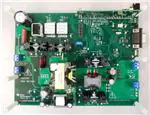
Using the UCD3138PSFBEVM-027
User's Guide
Literature Number: SLUUAK4
August 2013
�www.ti.com
WARNING
Always follow TI’s set-up and application instructions, including use of all interface components within their
recommended electrical rated voltage and power limits. Always use electrical safety precautions to help
ensure your personal safety and the safety of those working around you. Contact TI’s Product Information
Center http://support/ti./com for further information.
Save all warnings and instructions for future reference.
Failure to follow warnings and instructions may result in personal injury, property damage, or
death due to electrical shock and/or burn hazards.
The term TI HV EVM refers to an electronic device typically provided as an open framed, unenclosed
printed circuit board assembly. It is intended strictly for use in development laboratory environments,
solely for qualified professional users having training, expertise, and knowledge of electrical safety risks in
development and application of high-voltage electrical circuits. Any other use and/or application are strictly
prohibited by Texas Instruments. If you are not suitably qualified, you should immediately stop from further
use of the HV EVM.
1. Work Area Safety:
(a) Keep work area clean and orderly.
(b) Qualified observer(s) must be present anytime circuits are energized.
(c) Effective barriers and signage must be present in the area where the TI HV EVM and its interface
electronics are energized, indicating operation of accessible high voltages may be present, for the
purpose of protecting inadvertent access.
(d) All interface circuits, power supplies, evaluation modules, instruments, meters, scopes and other
related apparatus used in a development environment exceeding 50 VRMS/75 VDC must be
electrically located within a protected Emergency Power Off (EPO) protected power strip.
(e) Use a stable and non-conductive work surface.
(f) Use adequately insulated clamps and wires to attach measurement probes and instruments. No
freehand testing whenever possible.
2. Electrical Safety:
(a) De-energize the TI HV EVM and all its inputs, outputs, and electrical loads before performing any
electrical or other diagnostic measurements. Revalidate that TI HV EVM power has been safely deenergized.
(b) With the EVM confirmed de-energized, proceed with required electrical circuit configurations, wiring,
measurement equipment hook-ups and other application needs, while still assuming the EVM circuit
and measuring instruments are electrically live.
(c) Once EVM readiness is complete, energize the EVM as intended.
WARNING: while the EVM is energized, never touch the EVM or its electrical circuits as they
could be at high voltages capable of causing electrical shock hazard.
3. Personal Safety:
(a) Wear personal protective equipment e.g. latex gloves and/or safety glasses with side shields or
protect EVM in an adequate lucent plastic box with interlocks from accidental touch.
4. Limitation for Safe Use:
(a) EVMs are not to be used as all or part of a production unit.
Fusion Digital Power is a trademark of Texas Instruments.
2
SLUUAK4 – August 2013
Submit Documentation Feedback
Copyright © 2013, Texas Instruments Incorporated
�User's Guide
SLUUAK4 – August 2013
Using the UCD3138PSFBEVM-027
1
Introduction
This evaluation model (EVM), the UCD3138PSFBEVM-027, is used to evaluate the UCD3138 64-pin
digital control IC in an off-line power-converter application and then to aid in its design. The EVM is a
standalone phase-shifted full-bridge DC-DC power converter. The EVM is used together with a control
card, the UCD3138CC64EVM-030, which is an EVM placed on the UCD3138RGC.
The UCD3138PSFBEVM-027, together with the UCD3138CC64EVM-030, evaluates a phase-shifted fullbridge DC-DC converter. Each EVM is delivered without requiring additional work, from either hardware or
firmware. This EVM combination allows for some of the design parameters to be retuned using Texas
Instruments' graphical user interface (GUI) based tool, Fusion Digital Power™ Designer. Loading custom
firmware with user-designed definition and development is also possible.
Three EVMs are included in the kit: the UCD3138PSFBEVM-027, UCD3138CC64EVM-030, and USB-TOGPIO.
This user’s guide provides basic evaluation instruction with a focus on system operation in a standalone
phase-shifted full-bridge DC-DC power converter.
WARNING
High voltages are present on this evaluation module during
operation and for a a time period after power off. This module
should only be tested by skilled personnel in a controlled
laboratory environment.
An isolated DC voltage source meeting IEC61010 reinforced
insulation standards is recommended for evaluating this EVM.
High temperature exceeding 60°C may be found during EVM
operation and for a time period after power off.
The purpose of this EVM is to facilitate the evaluation of digital
control in a phase-shifted full-bridge DC-DC converter using the
UCD3138, and cannot be tested and treated as a final product.
Extreme caution should be taken to eliminate the possibility of
electric shock and heat burn. Please refer to the page Evaluation
Module Electrical Safety Guideline after the cover page for your
safety concerns and precautions.
Read and understand this user’s guide thoroughly before starting
any physical evaluation.
SLUUAK4 – August 2013
Submit Documentation Feedback
Using the UCD3138PSFBEVM-027
Copyright © 2013, Texas Instruments Incorporated
3
�Description
2
www.ti.com
Description
The UCD3138PSFBEVM-027, along with the UCD3138CC64EVM-030, demonstrates a phase-shifted fullbridge DC-DC power converter with digital control using the UCD3138 device. The UCD3138 device is
located on the UCD3138CC64EVM-030 board. The UCD3138CC64EVM-030 is a daughter-card with
preloaded firmware providing the required control functions for an phase-shifted full-bridge converter.
Please contact TI for details on the firmware. The UCD3138PSFBEVM-027 accepts a DC input from 370
to 400 VDC, and outputs a typical 12 VDC with full-load output power at 360 W, or full output current of 30
A.
NOTE: This EVM does not have an input fuse. It relies on the input current limit from the input
voltage source that is used.
2.1
Typical Applications
•
•
•
2.2
Features
•
•
•
•
•
•
•
•
4
Offline DC-DC power conversions
Servers
Telecommunication systems
Digitally-controlled phase-shifted full-bridge DC-DC power conversion
DC input from 370 to 400 VDC
12-VDC regulated output from no load to full load
Full-load power at 360 W, or full-load current at 30 A
High efficiency
Constant soft-start time
Overvoltage, overcurrent, and brownout protection
Test points to facilitate device and topology evaluation
Using the UCD3138PSFBEVM-027
SLUUAK4 – August 2013
Submit Documentation Feedback
Copyright © 2013, Texas Instruments Incorporated
�Performance Specifications
www.ti.com
3
Performance Specifications
Table 1. UCD3138PSFBEVM-027 Performance Specifications (1)
PARAMETER
TEST CONDITIONS
MIN
TYP
MAX
UNITS
400
VDC
Input Characteristics
Voltage operation
range
370
Input UVLO On
350
Input UVLO Off
Input current
VDC
330
VDC
Input = 370 VDC, full load = 30 A
1.2
Input = 385 VDC, full load = 30 A
1.1
Input = 400 VDC, full load = 30 A
1
A
Output Characteristics
Output voltage, VOUT No load to full load
Output over voltage
Output load current,
IOUT (1)
370 to 400 VDC
Output voltage ripple
385 VDC and full load = 30 A
Output over current
12
VDC
13.5
VDC
30
90
A
mVpp
30
A
Systems Characteristics
Switching frequency
140
kHz
Peak efficiency
385 VDC, full load = 30 A
93.5
%
Full-load efficiency
385 VDC, load = 30 A
93.5
%
Operating
temperature
400-LFM forced air flow cooling
25
°C
Firmware
Device ID (Version)
UCD3100ISO1 | 0.0.01.0001|130315
Filename
UCD3138PSFBPWR027_03152013.x0
(1)
The load current and load power are commanded using the designer GUI. See Section 12 for more information on CPCC
operation. See Section 13 for more information on GUI application.
SLUUAK4 – August 2013
Submit Documentation Feedback
Using the UCD3138PSFBEVM-027
Copyright © 2013, Texas Instruments Incorporated
5
�Schematics
4
www.ti.com
Schematics
TP1
+VIN
J1
+VIN
Isolation Boundary
Primary
Secondary
BUS+
TP3
C61
J9
L1
2.2µH
Current Doubler Rectifier and Filter
TP19
TP17
Q10
SI7866ADP
C7
+RS
1nF
4700pF
C44
T1
R32
C50
1.5µF
4700pF
11
10
D21
STPS130A
0
D20
R4
R6
2.43
7.50
QSYN1
D10
QT1
R1
5.11k
2
L2
22µH
TP33
R5
R20
15.0k
C60
R21
15.0k
9
STPS130A
2
1 2
QSYN2
R3
5.11k
DPWM3A
C55
0.1µF
TP21
8
7
6
HS1
1 2
D1
TP28
C53
INA
VDD
GND
INB
OUTB
PWPD
TP14
1
R90
10.0k
2
3
R51
1.21k
4
R104
0.003
INA
VDD
GND
R34
DPWM0B
4
R88
10.0k
R35
T3
10
1
9
2
R103
5.11k
DPWM2A
BUS_ITRAN
R23
2.49k
80mH
TP25
R29
R28
150
1
10.0k
R73
TP35
D18
C17
100pF
5
2
1:1:1
D16
C54
TP29
1
2.43
R46
BAT54S
4
3
R72
1
7
6
VAUXS
OUTA
INA
VDD
GND
OUTB
PWPD
INB
2
C18
1µF
AGND
DPWM2A
TP4
TP6
6
VAUXS
5
C25
1µF
ENBA
OUTA
INA
GND
VDD
OUTB
PWPD
INB
OVP_LATCH
2
2
TP5
3
4
1
4
VAUX_S
VAUX_P
VIN_MONITOR
-VAUX_-VIN
RSVD
GND
GATE
100pF
10
9
J2
C10
0.1µF
8
1
+RS
2
VAUXS
1.00
5
GND
R43
VINSCALED
6
R100
1.0k
TP7
R93
1.0k
Auxiliary Bias Supply
1
R91
220
TP23
R87
C12
10nF
1
EAP2
DPWM1A
DPWM_1A
AGND
DPWM1B
DPWM_1B
C67
DPWM2A 3.3V_EXT
DPWM_2A
DPWM_2B
DPWM3A
R77
2.05k
R17
36.5k
R30
R78
0
1.24k
I_PRI
C24
AGND
DPWM3B
DPWM_3B
330pF
C58
0.1µF
DPWM2B
DPWM_3A
C13
4.7µF
1
2
3
4
IN
OUT
NC
NC
NC
NC
GND
FB/NC
PWPD
9
C46
2200pF
AD_02/I_SHARE
DPWM0B
DPWM_0B
1
DPWM0A
3.3V_EXT
U9
TPS715A33
7
-VIN
DPWM3A
DPWM3B
C
UV
11
Q1
VAUXS
VIN+
3
9
7
ENBB
OV
C71
12
DPWM0A
DPWM_0A
TP8
U6
PWR050
1
U5
UCC27424DGN
A
ORING_GATE
1
2
3
4
5
6
7
8
9
10
11
12
13
14
15
16
1 2
+VIN
8
FLTB
13
P3
HS2
DPWM2B
VAUXPRI
FLTR
-RS
3
4
7
BYP
STAT
ORing Control
D17
1
C11
10nF
RSET
C9
0.1uF
14
3
BAV70-V
9
5
ENBA
ENBB
C64
220pF
BAT54S
R10
5.11k
8
R41
100k
R42
10.0k
PG
VDD
QB2
0.1µF
D25
OVP_LATCH
5
GPIO/ORING_CTRL
R71
150
7.50
U4
UCC27424DGN
3
4
D14
DPWM2B
2
TP12
6
J10
R9
1
TP9
D12
T5
1
C8
100pF
U1
TPS2411PW
R40
10.0
R39
10.0k
Primary Current Sense
1
R38
549
VAUXS
C23
220pF
AGND
BAV70-V
6
C6
4700pF
C16
4700pF
+VO1
AD_06
4
QT2
2.43
+VO
C65
0.1µF
R37
R31
1
3
R8
5.11k
0.1µF
R49
1.21k
R50
1.21k
IS-
7.50
C28
J8
15.0
3
3.32k
100
TP16 TP15
R54
IS-
J4
12-V Return
-RS
1nF
2
INB
OUTB
PWPD
1000µF
C4
1000µF
C5
R105
0.003
I_PRI
T2
2
OUTA
+
C3
47µF
C62
+
C63
47µF
C2
47µF
C1
47µF
1
ENBA
ENBB
+VO1
R52
1.21k
1.00
TP24
MMBD914
0.1uF
D27
ENBA
OUTA
R70
BUS+
BAV70-V
D19
5
R66
10.0k
TP34
STPS130A
R36
ENBB
U8
UCC27424DGN
VAUXS
D23
2.43
5
C22
0.1µF
TP22
QSYN4
7.50
R2
6
VAUXS
1.00
R12
51.1
5
1:1:1
6
R26
10.0k
R27
100pF
0.1uF
D8
R7
R24
10.0k
C21
1
0.1µF
C19
QB1
TP27
C56
1.00
10nF
HS3
D9
D24
7
R53
0.003
BAV70-V
100
T4
D7
ORING_GATE
2
TP36
D22
10
8
R25
+12-V Output
30A J3
+VO
DPWM1B
U3
UCC27424DGN
TP20
C20
IS-
1 2
100pF
MBRS1100
C59
DPWM3B
C43
7
HS4
1.00
R48
10.0k
QSYN3
D5
8
6
TP26
C36
0.1µF
400-V Return
R11
51.1
MBRS1100
9
R19
J11
R47
D6
12
1
0
BUS_ITRAN
9
+
C66
47µF
TP2
9
+400-V Input
R55
15.0
Q6
SI7866ADP
Q2
1
TP32
Q8
Q4
1
1
1
8
7
R44
6
1
DPWM1A
R22
0.5
External Slope Compensation
AGND
5
R45
100k
C14
10nF
C15
10µF
Parts not populated
IS-
Figure 1. UCD3138PSFBEVM-027 Schematics, Sheet 1 of 2
6
Using the UCD3138PSFBEVM-027
SLUUAK4 – August 2013
Submit Documentation Feedback
Copyright © 2013, Texas Instruments Incorporated
�Schematics
www.ti.com
+VO1
AD_03
R75
3.32k
SN75C3221
R80
1.82k
C45
1nF
C42
100pF
1
C31
0.1µF
R76
AGND
4
R82
16.2k
R83
1.82k
C47
1nF
U10
LM60C
1
3.3V_EXT
C29
6
0.1µF
7
8
V+
GND
C1-
T1OUT
C2+
FORCEON
T1IN
C2V-
INVALID
R1OUT
R1IN
16
15
C33
1µF
1
6
2
7
3
8
4
9
5
14
13
12
11
10
9
2
GPIO/ACFAIL_IN
AGND
AD_07
GND
C32
0.1µF
3.3V_EXT
3
C37
0.1uF
VCC
Temp = 0.5 + .01*T
VOUT
+VS
5
AD_09
+VO
Current buffer and noise filter
0.1 x Vout
FORCEOFF
C1+
3
EAN1
0
AGND
EN
2
10
2.00k
C38
10nF
C30
0.1µF
SCI_RX1
3.3V_EXT
J7
D13
BAT54S
AGND
SCI_TX1
AD_08
1.00k
Temperature sensor
SCI_RX0
1
2
3
4
5
6
R84
VINSCALED
AGND
AGND
1
2
3
4
5
6
7
8
9
10
11
12
13
14
15
16
17
18
19
20
21
22
23
24
25
26
27
28
29
30
31
32
33
34
35
36
37
38
39
40
J6
U7
16.2k
11
EAP1
P2
3.3V_EXT
R79
0.0343 x Iout
R74
ISEC
C68
10nF
R101
100k
SCI_TX0
Serial UART Interface
C48
1nF
TP41
AGND
AD00
AD_02/I_SHARE
AD_03
AD_04
AD_05
AD_06
AD_07
AD_08
AD_09
AD_13
EAP2
EAN1
EAP1
EAN0
EAP0
AGND
R85
R65
1.00k
10.0k
C49
1nF
C39
10nF
S1
C69
AD_13
ISEC
ON/OFF
3.3V_EXT
R16
R15
C70
CHASSIS
0.1µF
AGND
Noise reducing low pass filtering
R86
+VO
3.3V_EXT
499
C34
3.3V_EXT
R81
499
OVP_LATCH
R92
10.0k
220pF
R102
R18
10.0k
C26
1500pF
IS-
Q7-B
MMDT3946
3.3V_EXT
R69
49.9K
1
Q7-A
MMDT3946
R89
4.99k
EMI Control
AGND
OV threshold at 15.6 V
D15
15V
1
2
3
4
5
6
7
8
9
10
11
12
13
14
15
16
17
18
19
20
21
22
23
24
25
26
27
28
29
30
31
32
33
34
35
36
37
38
39
40
PWM0
1
1
C57
10nF
ON/OFF Manual Switching
and noise conditioning
TP13
P1
0.1µF
R13
10.0
R68
U2
TP37
1.00k
Parts not populated
ISEC
C35
0.1uF
R67
C51
2200pF
1
0.0549 x Iout
OPA345NA
OVP Latch
R14
0
1.00k
DPWM_0A
DPWM_0B
DPWM_1A
DPWM_1B
DPWM_2A
DPWM_2B
DPWM_3A
DPWM_3B
GPIO/ACFAIL_IN
GPIO/ACFAIL_OUT
ON/OFF
GPIO/FAILURE
GPIO/P_GOOD
SCI_TX1
SCI_RX1
PWM0
GPIO/ORING_CTRL
SCI_TX0
SCI_RX0
2
VAUXS
3
3.3V_EXT
AGND
AGND
Ground connection
Current Sense Amplifier (Low Offset/ X66.5)
J5
1
C40
0.1µF
C41
0.1µF
R94
549
R60
301
549
R96
R97
549
16.2k
0.1 x Vout
D11
+VO1
R98
1.82k
D3
LTST-C190GKT
C52
1nF
-RS
EAN0
R58
10.0k
1.62k
C27
100pF
Output voltage divider and noise filter
GPIO/P_GOOD
D2
LTST-C190CKT
R62
3.32k
R56
3.32k
R99
D4
LTST-C190GKT
Q9
MMBT3904LT1G
Q3
MMBT3904LT1G
R59
3.32k
D26
LTST-C190CKT
Q5
MMBT3904LT1G
R61
10.0k
R64
10.0k
GPIO/FAILURE
R33
1.00k
R57
301
301
R63
EAP0
+RS
VAUXPRI
3.3V_EXT
3.3V_EXT
3.3V_EXT
R95
Power On
GPIO/ACFAIL_OUT
LED Status indicators
AGND
Figure 2. UCD3138PSFBEVM-027 Schematics Sheet, 2 of 2
SLUUAK4 – August 2013
Submit Documentation Feedback
Using the UCD3138PSFBEVM-027
Copyright © 2013, Texas Instruments Incorporated
7
�Schematics
www.ti.com
TP1
3.3VD
3.3VA
R39
1
1
1
15
EADC-P0
RESET
EADC-N0
/RESET
C16
33pF
TP23
50
1
51
EADC-P1
TP6
DGND
TP21
TP24
TP22
1
1
1
EADC-P2
TP5
EADC-N2
AD-00
C14
AD-00
AD-01
R15
100K
1000pF
R17
R16
TP34
TP32
1
AD-09
AD-10
AD-11
R21
2K
R20
100
100
1
TP27
1
100
60
TP29
8
7
1
TP28
61
1
TP30
100
R26
R24
TP26
1
100
6
TP31
1
2K
2K
5
62
4
64
3
2K
AD-12
AD-13
R28
R29
R23
1
100
R25
2
2K
2K
TP33 TP35 TP36
1
1
1
65
C19
C18
C21
C20
C23
C22
C25
C24
C27
C26
C29
C28
C30
C31
9
46
47
45
RESET
PMBUS_CLK
U1
TCAP
UCD3138RGC
EAP0
EAN0
TDO
TDI
39
EAP1
DPWM0A
EAN1
DPWM0B
EAP2
TMS
40
/RESET
11
TP12 TP13
DPWM-0A
17
TP14 TP15
DPWM2B
DPWM3A
AD02
AD03
AD04
DPWM3B
AD05
DPWM-1A
TP17 TP18
AD07
TP19
23
DPWM-3A
24
EXT-TRIG
SCI-RX0
SCI-TX0
SYNC
35
FAULT-0
FAULT1
36
FAULT2
42
FAULT-1
FAULT-2
FAULT3
43
FAULT-3
29
SCI-TX1
SCI_RX1 30
SCI-RX1
SCI_TX1
PWPD
DPWM-3B
INT-EXT
SCI_RX0 13
SCI_TX0 14
SYNC
FAULT0
DPWM-2B
TP20
INT_EXT 34
ADC_EXT
AD10
AD11
AD12
AD13
1000pF 1000pF 1000pF 1000pF 1000pF 1000pF 1000pF 1000pF 1000pF 1000pF 1000pF 1000pF 1000pF 1000pF
DPWM-2A
22
26
AD08
AD09
DPWM-1B
21
12
AD06
DPWM-0B
18
20
DPWM2A
TP16
TCAP
41
DPWM1A 19
DPWM1B
EAN2
58
63
R22
R27
1
R19
55
TP25
R18
AD-03
AD-04
AD-05
AD-06
AD-07
AD-08
54
C17
33pF
TMS
AD01
59
AD00
AD-02
DGND
53
100
100
AGND
52
C15
33pF
EADC-N1
C13
0.1µF
PMBUS_ALERT
PMBUS_DATA
TCK
37
TP2
R10
10K
C7
100pF
DGND
10
1
16
DGND
S1
TP9
TCK
TDO 38
TDI
33
R12
1.65K
TP8
DGND
PWM1
DGND
27
TP11
TP10
C8
DGND
100
R9
C12
2.2µF
1000pF
PMBUS_CTRL
44
28
C11
0.1µF
16K
DGND
25
32
PWM0
DGND
31
DGND
3.3VD
TP3
BP18
DGND
PMBUS-CLK
56 AGND
3.3VD
33pF
C9
TP7
PWM-1
D2
BAT54A
V33DIO
33pF
V33D
C10
PWM-0
J2
C6
1µF
R11
V33DIO
TP4
PMBUS-DATA
100
R8
C5
0.1µF
AGND
57
100
R13
1.5K
AGND
R7
C4
0.1µF
DGND
R14
1.5K
PMBUS-ALERT
V33A
D1
BAT54A
48
1
C3
0.1µF
C1
1µF
0.1µF
3.3VD
AGND
1
C2
PMBUS-CTRL
AGND
1
100
0
1
1
1
2
3
4
5
6
7
8
9
10
R5
R6
R4
R3
49
R2
R1
J1
10
NS1
AGND
1
DGND
1
Parts not used
Figure 3. UCD3138CC64EVM-030 Schematics, Sheet 1 of 2
8
Using the UCD3138PSFBEVM-027
SLUUAK4 – August 2013
Submit Documentation Feedback
Copyright © 2013, Texas Instruments Incorporated
�Schematics
www.ti.com
J3
PPPN202FJFN
J4
PPPN202FJFN
1
2
3
4
5
6
7
8
9
10
11
12
13
14
15
16
17
18
19
20
21
22
23
24
25
26
27
28
29
30
31
32
33
34
35
36
37
38
39
40
DPWM-0A
DPWM-0B
DPWM-1A
DPWM-1B
1
2
3
4
5
6
7
8
9
10
11
12
13
14
15
16
17
18
19
20
21
22
23
24
25
26
27
28
29
30
31
32
33
34
35
36
37
38
39
40
AD-00
AD-01
AD-02
AD-03
AD-04
AD-05
AD-06
AD-07
AD-08
AD-09
AD-10
AD-11
AD-12
AD-13
EADC-N2
EADC-P2
EADC-N1
EADC-P1
EADC-N0
EADC-P0
DPWM-2A
DPWM-2B
DPWM-3A
DPWM-3B
FAULT-0
FAULT-1
SYNC
FAULT-2
FAULT-3
SCI-TX1
SCI-RX1
PWM-0
PWM-1
TCAP
SCI-TX0
SCI-RX0
INT-EXT
EXT-TRIG
/RESET
+12V_EXT
DGND
AGND
3.3VD
If needed, use this jumper
to provide 3.3VD to application board
J6
3.3VD
R32
10K
R34
0
R35
10K
J5
TMS
TDI
TDO
TCK
R36
0
3.3VD
R37
10K
R38
10K
1
2
3
4
5
6
7
8
9
10
11
12
13
14
U2
TPS715A33DRBR
3.3VD
D3
R30
0.5
C34
0.1µF
R31
301
8 OUT
IN 1
7 NC
NC 2
6 NC
NC 3
5 FB/NC
9 PWPD
R33
10K
GND 4
TP37
+12V_EXT
C32
1µF
C33
10µF
DGND
DGND
Figure 4. UCD3138CC64EVM-030 Schematics, Sheet 2 of 2
SLUUAK4 – August 2013
Submit Documentation Feedback
Using the UCD3138PSFBEVM-027
Copyright © 2013, Texas Instruments Incorporated
9
�Test Setup
www.ti.com
5
Test Setup
5.1
Test Equipment
DC voltage source: This source is capable of 350 to 400 VDC. The source is adjustable, with a minimum
power rating of 400 W, or current rating no less than 1.5 A, and has a current limit function. The DC
voltage source used should meet IEC61010 safety requirements.
DC multi-meter: The multi-meter has two units, one is capable of a 0 to 400 VDC input range and
preferred four-digit display. The other unit is capable of a 0 to 15 VDC input range and a preferred fourdigit display.
Output load: This DC load is capable of receiving 0 to 15 VDC, 0 to 30 A, and 0 to 360-W or greater, with
display such as load current and load power.
Current meter: If the load does not have a display, this DC current-meter is optional. This unit is capable
of 0 to 30 A. A low-ohmic shunt and DMM are recommended.
Oscilloscope: The oscilloscope is capable of 500-MHz full bandwidth, digital or analog. If choosing a
digital oscilloscope, TI recommends 5 Gs/s or better.
Fan: A fan with 400-LFM forced-air cooling is required.
Recommended wire gauge: The recommended gauge must be capable of 30 A, or better than No. 14
AWG, with the total wire length less than 8 ft (4-ft input and 4-ft return).
5.2
Recommended Test Setup
P2
PWR030
P1
D2
D3
D4
P3
S1
2
4
6
8
10
12
14
16
UART1
1
3
5
7
9
11
13
15
J6
+VIN
-VIN
J1 TP1
TP17
J3
+VOUT
J4
-VOUT
J11
TP2
TP15
D26
PWR050
Figure 5. UCD3138PSFBEVM-027 Recommended Test Setup
10
Using the UCD3138PSFBEVM-027
SLUUAK4 – August 2013
Submit Documentation Feedback
Copyright © 2013, Texas Instruments Incorporated
�Test Points
www.ti.com
Figure 6. Orientation of the UCD3138CC64EVM-030 Board on the UCD3138PSFBEVM-027 Board
6
Test Points
Table 2. UCD3138PSFBEVM-027 List of Test Points
Test Points
Name
TP1
+VIN
Positive input voltage
TP2
–VIN
Input voltage return
TP3
BUS+
Primary high-side current-sense input
TP4
VAUXPRI
Primary 12-V bias
TP5
PWRGND
Primary 12-V bias return
TP6
VAUX_S
TP7
PGND
TP8
VINSCALED
TP9
Ipri
TP10
TP11
Description
Secondary 12-V bias
Secondary 12-V bias return
VIN sense on the secondary side
Primary current sense
Control-card mechanical-guide pin
Not used
TP12
FLTB
Oring control
TP13
PGND
Secondary 12-V bias return
TP14
+VO1
Output before oring FETs
TP15
PGND
Secondary 12-V bias return
TP16
–RS
Remote sense of the output voltage
TP17
VO
Output voltage positive terminal
TP18
Not used
TP19
+RS
TP20
SR1-3
Remote sense of the output voltage
QSYN 1 and 3 drive
TP21
SR2-4
QSYN 2 and 4 drive
TP22
IS–
Load current sense
TP23
AGND
TP24
Ipri
Analog ground
Primary current sense (AD_06)
SLUUAK4 – August 2013
Submit Documentation Feedback
Using the UCD3138PSFBEVM-027
Copyright © 2013, Texas Instruments Incorporated
11
�Terminals
www.ti.com
Table 2. UCD3138PSFBEVM-027 List of Test Points (continued)
7
Test Points
Name
TP25
AGND
Description
Analog ground
TP26
QT1_Gate
QT1 gate
TP27
QB1_Gate
QB1 gate
TP28
QT2_Gate
QT2 gate
TP29
QB2_Gate
QB2 gate
TP30
Not used
TP31
Not used
TP32
3.3V
3.3 V
TP33
SW1
Switch node
TP34
PWRGND
TP35
SW2
Switch Node
TP36
CASS
Primary commutation-assist junction
TP37
ISEC
IOUT sensing output (EADC1 Input)
TP38
Not used
TP39
Not used
TP40
Not used
TP41
S1
Primary 12-V bias return
S1 status
Terminals
Table 3. List of Terminals
12
Terminal
Name
J1
Input_P
Input voltage positive terminal
Description
J2
Remote Sense
Remote sense and I_SHARE
J3
12VO
+12-V output
J4
–12VO
12-V output return
J5
Bias
J6
UART1
Standard UART connection, RS232, 9-pin
J7
UART0
UART0 and ACFAIL_IN (communication with PFC)
J8
VO_RIPPLE
J9
Jumper
Jumper (reserved to an input-fuse substitution)
J10
Jumper
Used when T5 not populated
J11
Input_N
Input voltage return terminal
VAUX_S and 3.3V_EXT
BNC VO_Ripple
Using the UCD3138PSFBEVM-027
SLUUAK4 – August 2013
Submit Documentation Feedback
Copyright © 2013, Texas Instruments Incorporated
�Test Procedure
www.ti.com
8
Test Procedure
8.1
Efficiency Measurement Procedure
WARNING
Danger of electrical
measurement!
shock!
High
voltage
present
during
CAUTION
Do not leave the EVM powered when unattended.
CAUTION
Danger of heat burn from high temperature.
1. See Figure 4 for basic setup to measure power-conversion efficiency. The required equipment for this
measurement is listed in Figure 5.
2. Check the boards visually before making electrical connections to ensure that no shipping damage
occurred.
3. Use the UCD3138PSFBEVM-027 and UCD3138CC64EVM-030 for this measurement which are
included this EVM package along with the USB-TO-GPIO.
4. Install the UCD3138CC64EVM-030 board onto the UCD3138PSFBEVM-027 first. Take care with the
alignment and orientation of the two boards to avoid damage.
• See Figure 6 for the UCD3138PFCEVM-030 board orientation.
5. Connect the DC-voltage source to J1 (+) and J11 (–). The DC-voltage source should be isolated and
meet IEC61010 requirements.
• Set up the DC-output voltage in the range specified in Table 1, between 370 VDC and 400V DC;
set the DC-source current limit at 1.2 A.
NOTE: A fuse is not installed on the board and, therefore, the board relies on the current limit of the
external voltage source for circuit protection.
6. Connect an electronic load with either a constant-current mode or constant-resistance mode. The load
range is from 0 to 30 A.
7. Ensure a jumper is installed on J6 of the UCD3138CC64EVM-030
8. Use the switch S1 to turn on the board output after the input voltage is applied to the board. Before
applying input voltage, ensure that the switch, S1, is in the OFF position.
9. Use a current meter or low-ohmic shunt and DMM between the load and the board for current
measurements if the load does not have a current or a power display.
10. Connect a volt-meter across the output connector and set the volt-meter scale at 0 to 15 V (DC).
11. Turn on the DC-voltage source output. Flip S1 to ON and vary the load.
12. Record output voltage and current measurements.
8.2
Equipment Shutdown Procedure
1. Shut down the DC-voltage source
2. Shut down the electronic load.
SLUUAK4 – August 2013
Submit Documentation Feedback
Using the UCD3138PSFBEVM-027
Copyright © 2013, Texas Instruments Incorporated
13
�Performance Data and Typical Characteristics Curves
9
www.ti.com
Performance Data and Typical Characteristics Curves
Figure 7, Figure 8, Figure 9, Figure 10, Figure 11, Figure 9, Figure 10, Figure 12, Figure 13, Figure 14,
and Figure 15 present typical performance curves for the UCD3138PSFBEVM-027.
9.1
Efficiency
100
95
Efficiency (%)
90
85
80
75
70
370 VDC
385 VDC
400 VDC
65
60
5
10
15
20
25
30
Load Current (A)
C001
Figure 7. UCD3138PSFBEVM-027 Efficiency
9.2
Load Regulation
12.3
Load Regulation (V)
12.1
11.9
11.7
11.5
370 VDC
385 VDC
400 VDC
11.3
5
10
15
20
25
Load Current (A)
30
C002
Figure 8. UCD3138PSFBEVM-027 Load Regulation
14
Using the UCD3138PSFBEVM-027
SLUUAK4 – August 2013
Submit Documentation Feedback
Copyright © 2013, Texas Instruments Incorporated
�Performance Data and Typical Characteristics Curves
www.ti.com
9.3
Switching Waveforms
Figure 9. Gate-Drive Signals at No Load
Figure 10. Gate-Drive Signals at Full Load
Ch1 = QT1 gate to GND (TP26)
Ch3 = QSYN1 Vgs (TP20)
Ch2 = QB2 Vgs (TP29)
Ch4 = QSYN2 Vgs (TP21)
SLUUAK4 – August 2013
Submit Documentation Feedback
Using the UCD3138PSFBEVM-027
Copyright © 2013, Texas Instruments Incorporated
15
�Performance Data and Typical Characteristics Curves
www.ti.com
Figure 11. Primary-Side Switching
Ch1 = QB1 Vgs
Ch3 = QB2 Vgs
9.4
Ch2 = QB1 Vds
Ch4 = QB2 Vds
Output Voltage Ripple
Figure 12. Output Voltage Ripple, 385 VDC and Full Load
16
Using the UCD3138PSFBEVM-027
SLUUAK4 – August 2013
Submit Documentation Feedback
Copyright © 2013, Texas Instruments Incorporated
�Performance Data and Typical Characteristics Curves
www.ti.com
Figure 13. Output Voltage Ripple, 385 VDC and Half Load
9.5
Output Turnon
Figure 14. Output Turnon, 385 VDC With Load Range
SLUUAK4 – August 2013
Submit Documentation Feedback
Using the UCD3138PSFBEVM-027
Copyright © 2013, Texas Instruments Incorporated
17
�EVM Assembly Drawing and PCB layout
9.6
www.ti.com
Bode Plots
Figure 15. Control-Loop Bode Plots at 385 VDC Across Load Range
10
EVM Assembly Drawing and PCB layout
Figure 16, Figure 17, Figure 18, Figure 19, Figure 20 and Figure 21 show the design of the
UCD3138PSFBEVM-027 printed circuit board (PCB). The PCB dimensions are L × W = 8 × 6 in, the PCB
material is FR4, or compatible, four layers with 2-oz copper on each layer.
Figure 16. UCD3138PSFBEVM-027 Top-Layer Assembly Drawing (Top view)
18
Using the UCD3138PSFBEVM-027
SLUUAK4 – August 2013
Submit Documentation Feedback
Copyright © 2013, Texas Instruments Incorporated
�EVM Assembly Drawing and PCB layout
www.ti.com
Figure 17. UCD3138PSFBEVM-027 Bottom-Layer Assembly Drawing (Bottom view)
Figure 18. UCD3138PSFBEVM-027 Top Copper (Top View)
SLUUAK4 – August 2013
Submit Documentation Feedback
Using the UCD3138PSFBEVM-027
Copyright © 2013, Texas Instruments Incorporated
19
�EVM Assembly Drawing and PCB layout
www.ti.com
Figure 19. UCD3138PSFBEVM-027 Internal Layer, One (Top View)
Figure 20. UCD3138PSFBEVM-027 Internal Layer, Two (Top View)
20
Using the UCD3138PSFBEVM-027
SLUUAK4 – August 2013
Submit Documentation Feedback
Copyright © 2013, Texas Instruments Incorporated
�Bill of Materials
www.ti.com
Figure 21. UCD3138PSFBCEVM-027 Bottom Copper (Top View)
11
Bill of Materials
Table 4. Component List Based on the Schematics of Figure 1 and Figure 2 (1)
QTY
RefDes
Value
Description
Size
Part Number
MFR
4
C1, C2, C3, C63
47 µF
Capacitor, Ceramic, 16 V, X5R, 20%
1210
STD
STD
7
C11, C12, C14, C38,
C39, C57, C68
10 nF
Capacitor, Ceramic, 25 V, X7R, 10%
0603
STD
STD
1
C13
4.7 µF
Capacitor, Ceramic, 16 V, X7R, 10%
0805
STD
STD
1
C15
10 µF
Capacitor, Ceramic, 6.3 V, X7R, 10%
0805
STD
STD
3
C17, C27, C42
100 pF
Capacitor, Ceramic, 16 V, X7R, 10%
0603
STD
STD
2
C18, C25
1 µF
Capacitor, Ceramic, 25 V, X7R, 10%
0805
STD
STD
1
C19
10 nF
Capacitor, Ceramic, 100 V, X7R, 10%
0805
STD
STD
2
C20, C21
100 pF
Capacitor, Ceramic, 100 V, NP0, 10%
1206
STD
STD
10
C22, C28, C36, C43,
C53, C54, C55, C56,
C69, C70
0.1 µF
Capacitor, Ceramic, 25 V, X7R, 10%
0805
STD
STD
3
C23, C34, C64
220 pF
Capacitor, Ceramic, 50 V, X7R, 10%
0603
STD
STD
0
C24
Open
Capacitor, Ceramic, 16 V, X7R, 10%
0603
STD
STD
1
C26
1500 pF
Capacitor, Ceramic, 50 V, X7R, 10%
0603
STD
STD
1
C33
1 µF
Capacitor, Ceramic, 16 V, X7R, 10%
0603
STD
STD
2
C4, C62
1000 µF
Capacitor, Aluminum, SM, 25 V,
12,5 × 20 mm
EEUFM1E102
Panasonic
1
C44
1.5 µF
Capacitor, Polyester, 450 V, ±10%
1.012 × 0.322 in
ECQ-E2W155KH
Panasonic
1
C46
2200 pF
Capacitor, Ceramic Disc, Y1, 250 V, Y5U ±20%
.5 × .31 in
CD12-E2GA222MYGS
TDK
7
C5, C7, C45, C47,
C48, C49, C52
1 nF
Capacitor, Ceramic, 50 V, X7R, 10%
0603
STD
STD
2
C50, C61
4700 pF
Capacitor, Ceramic, 500 V, X7R, 10%
1210
STD
STD
1
C51
2200 pF
Capacitor, Ceramic, 50 V, X7R, 10%
0603
STD
STD
0
C59, C60
Open
Capacitor
1210
STD
STD
2
C6, C16
4700 pF
Capacitor, Ceramic, 50 V, X7R, 10%
1206
STD
STD
1
C65
0.1 µF
Capacitor, Ceramic, 50 V, X7R, 10%
1206
STD
STD
1
C66
47 µF
Capacitor, Alum Electrolytic, 450 V, ±20%
10 × 20 mm
LGU2W470MELY
NichiCon
(1)
STD = standard
SLUUAK4 – August 2013
Submit Documentation Feedback
Using the UCD3138PSFBEVM-027
Copyright © 2013, Texas Instruments Incorporated
21
�Bill of Materials
www.ti.com
Table 4. Component List Based on the Schematics of Figure 1 and Figure 2 (1) (continued)
QTY
22
RefDes
Value
Description
Size
Part Number
MFR
1
C67
330 pF
Capacitor, Ceramic, 50 V, X7R, 10%
0603
STD
STD
2
C8, C71
100 pF
Capacitor, Ceramic, 50 V, X7R, 10%
0603
STD
STD
11
C9, C10, C29, C30,
C31, C32, C35, C37,
C40, C41, C58
0.1 µF
Capacitor, Ceramic, 25 V, X7R, 10%
0603
STD
STD
2
D1, D11
MMBD914
Diode, Switching, 100 V, 200 mA
SOT23
MMBD914
Fairchild
3
D12, D13, D14
BAT54S
Diode, Dual Schottky, 30 V, 200 mA
SOT23
BAT54S
Vishay
1
D15
15 V
Diode, Zener, 15 V, 8. 5mA
SOT23
MMBZ5245BLT1G
Diodes
4
D16, D19, D21, D24
STPS130A
Diode, Power Schottky, 30 V, 1 A
SMA
STPS130A
ST
4
D17, D18, D22, D23
BAV70-V
Diode, Switching, Dual, 70 V, 250 mA
SOT23
BAV70-V-GS08
Zetex
2
D2, D26
LTST-C190CKT
Diode, LED, Red, 2.1-V, 20-mA, 6-mcd
0603
LTST-C190CKT
Lite On
2
D3, D4
LTST-C190GKT
Diode, LED, Green, 2.1-V, 20-mA, 6-mcd
0603
LTST-C190GKT
Lite On
2
D5, D6
MBRS1100
Diode, Schottky, 100 V, 1 A
SMB
MBRS1100T3G
On Semi
1
D7
SMCJ43A
TVS 1500-W 43-V UNIDIRECTIONAL
SMC
SMCJ43A
Diodes
4
D8, D20, D25, D27
MMSZ5222BT3
G/2.5 V
Diode, Zener, 2.5 V, 20 mA
SOD123
MMSZ5222BT1G
On Semi
2
D9, D10
STTH5R06B
Diode, Ultra-Fast High-Power Rectifier, 600 V, 5 A
DPAK
STTH5R06B-TR
ST
4
HS1, HS2, HS3, HS4
531002B02500G
Heatsink, TO-220, Vertical-mount with Solderable
pins
0.5 × 1.38 in
531002B02500G
Aavid
4
J1, J3, J4, J11
ED120/2DS
Terminal Block, 2-pin, 15 A, 5,1 mm
0.4 × 0.35 in
ED120/2DS
OST
1
J10
923345-04-C
Jumper, 0.400-in length, PVC Insulation, AWG 22,
0.035-in Dia.
923345-04-C
3M
2
J2, J5
PEC03SAAN
Header, Male 3-pin, 100-mil spacing,
0.1 × 3 in
PEC03SAAN
Sullins
1
J6
182-009-212-171
Connector, 9-pin D, Right Angle, Female
1.213 × 0.51
182-009-213R171
Norcomp
1
J7
PEC03DAAN
Header, Male 2- × 3-pin, 100 mil spacing
0.2 × 0.3 in
PEC03DAAN
Sullins
1
J8
131-4244-00
Adaptor, 3,5-mm probe clip (or 131-5031-00)
0.2 in
131-4244-00
Tektronix
AWG 22
8021
Belden
1
J9
8021
Jumper, 1.2-in length, Solid Tinned Copper, AWG
22, Noninsulated
1
L1
2.2 µH
Inductor, 1.83 mΩ, 100 A
1.1 × 1.1 in
SER2814H-222KL
Coilcraft
1
L2
22 µH
Inductor, 1.83 mΩ, 100 A
.863 × .453 in
PCH-45X-223_LT
Coilcraft
2
P1, P2
87758-4016
Header, 40-pin, 2-mm Pitch
4 × 40 mm
87758-4016
Molex
1
P3
PEC08DAAN
Header, Male 2- × 8-pin, 100-mil spacing
.1 in X2X8
PEC08DAAN
Sullins
0
Q1, Q2, Q4, Q8
Open
MOSFET, Nch, 25 V, 220 mA, 5 Ω
SOT23
FDV301N
Fairchild
3
Q3, Q5, Q9
MMBT3904LT1G
Trans, NPN, 40 V, 20 0mA, 225 mW
SOT23
MMBT3904LT1G
On Semi
2
Q6, Q10
SI7866ADP
MOSFET, NCh, 20 V, 40 A, 3 mΩ
PWRPAK S0-8
SI7866ADP-T1-E3
Vishay-Siliconix
1
Q7
MMDT3946
Transistor, Dual NPN, 60V, 200mA, 200mW
SC-70 (SOT-363)
MMDT3946-7-F
Diodes
2
QB1, QB2
STP12NM50
MOSFET, N-ch, 550-V, 12-A, 0.35-ohms
TO-220V
STP12NM50
STM
4
QSYN1, QSYN2,
QSYN3, QSYN4
CSD18532KCS
NexFET, N-ch, 60V, 100A, 3.3milliohm
TO-220
CSD18532KCS
TI
2
QT1, QT2
STP12NM50
MOSFET, N-ch, 550-V, 12-A, 0.35-ohms
TO-220V
STP12NM50
STM
4
R1, R3, R8, R10
5.11k
Resistor, Chip, 1/8 W, 1%
0805
STD
STD
1
R103
5.11k
Resistor, Chip, 1/16 W, 1%
0603
STD
STD
2
R11, R12
51.1
Resistor, Chip, ½ W, 1%
1210
STD
STD
2
R13, R40
10
Resistor, Chip, 1/8 W, 1%
0805
STD
STD
1
R14
0
Resistor, Chip, 1/8 W
0805
STD
STD
0
R15, R16, R44, R87,
R102
Open
Resistor, Chip, 1/16 W, 1%
0603
STD
STD
1
R15, R16, R44, R87,
R102
35k
Resistor, Chip, 1/16 W, 1%
0603
STD
STD
15
R18,
R39,
R61,
R88,
10.0k
Resistor, Chip, 1/16 W, 1%
0603
STD
STD
2
R19, R32
0
Resistor, Chip, ¼ W
1206
STD
STD
4
R2, R4, R9, R35
2.43
Resistor, Chip, ¼ W, 1%
1206
STD
STD
2
R20, R21
15.0k
Resistor, Chip, ½ W, 1%
1210
STD
STD
1
R22
0.5
Resistor, Chip, 1/8 W, 1%
0603
STD
STD
1
R23
2.49k
Resistor, Chip, 1/10 W, 1%
0603
STD
STD
5
R25, R27, R43, R47,
R70
1
Resistor, Chip, 1/8 W, 1%
0805
STD
STD
2
R28, R71
150
Resistor, Chip, ¼ W, 1%
1206
STD
STD
R24,
R42,
R64,
R90,
R26, R37,
R48, R58,
R65, R66,
R92
Using the UCD3138PSFBEVM-027
SLUUAK4 – August 2013
Submit Documentation Feedback
Copyright © 2013, Texas Instruments Incorporated
�Bill of Materials
www.ti.com
Table 4. Component List Based on the Schematics of Figure 1 and Figure 2 (1) (continued)
QTY
(2)
RefDes
Value
Description
Size
Part Number
MFR
0
R29, R72, R73
Open
Resistor, Chip, ¼ W, 1%
1206
STD
STD
2
R30, R76
0
Resistor, Chip, 1/10 W
0603
STD
STD
5
R31, R56, R59, R62,
R75
3.32k
Resistor, Chip, 1/16 W, 1%
0603
STD
STD
1
R33
1.00k
Resistor, Chip, ¼ W, 1%
1206
STD
STD
1
R38
549
Resistor, Chip, 1/16 W, 1%
0603
STD
STD
3
R41, R45, R101
100k
Resistor, Chip, 1/16 W, 1%
0603
STD
STD
4
R49, R50, R51, R52
1.12k
Resistor, Chip, ¼ W, 1%
1206
STD
STD
2
R5, R34
100
Resistor, Chip, 1/10 W, 1%
0805
STD
STD
3
R53, R104, R105
0.003
Resistor, 1 W, 1%
1210
STD
STD
2
R54, R55
15
Resistor, Chip, 1/8 W, 1%
0805
STD
STD
3
R57, R60, R63
301
Resistor, Chip, 1/16 W, 1%
0603
STD
STD
4
R6, R7, R36, R46
7.5
Resistor, Chip, ¼ W, 1%
1206
STD
STD
4
R67, R68, R84, R85
1.00k
Resistor, Chip, 1/16 W, 1%
0603
STD
STD
1
R69
49.9k
Resistor, Chip, 1/16 W, 1%
0603
STD
STD
1
R74
2.00k
Resistor, Chip, 1/16 W, 1%
0603
STD
STD
1
R77
2.05k
Resistor, Chip, 1/16W, 1%
0603
STD
STD
1
R78
1.24k
Resistor, Chip, 1/10W, 1%
0603
STD
STD
3
R79, R82, R97
16.2k
Resistor, Chip, 1/16W, 1%
0603
STD
STD
3
R80, R83, R98
1.82k
Resistor, Chip, 1/16W, 1%
0603
STD
STD
2
R81, R86
499
Resistor, Chip, 1/8W, 1%
0805
STD
STD
1
R89
4.99k
Resistor, Chip, 1/16W, 1%
0603
STD
STD
1
R91
220
Resistor, Chip, 1/10W, 1%
0603
STD
STD
2
R93, R100
1.0k
Resistor, Chip, 1/2W,1%
1210
STD
STD
3
R94, R95, R96
549
Resistor, Chip, 1/4W, 1%
1206
STD
STD
1
R99
1.62k
Resistor, Chip, 1/16W, 1%
0603
STD
STD
1
S1
G12AP-RO
Switch, ON-NONE-ON
0.28 × 0.18 in
G12AP-RO
NKK
1
T1
1.2 mH
Transformer, Phase Shifted Full Bridge
35,5 × 39,1 mm
7840-08-0015
Nova Magnetics
Inc
1
T2
80 mH
Transformer, Current Sense, 1:200
0.57 × 0.77 in
CS4200V-01L
Coilcraft
2
T3, T4
460 µH
Transformer, Gate Drive, ±25%
0.685 × 0.95 in
GA3550-BL
Coilcraft
1
U1
TPS2411PW
IC, N+1 and Oring Power Rail Controller
TSSOP-14
TPS2411PW
TI
1
U10
LM60C
IC, 2.7V Temperature Sensor
SOT23
LM60CIM3/NOPB
TI
1
U2
OPA345NA
IC, R-R Op Amp, Single Supply,
SOT23-5
OPA345NA/250
TI
4
U3, U4, U5, U8
UCC27424DGN
IC, Dual Non-Inverting 4A High Speed Low-Side
MOSFET Driver w/ Enable
HTSSOP
UCC27424DGN
TI
(2)
1
U6
PWR050
Module, 5W, Auxiliary Bias PS
1.2 × 2.2 in
PWR050
TI
1
U7
SN75C3221
IC, RS-232 Transceivers with Auto Shutdown
SSOP-16
SN75C3221DBR
TI
1
U9
TPS715A33
IC LDO REG
QFN-8
TPS715A33DRBT
TI
1
U11
PWR030
Control Card, UCD3138 control card, PCB assembly
3.4 × 1.8 in
UCD3138CC64EVM-030
TI
PWR050 is a bias board and the design documents are found in the UCD3138PSFBEVM-027 product folder on www.ti.com.
SLUUAK4 – August 2013
Submit Documentation Feedback
Using the UCD3138PSFBEVM-027
Copyright © 2013, Texas Instruments Incorporated
23
�Description of the Digital Phase-Shifted Full-Bridge Converter
12
www.ti.com
Description of the Digital Phase-Shifted Full-Bridge Converter
12.1 Block Diagram of the Phase-Shifted Full-Bridge Converter
Figure 22 shows the block diagram of the phase-shifted full-bridge converter used in the EVM. The signals
used for control and for detection are defined in Section 12.2 in connection with the UCD3138 pins.
L1
T1
+12 V
Q10
FAULT0 = ACFAIL_IN
T2
I_pri
BUS+
QSYNC1,3
PRI
C2
CURRENT
FAULT1 = ACFAIL_OUT
RL
ORING
CTL
FAULT2 = FAILURE
GPIO1 = ORING_CTRL
GPIO2 = ON / OFF
+VO
GPIO3 = P_GOOD
R53
QSYNC2,4
Vo1
D1
QT1
L2
QT2
PGND
T1
Current
Sensing
D2 QB2
QB1
Vref
+VO
EADC0
Duty for
mode
switching
DPWM0
CPCC
CLA0
DPWM1
<
ISEC
EADC1
CLA1
DPWM2
SYNCHRONOUS
GATE DRIVE
DPWM1B
DPWM0B
ISOLATED
GATE Transformer
EADC2
I_pri
DPWM2B
DPWM2A
DPWM3B
DPWM3A
I_SHARE
+VO1
AD00
AD01
AD02
AD03
I_ pri
temp
Vin_Scale
0.1x Vo
ISEC
AD06
AD07
AD08
AD09
AD13
DPWM3
PCM
FAULT0
FAULT1
FAULT
FAULT2
UCD3138
GPIO1
CBC
GPIO2
GPIO3
ARM7
WD
PMBus
RST
OSC
UART1
UART0
Memory
Figure 22. Phase-Shifted Full-Bridge Converter Block Diagram
24
Using the UCD3138PSFBEVM-027
SLUUAK4 – August 2013
Submit Documentation Feedback
Copyright © 2013, Texas Instruments Incorporated
�Description of the Digital Phase-Shifted Full-Bridge Converter
www.ti.com
12.2 UCD3138 Pin Definitions
The UCD3138 pins are defined according to Figure 23. The definitions shown in Figure 23 are for the pins
used in the EVM to control a phase-shifted full-bridge converter. See Figure 21 for how the signals on
these pin signals are used.
Front End 0
Voltage EAP0
Feedback EAN0
EADC
Soft Start Control
Filter 1 or 2 (Loop Nesting)
CPCC Module
DAC0
EAP1
Current
Feedback EAN1
Front End
1
Front End
2
PID
Filter 0
DPWM0
PID
Filter 1
DPWM1
PID
Filter 2
DPWM2
Constant Power Constant
Current
DPWM3
Front End Averaging
Digital Comparators
Advanced Power Control
Mode Switching, Burst Mode, IDE,
Synchronous Rectification soft on & off
ADC12
Input Voltage Feed Forward
ADC12 Control
Sequencing, Averaging,
Digital Compare, Dual
Sample and hold
PMBus
AD00
AD01
Internal Temperature
Sensor
AD02
AGND
ISHARE
AD03
Ipri
AD06
TEMP
AD07
VIN_Scale
AD08
0.1x Vo
AD09
ISEC
AD13
V33D
VREG
DGND
V33A
Current Share
Analog, Average, Master/Slave
Oscillator
AD02
+VO1
V33DIO
AD13
Timers
4 ± 16 bit (PWM)
1 ± 24 bit
AD02
Memory
PFLASH 32 kB
DFLASH 2 kB
RAM 4 kB
ROM 4 kB
AD03
B
C
AD04
D
Fault MUX &
Control
E
Cycle by Cycle
Current Limit
F
Digital
Comparators
AD06
UART0
UART1
A
AD13
Power
and
1.8-V
Voltage
Regulator
ARM7TDMI-S
32 bit, 31.25 MHz
Analog
Comparators
GPIO
Control
Power On Reset
Brown Out Detection
JTAG
AD07
G
AGND
Figure 23. UCD3138 Pin Definition in Phase-Shifted Full-Bridge Control
SLUUAK4 – August 2013
Submit Documentation Feedback
Using the UCD3138PSFBEVM-027
Copyright © 2013, Texas Instruments Incorporated
25
�Description of the Digital Phase-Shifted Full-Bridge Converter
www.ti.com
12.3 EVM Hardware — Introduction
This section describes the EVM hardware functions.
12.3.1
Power Stage
This EVM implements topology for a phase-shifted full-bridge DC-DC converter. The key waveforms
generated by the UCD3138 to control the phased-shifted power stage are shown in Figure 24. See
Section 4 for the complete schematics. On the primary side, QT1, QB1, QT2, and QB2 are the power
switches, L2 is a resonant inductor (often called shim inductor), and T1 is the main transformer. D9 and
D10 are clamping diodes. T2 is a current transformer for sensing primary-side current and is located on
the high side. T5 is not used and is shorted by jumper J10.
The secondary side is configured as a central-tap synchronous rectifier comprised of an output choke
(L1), output capacitor (C4 and C62), and synchronous MOSFETS (QSYN1, QSYN2, QSYN3 and
QSYN4). Q6 and Q10 are oring FETS for hot swap. T3 and T4 are gate transformers to drive primary-side
power MOSFETs and provide isolation boundary. Two gate drivers (U4 and U5) are used for driving the
gate transformers. Two low-side drivers, U3 and U8, are used for driving the secondary-side synchronous
MOSFETs.
DPWM3A
(QB1)
DPWM3B
(QT1)
DPWM2A
(QT2)
DPWM2B
(QB2)
VTran
s
DPWM1B
(QSYN1,3)
DPWM0B
(QSYN2,4)
IPRI
Figure 24. Driving Scheme of Phase-Shifted Full-Bridge Control
The following lists the DPWM configuration for the phase-shift full bridge converter:
DPWM3A to VGS_QB1
DPWM2A to VGS_QT2
DPWM1B to VGS_QSYN2 and QGS_QSYN4
26
DPWM3B to VGS_QT1
DPWM2B to VGS_QB2
DPWM0B to VGS_QSYN1 and QGS_QSYN3
Using the UCD3138PSFBEVM-027
SLUUAK4 – August 2013
Submit Documentation Feedback
Copyright © 2013, Texas Instruments Incorporated
�www.ti.com
Description of the Digital Phase-Shifted Full-Bridge Converter
spacer
When both QB1 and QT2 turn on, the input voltage Vbus is applied to the power transformer and energy
is transferred to the output. During this period, QSYN1 and QSYN3 are turned off and power is transferred
through L1 to the output. The return current flows through QSYN2 and QSYN4, which are turned on, and
then the current flows back to the secondary side of the main transformer. When QB2 and QT1 are both
on, the bus voltage is applied to the power transformer in the opposite direction. In this case, QSYN2 and
QSYN4 are turned off and power is transferred through L1 to the output. The return current flows through
QSYN1 and QSYN3, which are turned on, and then flows back to the main transformer. When all four
switches on the primary side are turned off, the secondary side works in a freewheeling mode, meaning all
sync FETs are turned on and the inductor current flows through the switches. See Section 15 for a list of
references containing additional details about the phase-shift full-bridge converter.
Because the digital controller generating the six DPWMs in on the secondary side and four of the power
switches are on the primary side, the converter requires an isolation component to cross the boundary.
Pulse transformers, T3 and T4, transmit the gate signal and drive the primary-side power MOSFETs.
These transformers are used because they are simple and low cost although they typically require more
space than digital isolators. Two drives, U5 and U6, drive the gate-drive transformers from the secondary
side. The leakage inductance of the gate transformer oscillates with other capacitors in the gate-drive
circuit during dead time. If the leakage inductance oscillates with other capacitors, a glitch can occur. A
negative voltage is provided by the components D20 and C36 for QT1. Other switches use the same
circuit that generates negative current. The secondary-side switches do not require isolation. Two ICs, U3
and U8, directly drive these switches.
The dead time between all switches is important to achieve zero-voltage switching based on different
operation conditions such as load current and input voltage.
For peak-current-mode control, slope compensation is important to stabilize the loop and avoid the nonperiodic ripple of the output voltage. The slope is generated either internally or externally. If the slope
compensation is generated externally, DPWM0A and DPWM1A are used. In this case, install the jumpers
between Pin1 to Pin2 and between Pin5 and Pin6 for proper operation. Install Q1, Q2, Q4, and Q8 to
generate the slope.
External slope-compensation circuits require many external components. In default, internal slope
compensation is used. The controller generates the slope and adds the slope on the filter output of the
voltage loop. EAP2 requires a pullup resistor to provide over 100-mV DC offset voltage, which is important
to stabilize the loop at the small duty.
12.3.2
Bias Power Supply
The bias supply is a flyback converter using the UCC28600 controller from TI. The bias is an independent
daughter-card, the PWR050. The design files (SLUR924) are located in the UCD3138PSFBEVM-027
product folder on www.ti.com. Figure 25 shows the schematic of the PWR050.
There is one 12-V output (PN3-PN4) on the primary side and one 12-V output (PN5-PN7) on the
secondary side. The feedback signal is taken from the secondary 12-V output. The controller requires +3.3
V, which is derived from the secondary 12-V output through a LDO regulator (U2).
SLUUAK4 – August 2013
Submit Documentation Feedback
Using the UCD3138PSFBEVM-027
Copyright © 2013, Texas Instruments Incorporated
27
�Description of the Digital Phase-Shifted Full-Bridge Converter
12.3.3
www.ti.com
Sensing Input Voltage on Secondary-Side
In Figure 25 there is sample-and-hold circuit on the secondary side of the PWR050, which senses the
primary-side voltage. When the Q2 switch turns on, D5 turns on. The voltage on the winding (6, 7) of the
bias transformer T1 charges capacitor C9 to a voltage equal to VIN / N after the divider of R16 and R14,
where N is the turns ratio of T1. When Q2 turns off, D5 turns off, and the voltage on C9 is held until the
next switching period. The voltage on C9 is proportional to the input voltage. U4 is used to scale the
sampled voltage to the application.
R3
100
C1
100pF
PIN3
R12
4.99
D5
D3
+
PIN4
PIN1
R13
3.01k
C7
330 µF
C2
10µF
-VIN/VAUX RETURN
7
4
6
1
8
R48
R5
R6
150k
150k
150k
C8
150pF
R10
4.99
R45
165k
2
5
R7
150k
C3
10uF
R4
499
MMBD1204
D1
R11
100k
+VSS
D2
PWRGND
+VIN
+
C11
10nF
T1
3
PIN5
GND
VAUXSEC
GND
VAUX SECONDARY
R47
100
+
GND
R15
3.01k
C4
330 µF
C19
10µF
12Vout
PIN7
GND
C20
100pF
D4
+VSS
GND
U1
UCC28600D
8 STATUS
+
C6
47 uF
C21
100nF
PIN2
C15
100nF
CS 3
2 FB
GND 4
C5
UCC28600D
220pF
-VIN
R56
1.5k
OUT 5
1 SS
C10
100nF
R16
20k
OVP 7
GND
5
6 VDD
Q2
FQD3N60
MUR1100ERLG
U4
R18
22.1
3
PIN6
1
R1
47.5k
C12
220pF
4
R46
2.4
R43
4.99k
PWRGND
400V = 1.5V
R52
12.1k
R8
16.9k
C13
220pF
U2
4
1
3
2
PWRGND
400-V monitor
2
PWRGND
R2
10
GND
R17
1k
R41
33.2k
U3
TL431AQDBZ
C18
100nF
1
C9
220pF
2
R14
1.37k
GND
3
GND
R9
4.42k
GND
Figure 25. PWR050 Bias Board Schematics
28
Using the UCD3138PSFBEVM-027
SLUUAK4 – August 2013
Submit Documentation Feedback
Copyright © 2013, Texas Instruments Incorporated
�Description of the Digital Phase-Shifted Full-Bridge Converter
www.ti.com
12.3.4
Load Current Sensing
Figure 26 and Figure 27 show how the load current is sensed and fed back to the UCD3138. A 1-mΩ
sense-resistance value (R53 // R104 // R105) senses the load current. A differential amplifier circuit
amplifies and filters this signal. The result is supplied to EADC1 and AD13. The sensed current is also
used in constant-current and constant-power (CPCC) operation. The AD13 monitors the current. The
AD13 also has a mechanism for a fast latch-off over current and the means to implement either masterand-slave or average-mode current sharing.
Figure 26. Load-Current Sensing Connections
Figure 27. Load-Current-Sensing Conditioning Circuit
SLUUAK4 – August 2013
Submit Documentation Feedback
Using the UCD3138PSFBEVM-027
Copyright © 2013, Texas Instruments Incorporated
29
�Description of the Digital Phase-Shifted Full-Bridge Converter
12.3.5
www.ti.com
Serial Port Interface
The schematic of the interface for the serial port (UART) is shown in Figure 28. The UART provides realtime debug and subsequently reduces code-development time. This serial port also monitors for fastchanging internal variables.
Figure 28. Serial Port Interface in the Converter
12.3.6
LED Indicators
Table 5. LED Status Lights
30
Ref. Designator
Silk Screen Text
D26
12VP_ON
This LED turns green when 12 V is present on the primary side.
Function
D2
FAILURE
This LED turns red when a fault is detected.
D3
P_GOOD
This LED turns green when the output voltage is within the thresholds defined
by PMBUS_CMD_POWER_GOOD_ON and
PMBUS_CMD_POWER_GOOD_OFF[1].
D5
AC_P_FAIL_OUT
This LED is not used.
Using the UCD3138PSFBEVM-027
SLUUAK4 – August 2013
Submit Documentation Feedback
Copyright © 2013, Texas Instruments Incorporated
�Description of the Digital Phase-Shifted Full-Bridge Converter
www.ti.com
12.3.7
EVM Resource Allocation
The UCD3138PSFBEVM-027 is controlled by a control card, the UCD3138CC64EVM-030, through two
40-pin connectors, P1 and P2. Table 6 lists the definitions of P1 and P2 on the UCD3138PSFBEVM-027
board.
Table 6. P1 and P2 Pin Assignment
Header Pin No.
UCD3138 Pin
Name
Usage Description
P1-1
DPWM_0A
DPWM0A, slope generation
P1-2
DPWM_0B
DPWM0B, controls the secondary-sync FET, QSYN1, 3.
P1-3
DPWM_1A
DPWM1A, slope generation
P1-4
DPWM_1B
DPWM1B, controls the secondary-sync FET, QSYN2, 4.
P1-5
DPWM_2A
DPWM2A, controls the primary-side FET, QT2.
P1-6
DPWM_2B
DPWM2B, controls the primary-side FET, QB2.
P1-7
DPWM_3A
DPWM3A, controls the primary-side FET, QB1.
P1-8
DPWM_3B
DPWM3B, controls the primary-side FET, QT1.
P1-9
DGND
Digital ground (GND)
P1-10
DGND
Digital ground (GND)
P1-11
GPIO08
ON/OFF
P1-12
GPIO09/FLT1B
GPIO_ORING_CTR
P1-13
GPIO10
Failure
P1-14
GPIO11/FLT2B
P_GOOD
P1-15
GPIO28
Not used
P1-16
GPIO29
Not used
P1-17
GPIO30
Not used
P1-18
GPIO31
Not used
P1-19
GPIO32/FLT4A
I_FAULT
P1-20
GPIO33/ FLT4B
LATCH_ENABLE
P1-21
GPIO26
Not used
P1-22
GPIO22
Not used
P1-23
GPIO24
Not used
P1-24
GPIO23
Not used
P1-25
GPIO18/PWM1
AC_FAIL
P1-26
GPIO19/PWM2
ACFAILIN
P1-27
GPIO20
Not used
P1-28
GPIO21
Not used
P1-29
GPIO34
Not used
P1-30
GPIO35
Not used
P1-31
GPIO16/SCI_TX
SCI transmit
P1-32
GPIO17/SCI_RX
SCI receive
P1-33
GPIO25
Not used
P1-34
GPIO27
Not used
P1-35
GPIO27
Not used
P1-36
RESET*
Not used
P1-37
DGND
Digital ground (GND)
P1-38
DGND
Digital ground (GND)
P1-39
VauxS
External 12-V DC supply
P1-40
Not connected to
UCD3040
Not used
P2-01
AGND
Analog ground (GND)
P2-02
ADCREFin
Not used
SLUUAK4 – August 2013
Submit Documentation Feedback
Using the UCD3138PSFBEVM-027
Copyright © 2013, Texas Instruments Incorporated
31
�Description of the Digital Phase-Shifted Full-Bridge Converter
www.ti.com
Table 6. P1 and P2 Pin Assignment (continued)
UCD3138 Pin
Name
Header Pin No.
32
Usage Description
P2-03
AGND
Analog ground (GND)
P2-04
AD_00
PMBus ADDR
P2-05
AGND
Analog ground (GND)
P2-06
AD_01
PMBus ADDR
P2-07
AGND
Analog ground (GND)
P2-08
AD_02
AD_02, output current sensing
P2-09
AGND
Analog ground (GND)
P2-10
AD_03
AD_03, primary current sensing
P2-11
AGND
Analog ground (GND)
P2-12
AD_04
AD_04, current-sharing bus sensing
P2-13
AGND
Analog ground (GND)
P2-14
AD_05
AD_05, inside-oring FETs voltage sensing
P2-15
AGND
Analog ground (GND)
P2-16
AD_06
AD_06, outside-oring FETs voltage sensing
P2-17
AGND
Analog ground (GND)
P2-18
AD_07
AD_07, temperature sensing
P2-19
AGND
Analog ground (GND)
P2-20
AD_08
AD_08, VINSCALED sensing
P2-21
AGND
Analog ground (GND)
P2-22
AD_09
I_SHARE
P2-23
AGND
Analog ground (GND)
P2-24
AD_10
Not used
P2-25
AGND
Analog ground (GND)
P2-26
AD_11
Not used
P2-27
AGND
Analog ground (GND)
P2-28
AD_12
Not used
P2-29
AGND
Analog ground (GND)
P2-30
AD_13
Not used
P2-31
AGND
Analog ground (GND)
P2-32
AD_14
Not used
P2-33
EAN4
Analog ground (GND)
P2-34
EAP4
I_PRI
P2-35
EAN3
Analog ground (GND)
P2-36
EAP3
Output voltage sensing, or I_PRI
P2-37
EAN2
Analog ground (GND)
P2-38
EAP2
Output current sensing
P2-39
EAN1
Analog ground GND2 (-RS)
P2-40
EAP1
Output voltage sensing (+RS)
Using the UCD3138PSFBEVM-027
SLUUAK4 – August 2013
Submit Documentation Feedback
Copyright © 2013, Texas Instruments Incorporated
�Description of the Digital Phase-Shifted Full-Bridge Converter
www.ti.com
12.4 EVM Firmware — Introduction
The reference firmware that is provided with the EVM is intended to demonstrate basic phase-shifted fullbridge DC-DC converter functionality, as well as some basic PMBus communication and primary-tosecondary communication. The firmware is used as an initial platform for particular applications. This
section provides a brief introduction to the firmware.
12.4.1
Firmware Infrastructure overview
The firmware includes one startup routine and three program threads. The startup routine initializes the
controller setup for the targeted operation functions or status. Please contact TI for detailed initialization
information.
As shown in Figure 34, the three program threads are (1) the fast-interrupt request (FIQ); (2) the timerinterrupt request (IRQ); and (3) the background loop. These threads are described as:
1. Fast Interrupt (FIQ)
• Critical or time-sensitive tasks are within the FIQ. Functionally, FIQ events are the highest priority
and are addressed as soon as possible.
2. Timer Interrupt (IRQ)
• The majority of the firmware tasks occur during the IRQ. IRQ events occur synchronously every
100 µs.
3. Background Loop
• Non time-sensitive tasks are implemented in the background loop. Background Loop items are
addressed whenever FIQ and IRQ events are not handled.
FIQ
FIQ
Complete
4 Switching
Cycle Timer
FIQ
Complete
4 Switching
Cycle Timer
100Ûs
Timer
Background
Loop
IRQ
IRQ
Complete
Figure 29. Firmware Structure Overview
12.4.2
Tasks Within FIQ
FIQ events have the highest priority and are addressed as soon as possible. The FIQ includes critical and
time-sensitive tasks. The firmware included with the EVM includes two functions called by the FIQ:
• Constant Power and Constant Current
• Cycle-by-cycle current limit
The FIQ interrupt is called to respond every four switching cycles.
SLUUAK4 – August 2013
Submit Documentation Feedback
Using the UCD3138PSFBEVM-027
Copyright © 2013, Texas Instruments Incorporated
33
�Description of the Digital Phase-Shifted Full-Bridge Converter
12.4.3
www.ti.com
Tasks Within IRQ and State Machine
Almost all firmware tasks occur during the IRQ. The exceptions are the serial interface and PMBus tasks,
which occur in the Background Loop; and the overcurrent protection (OCP), which is handled by the FIQ.
The IRQ is called to respond every 100 µs.
At the heart of the IRQ function is the power-supply State Machine implemented with switch command.
Figure 30 shows the structure of the State Machine. At a higher level, this State Machine allows the digital
controller to optimize the performance of the power supply based on the exact State Machine functions of
the digital controller.
PS O N O N
Id le
P SO N a n d N o F a u lt s
F a u lt s C le ar
R a m p up
F a u lt s
F A U LT
V o lt m o d e
R a m p u p O v er
F a u lts
Pe a k C u r r e n t M o d e
R am p U p D o n e
SY N F ET_
R a m p_u p
F a u lt s
R a m p u p O v er
R e g u la te d
Figure 30. State Machine
12.4.4
Tasks Within Background Loop
The background loop handles all PMBus communication as well as processing and transmitting data
through the UART. The data flash is managed with a dual-bank approach. This provides redundancy in
the event of a power interruption during the programming of data flash. Once new data-flash values have
been written, a function called erase_task() initiates in the background loop to erase the old values. The
erase_task() is called until all of the old DFLASH segments are erased. Erasing the data flash in segments
allows the processor to handle other tasks instead of waiting for the entire data flash to be erased before
completing other tasks.
12.4.5
System Normal Operation
The EVM is designed to operate in peak-current-mode control under normal operation conditions. The
EVM operates with output voltage in regulation across the load range. If the load power continues to
increase beyond the rated value, then an overload condition occurs. In such a case, the system enters
protection operation by entering CPCC mode. If load power still continues to increase, output shutdown is
triggered.
34
Using the UCD3138PSFBEVM-027
SLUUAK4 – August 2013
Submit Documentation Feedback
Copyright © 2013, Texas Instruments Incorporated
�Description of the Digital Phase-Shifted Full-Bridge Converter
www.ti.com
12.4.5.1
Peak-Current-Mode Control
Peak-current-mode control is used in this EVM. The primary-side peak current is used to create control,
and is sensed through current transformer T2. The slope compensation is realized within the digitalcontroller internal setup which is re-programmable to adapt to required applications. External slope
compensation is also used with component place-holders in place. Please contact TI for information on
how to re-program the internal slope compensation and how to set up the external slope compensation.
12.4.5.2
Other Possible Control Modes
Voltage-Mode Control and Average Current-Mode Control are also possible. To change the EVM into
these controls, both hardware and firmware require modifications. Please contact TI for more information
on how to make these modifications.
12.4.6
System Operation in Protection
12.4.6.1
Faults and Warnings
The system is equipped with a variety of programmable fault and warning options. Table 5 lists the LEDs
used to indicate a fault. Table 7 lists the basic faults and warnings available in the EVM along with the
corresponding action required by these events. Each of these parameters is modified through the GUI.
Table 7. Faults and Warnings
Signal
VOUT
Type
Warning
Fault Response
Over
Report
Report and latch off
Under
Report
Report
Over
Report
Report and latch off
Under
Report
Report and latch off
IOUT
Over
Report
Report and latch off
IIN
Over
Report
Cycle-by-cycle limiting
SR (QSYN3)
Temperature
Over
Report
Report and latch off
VIN
SLUUAK4 – August 2013
Submit Documentation Feedback
Using the UCD3138PSFBEVM-027
Copyright © 2013, Texas Instruments Incorporated
35
�Description of the Digital Phase-Shifted Full-Bridge Converter
www.ti.com
Reporting a fault includes the appropriate setting of the PMBus alert line, status byte, and status word.
Faults and warnings are reset by toggling the unit off and then on. Alternatively, as long as the system
does not latch off, the Clear Faults button clears any faults or warnings (see Figure 31). Faults and
warnings are also cleared by toggling the control line the on-off switch.
Figure 31. Faults and Warnings
12.4.6.2
Cycle-By-Cycle Current Limit
Current transformer T2 senses the primary-side current. Figure 32 shows the sensing circuit. This current
is used for cycle-by-cycle current limit, peak-current-mode control, or flux balancing of the main
transformer. The primary-peak current is limited within the primary MOSFET current ratings by the cycleby-cycle current limit. R31 and C17 are used as a low-pass filter before the current signal feeds to the
UCD3138. The current signal is sent into UCD3138 through AD06 to create cycle-by-cycle current-limit
control. To prevent switching spikes from triggering the comparator, a blanking time is programmed.
Figure 32. Cycle-by-cycle Current-Limit Sensing Circuit
36
Using the UCD3138PSFBEVM-027
SLUUAK4 – August 2013
Submit Documentation Feedback
Copyright © 2013, Texas Instruments Incorporated
�Description of the Digital Phase-Shifted Full-Bridge Converter
www.ti.com
12.4.6.3
Constant Power and Constant Current Operation
Both hardware and firmware in this EVM support CPCC operation. Figure 33 illustrates the behavior of the
output voltage and output current (VOUT versus IOUT). The dashed lines represent an extended view.
The EVM is delivered already programmed with a constant-power threshold of a few watts over 360 W
and a constant-current threshold of 33 A (typical). These limits are adjustable through the GUI and a new
setting can be saved to data flash. The maximum hardware capability limits the current within 35 A. The
dashed lines represent exceeding the constant power to a higher current, although the maximum current
of this EVM is limited to 35 A. Figure 34 shows the GUI default values of these controls.
In addition to setting the previously described thresholds, enabling or disabling the CPCC feature and
configuring a fault timer is also possible. Whenever the State Machine detects CPCC operation a timer
starts. If the timer reaches the time limit specified in Figure 34, the system latches off until the on
command toggles off and on again, or recycles the input power.
Figure 33. CCPCC Operation
Figure 34. CPCC Default Values Adjusted Through GUI
SLUUAK4 – August 2013
Submit Documentation Feedback
Using the UCD3138PSFBEVM-027
Copyright © 2013, Texas Instruments Incorporated
37
�Description of the Digital Phase-Shifted Full-Bridge Converter
12.4.6.4
www.ti.com
Output Over Voltage
When the output voltage exceeds 15.6 V, Q7-B turns on then Q7-A turns on because the Q7-A base is
low. OVP_LATCH is pulled low, which is detected by the controller. The output voltage is shut down and
latched. Figure 35 shows the circuit.
Figure 35. Redundant-Output Overvoltage Protection
12.4.6.5
Input Over Voltage
The input over voltage is detected based on the winding on the auxiliary power supply as described in
Section 12.3.3. The detected signal is sent to AD08 to create a fault process.
12.4.6.6
Over Temperature
Over temperature includes UCD3138 internal-temperature sensing and external added-temperature
sensing. A temperature-sensing element on U10, LM60C, determines the external overtemperature
condition. The temperature signal feeds into the controller through AD07. U10 is located on the top-side of
the board next to the QSYNC3 heat sink. At this location U10 senses the temperature of the secondaryside MOSFETs.
Figure 36. Temperature Detection Circuit
38
Using the UCD3138PSFBEVM-027
SLUUAK4 – August 2013
Submit Documentation Feedback
Copyright © 2013, Texas Instruments Incorporated
�Description of the Digital Phase-Shifted Full-Bridge Converter
www.ti.com
12.5 Special Operation Modes
12.5.1
Light Load Operation
At light load, the burst operation enables when the switching duty cycle is small. The significant benefit of
this operation is the reduction of power loss. The associated disadvantage is higher output voltage-ripple
and larger output voltage-dip when the load has a sudden demand. But the higher ripple and the larger dip
disadvantages are corrected by the convenience and flexibility of the digital control. For example, nonlinear control from digital control solves the large dip during load transient. The higher ripple is also
reduced by narrowed duty cycle on and off-limit for burst operation control. Figure 37 shows the burst
operation timing diagram.
NOTE: The burst operation mode is still in development for this EVM. Please contact TI for the latest
development information.
Figure 37. Burst Operation Timing Diagram
SLUUAK4 – August 2013
Submit Documentation Feedback
Using the UCD3138PSFBEVM-027
Copyright © 2013, Texas Instruments Incorporated
39
�Description of the Digital Phase-Shifted Full-Bridge Converter
12.5.2
www.ti.com
Current-Sharing Operation
The UCD3138 supports three major current-sharing techniques:
• Average current-sharing, or PWMbus current-sharing
• Master and slave current-sharing
• Droop-Mode Current-Sharing, or Analog bus current-sharing
This EVM uses average current-sharing. The average-current-sharing technique uses a share bus to
balance and evenly distribute the current on each paralleled converter as shown in Figure 38. The share
bus is called ISHARE in this EVM design. Therfore, when making load current sharing, ISHARE from each
board must be connected together. ISHARE connection is located on J2 terminal pin 3 and through R91
and C12 fed into AD02. The load current is connected to AD13 after a low-pass filter (R85 and C49) from
ISEC. The current-sharing module is integrated in the UCD3138, and the ISHARE bus is controlled
properly by UCD3138 internal functions.
This current-sharing-operation feature is used for normal operation in steady state with average-currentsharing approach. In CPCC, the current sharing is inherently valid and does not rely on the averagecurrent-sharing approach. This feature is not available during start, burst operation, or cycle-by-cycle
current limit.
Ishare Bus
ISHARE1
ISHARE2
AD02
PS1
Iout1
AD02
PS2
Iout2
AD13
AD13
Figure 38. Current-Sharing Operation
40
Using the UCD3138PSFBEVM-027
SLUUAK4 – August 2013
Submit Documentation Feedback
Copyright © 2013, Texas Instruments Incorporated
�www.ti.com
12.5.3
Description of the Digital Phase-Shifted Full-Bridge Converter
Oring FETs Control
The oring control circuit is shown in Figure 39. Q6 and Q10 are oring FETs used for hot-swapping
operation. Less power-conduction loss occurs when using oring MOSFETs instead of oring diodes. The
oring MOSFETs are controlled by the oring-control IC U1, TPS2411. By sensing the voltage between the
drain and source of the oring FETs, U1 quickly turns off the oring FETs to avoid reverse current drawn
from the output voltage bus. Pull down the gate-drive signal to turn off oring FETs by pulling Pin5 high,
which is controlled by the UCD3138. Through output voltage remote sensing, the voltage drop on the load
wire is compensated to ensure the voltage at the load point is accurate. +RS and –RS are connected to
+VO and 12V_RETURN through the resistors, R55 and R54, respectively.
Figure 39. Oring Control
SLUUAK4 – August 2013
Submit Documentation Feedback
Using the UCD3138PSFBEVM-027
Copyright © 2013, Texas Instruments Incorporated
41
�Description of the Digital Phase-Shifted Full-Bridge Converter
www.ti.com
12.6 Loop Compensation Using PID Control
Proportional, integral, and derivative (PID) control is usually used in the feedback-loop compensation in
digitally-controlled power converters. This section describes several aspects of how to use PID control.
12.6.1
Transformation of Digital-PID Coefficients to Poles and Zeros in the s-Domain
PID control in the UCD3138 control-law algorithm (CLA) for control loop is formed in the z-domain using
Equation 1.
Gc (z ) = KP + KI
1 + z -1
1 - z -1
+ KD
1 - z -1
1 - a ´ z -1
(1)
Converting Equation 1 to the s-domain equivalent using the bilinear transform results in two forms. One
form is with two real zeros and one real pole as shown in Equation 2.
æ s
öæ s
ö
+ 1÷ ç
+ 1÷
ç
w
ø è wz2
ø
Gcz (s ) = K 0 è z1
æ s
ö
+ 1÷
sç
ç wp1
÷
è
ø
(2)
K0 is the gain of the frequency domain pole at the origin, and K0 is also represented as the angular
frequency when the integrator Bode-plot gain crosses over with 0 dB. K0 is also used as a method for
initially designing feedback-loop compensation (see reference 5 in Section 15 for more details).
The second form is when the two zeros are presented with complex conjugates as shown in Equation 3.
æ s2
ö
s
+ 1÷
ç 2+
çw
÷
Q ´ wr
ø
Gcz (s ) = K 0 è r
æ s
ö
sç
+ 1÷
ç wp1
÷
è
ø
(3)
Two complex conjugate zeros are expressed as,
wr
1 ± j 4 ´ Q2 - 1
and j = -1
wz1, z2 =
2´Q
(
)
wr = wz1 ´ wz2
Q=
(4)
(5)
wz1 ´ wz2
wz1 + wz2
(6)
The factor of Q is in the range of 0 to infinite. The two complex conjugate zeros become the two real zeros
when Q is less than or equal to 0.5 (Q ≤ 0.5). Therefore, Equation 2 is a unique form of Equation 3. In this
sense, Equation 3 can be used in either case across the range of Q.
A low-pass filter usually exists in a control loop of its feedback path. The low-pass filter adds a pole to the
loop as shown in Equation 7.
1
Hcs (s) = K cs
s
+1
wpcs
(7)
42
Using the UCD3138PSFBEVM-027
SLUUAK4 – August 2013
Submit Documentation Feedback
Copyright © 2013, Texas Instruments Incorporated
�Description of the Digital Phase-Shifted Full-Bridge Converter
www.ti.com
The close-loop transfer function is shown in Equation 8.
GM (s) ´ GPID (s)
Gcs (s) =
1 + GM (s) ´ GPID (s) ´ Hcs (s)
where
•
GM(s) is the control plant transfer function
(8)
For example, GM(s) is the transfer function associated to the phase-shifted full-bridge power-modulator
circuit.
The parameters are calculated with the assumption that the sensor-sampling cycle, Ts, is much smaller
than the time constant in relation to the converter-voltage feedback-loop bandwidth, TLC. As a general
rule, choose the sampling frequency as shown in Equation 9.
Ts ≤ 0.05 × TLC
(9)
When the above assumption is true, the delayed effect from the sampling is ignored and the parameters
are determined after the position of the poles and zeros is known. Table 8 summarizes the poles and
zeros in a form relating the z-domain to the s-domain.
KP =
KI =
)
wp1 ´ wz1 ´ wz2
(10)
K 0 ´ Ts
2
KD =
a=
(
K 0 ´ wp1 ´ wz1 + wp1 ´ wz2 - wz1 ´ wz2
(11)
(
)(
)
wp1 ´ wz1 ´ wz2 (Ts ´ wp1 + 2 )
2 ´ K 0 ´ wp1 - wz1 ´ wp1 - wz2
(12)
2 - Ts ´ wp1
2 + Ts ´ wp1
(13)
Table 8. Poles and Zeros from PID Coefficients
System Name
Transfer Functions
s
2
(2 ´ p ´ ƒ z )
2
Complex Zeros
(K0, ƒz, Qz, ƒp)
+
s
+1
2 ´ p ´ ƒ z ´ Qz
æ
ö
s
s
´ç
+ 1÷
÷
2 ´ p ´ K 0 çè 2 ´ p ´ ƒp
ø
Real Zeros
(K0, ƒz1, ƒz2, ƒp)
æ
ö æ
ö
s
s
+ 1÷ ´ ç
+ 1÷
ç
2
ƒ
2
ƒ
´
p
´
´
p
´
z1
z2
è
ø è
ø
æ
ö
s
s
´ç
+ 1÷
÷
2 ´ p ´ K 0 çè 2 ´ p ´ ƒp
ø
Device PID
(Kp, Ki, Kd, α)
æ
ö -sc
1 + z -1
1 - z -1
1
1000 ´ ç K p + K i ´
K
+
´
´ KCOMP ´ 2-19 ´ 4
÷´2
d
-1
-8
-1 ÷
ç
1- z
1- a ´ 2 ´ z ø
2 ´ (PRD + 1)
è
SLUUAK4 – August 2013
Submit Documentation Feedback
Using the UCD3138PSFBEVM-027
Copyright © 2013, Texas Instruments Incorporated
43
�Evaluating the EVM with GUI
12.6.2
www.ti.com
Tuning PID Coefficients for Loop Compensation
When making fine-tuned adjustments to the feedback control loop, knowing how each PID parameter
affects the control loop characteristics without using the complicated equations in Table 8 is beneficial.
Use Table 9 and Figure 40 as a quick reference for tuning PID coefficients.
Table 9. Tuning PID Coefficients
Control Parameters
Impact on Bode Plot
Kp
Increasing Kp pushes up the minimum gain between the two zeros, moving
the two zeros apart.
Ki
Increasing Ki pushes up the integration curve at low frequencies, provides a
higher low-frequency gain, and moves the first zero to the right.
Kd
Increasing Kd shifts the second zero left with no impact on the second pole.
α
Increasing α shifts the second pole and the second zero to the right.
Ts = 1 / ƒs
Increasing the sampling frequency ƒs shifts the whole Bode plot to the right.
Increasing fs causes the whole Bode plots to shift to right
Pole 1
Gain
Pole 2
KI
KD
KP
Zero 1
Zero 2
Frequency
Figure 40. Tuning PID Parameters
13
Evaluating the EVM with GUI
The collective graphical user interface (GUI) is called TI's Fusion Digital Power Designer (FDPD). The GUI
serves as the interface for several families of TI's digital-control ICs including the UCD31xx family, (such
as UCD3138). The GUI is divided into two main categories, Designer GUI and Device GUI. Each
UCD31xx EVM relates to a particular Designer GUI allowing users to re-tune and re-configure a particular
EVM with existing hardware and firmware. Device GUI relates to the accessing of internal registers and
memories of a particular device.
The UCD3138PSFBEVM-027 is used with the UCD3138CC64EVM-030 control card where the UCD3138
device is placed. The firmware for control is loaded onto UCD3138CC64EVM-030 board through the
Device GUI. The user’s guide, Using the UCD3138CC64EVM-030 (SLUU886), describes the GUI
installation. The Designer GUI is installed at the same time as installing the Device GUI.
44
Using the UCD3138PSFBEVM-027
SLUUAK4 – August 2013
Submit Documentation Feedback
Copyright © 2013, Texas Instruments Incorporated
�Evaluating the EVM with GUI
www.ti.com
13.1 Graphical User Interface (GUI)
As previously mentioned, there are two types of GUI: Device GUI and Designer GUI. The Device GUI is
categorized as low-level GUI. From the Device GUI, device registers are accessed if the device is in ROM
mode and the PMBus communication is established. This GUI is used to download the code when the
device is blank during the initial programming. Also, at the flash mode, a designer can send PMBus
commands to read or write the data. The Designer GUI is an interface between a host and a user. It
supports some of the PMBus commands to configure, monitor, and design the loop compensator
contained in the UCD3138 digital controller.
13.1.1
Hardware Setup
Figure 41. Test Setup
In Section 5.2, Figure 5 and Figure 6 show a basic setup for a power stage test with the EVM. To evaluate
the EVM with GUI, the control card must first connect to a GPIO-to-USB adapter card, HPA172, then to a
host computer. The following lists the steps for an evaluation:
1. Connect the input voltage source to the input connectors shown in Figure 5. Use 14 AWG wire or
equivalent.
2. Connect the output load to the board. Use a 14-AWG wire or equivalent.
3. Plug the control card UCD3138CC64EVM-030 (PWR030) into UCD3138PSFBEVM-027 with the
orientation in Figure 5 and Figure 6.
4. Confirm that the control card does not have a jumper on J2, and install a jumper on J6.
5. Connect the USB-to-GPIO (HPA172) adaptor to the control card as shown in Figure 41, and connect
the other end of USB-to-GPIO adapter to the host computer
6. Move the ON/OFF control switch, S1, on the phase-shifted full-bridge board, to the OFF position. See
Figure 5 to locate S1 on the phase-shifted full-bridge board.
7. Configure the load to draw 1 A.
8. Apply 380 V to the input with a 2-A current limit set on the input source.
SLUUAK4 – August 2013
Submit Documentation Feedback
Using the UCD3138PSFBEVM-027
Copyright © 2013, Texas Instruments Incorporated
45
�Evaluating the EVM with GUI
www.ti.com
9. Launch the Fusion Digital Power Designer GUI. See Section 13.1.2 for instructions on how to install
the GUI.
10. Turn on the board output by switching S1 to the ON position
13.1.2
GUI Installation
Download the GUI software from www.ti.com. Before the GUI is executed, install the software on the host
PC. More details about the TI GUI, FDPD, can be found in the user’s guide or manual. Please contact TI
for the FDPD document. The GUI contains manuals for use with the UCD3138. To find the manuals, use
the following sequence:
Help > Documentation and Help Center > UCD3138
Copy over the TI Fusion Digital Power Designer zipped file onto the host computer and unzip the file (TIFusion-Digital-Power-Designer-xx.zip) to open the installer file, TI-Fusion-Digital-Power-Designer-xxx.exe.
The xxx in the file name refers to the GUI release version.
Double click the executable installer file and follow the instructions to complete installation. In general,
accept all the installation defaults. In order to have all of the GUI functions available, check all the boxes
under Select Additional Tasks as shown in Figure 42.
Figure 42. GUI Installation
After the installation, a quick launch button appears next to the start menu in the taskbar section
containing shortcuts to commonly-used applications. Figure 43 shows the TI FDPD icon after the
installation. Other icons, such as UCD3K Device GUI, are displayed on the desktop. For more information
on the GUI installation, see the UCD3138CC64EVM-030 user’s guide (SLUU886).
Figure 43. GUI Shortcut Location
46
Using the UCD3138PSFBEVM-027
SLUUAK4 – August 2013
Submit Documentation Feedback
Copyright © 2013, Texas Instruments Incorporated
�Evaluating the EVM with GUI
www.ti.com
13.1.3
USB-to-GPIO Adaptor Connection
CAUTION
Turn off the DC power source before connecting the USB-to-GPIO adaptor to
avoid electrical shock.
Connect one end of the ribbon cable to the module, and connect the other end to the USB-to-GPIO
(HPA172) interface adapter. Connect the mini connector of the USB cable to the USB interface adapter.
Then connect the other end to the USB port on the host computer, as shown in Figure 41.
13.1.4
Launch the Designer GUI
Click the quick-launch shortcut icon located in the taskbar next to the start menu. When launched, the GUI
searches for a device attached to the PMBus. If the attached device is found and communication between
the GUI and device is successful, a similar-looking screen as shown in Figure 44 is seen. The following
sections describes how to evaluate the module using the GUI.
Figure 44. Designer GUI Overview
SLUUAK4 – August 2013
Submit Documentation Feedback
Using the UCD3138PSFBEVM-027
Copyright © 2013, Texas Instruments Incorporated
47
�Evaluating the EVM with GUI
13.1.5
www.ti.com
Designer GUI Overview
The Designer GUI has four tabs on the left side of the workspace, as shown in Figure 44: Configure,
Design, Monitor, and Status. After launching the GUI, the default tab is the Monitor tab. To open one of
the three tabs, simply click on the desired tab.
Each tab of the EVM GUI has a different role. Configure configures the EVM settings through PMBus
command. Design creates tuning control-loop parameters. Monitor monitors the board operation. Status
shows faults and warnings that may occur.
13.2 Operation Monitoring
When the designer GUI launches, the Monitor tab is presented by default as shown in Figure 44. This tab
provides a quick overview of operation status with some changeable settings. This tab also provides an
oscilloscope-type plot view in real-time operation. The number of scope windows is adjusted by checking
or un-checking the square boxes in the upper-left of the Monitor tab. Click on a box to show or hide the
selected scope-plot windows.
Figure 45. Designer GUI Status
13.3 Operation Status
Click the Status tab below the Monitor tab (see Figure 44) to view the EVM operation status shown as in
Figure 45. All grayed entries are candidates that can be implemented. Those candidates in black
represent current-operation status which indicate potential operation issues with either warning or fault
indications. If a fault occurred, the corresponding entry is highlighted in red. Warnings, although not
considered faults, remind the user that those entries could require attention.
48
Using the UCD3138PSFBEVM-027
SLUUAK4 – August 2013
Submit Documentation Feedback
Copyright © 2013, Texas Instruments Incorporated
�Evaluating the EVM with GUI
www.ti.com
13.4 Configuring EVM
The Configure tab allows the user to conveniently adjust the EVM feature setup without directly accessing
the firmware. This tab also navigates the user through the various features of the converter within the GUI.
Figure 46. GUI Supported PMBus Commands
13.4.1
GUI Supported PMBus Commands
Figure 47 shows the various GUI-based PMBus commands supported by the current version of the
firmware. Use the built-in Isolated Bit mask generator to easily add additional standard commands. This
tool generates a coded index that the GUI reads from the device to determine which PMBus commands
are supported. To add a standard command, modify the bit mask and the GUI automatically displays the
new command. For additional details on using this tool, please contact TI.
SLUUAK4 – August 2013
Submit Documentation Feedback
Using the UCD3138PSFBEVM-027
Copyright © 2013, Texas Instruments Incorporated
49
�Evaluating the EVM with GUI
13.4.2
www.ti.com
Configuring the EVM With GUI
In the Configure tab, changing the configuration is simple. For example, to configure CPCC, access the
CPCC control by clicking the drop-down arrow next to the Value/Edit box on the CPCC[MFR 36] line as
shown in Figure 47. As previously mentioned, the maximum current is 35 A and the maximum power is
360 W. Please contact TI if any uncertainty exists that must be resolved. The CPCC feature is disabled by
default.
Figure 47. Configure CPCC
50
Using the UCD3138PSFBEVM-027
SLUUAK4 – August 2013
Submit Documentation Feedback
Copyright © 2013, Texas Instruments Incorporated
�Firmware Development for Phase-Shifted Full-Bridge Power Converter
www.ti.com
13.5 Tuning the Control Loop Using GUI Design
The GUI is equipped with 3 different ways to program the UCD3138 digital control-loop compensator.
Table 10 lists the three options, (a) complex zeros using K0, fz, Qz, and fp; (b) real zeros using K0, fz1, fz2,
and fp; (c) device PID using Kp, Ki, Kd, and α.
In option (c), the compensator is described by device PID. In this context, Kp, Ki, Kd and α are the raw
register values used to configure the positions of the poles and zeros of the compensator. SC is a gain
scaling term. Although SC is normally set to zero, it provides additional gain for situations where the
power-stage gain is low. PRD is used to configure the minimum operating period, and KCOMP is used to
configure the maximum operating period. In the context of the compensator they are gain terms modifing
the overall transfer function by a fixed value. Knowing the proper way to configure PRD and KCOMP
varies based on the control topology implemented is important.
Table 10. Programming Digital Control Loop
System Name
Transfer Functions
s
2
(2 ´ p ´ ƒ z )
2
Complex zeros
(K0, ƒz, Qz, ƒp)
14
+
s
+1
2 ´ p ´ ƒ z ´ Qz
æ
ö
s
s
´ç
+ 1÷
ç
÷
2 ´ p ´ K 0 è 2 ´ p ´ ƒp
ø
Real zeros
(K0, ƒz1, ƒz2, ƒp)
æ
ö æ
ö
s
s
+ 1÷ ´ ç
+ 1÷
ç
è 2 ´ p ´ ƒ z1
ø è 2 ´ p ´ ƒ z2
ø
æ
ö
s
s
´ç
+ 1÷
÷
2 ´ p ´ K 0 çè 2 ´ p ´ ƒp
ø
Device PID
(Kp, Ki, Kd, α)
æ
ö -sc
1 + z -1
1 - z -1
1
1000 ´ ç K p + K i ´
+ Kd ´
´ KCOMP ´ 2-19 ´ 4
÷´2
-1
-8
-1 ÷
ç
1
z
1
2
z
2
PRD
a
´
´
´
+ 1)
(
è
ø
Firmware Development for Phase-Shifted Full-Bridge Power Converter
Please contact TI for additional information regarding the UCD3138 firmware development for a digital
phase-shifted full-bridge converter control.
15
References
1. UCD3138 Datamanual, Highly Integrated Digital Controller for Isolated Power (SLUSAP2)
2. UCD3138CC64EVM-030 Evaluation Module and User’s Guide, Programmable Digital Power Controller
Control Card Evaluation Module (SLUU886)
3. Reference Guide, UCD3138 Digital Power Peripherals Programmer’s Manual (SLUU995)
4. Reference Guide, UCD3138 Monitoring and Communications Programmer’s Manual (SLUU996)
5. Reference Guide, UCD3138 ARM and Digital System Programmer’s Manual (SLUU994)
6. User's Guide, UCD3138 Isolated Power Fusion GUI, (please contact TI)
SLUUAK4 – August 2013
Submit Documentation Feedback
Using the UCD3138PSFBEVM-027
Copyright © 2013, Texas Instruments Incorporated
51
�EVALUATION BOARD/KIT/MODULE (EVM) ADDITIONAL TERMS
Texas Instruments (TI) provides the enclosed Evaluation Board/Kit/Module (EVM) under the following conditions:
The user assumes all responsibility and liability for proper and safe handling of the goods. Further, the user indemnifies TI from all claims
arising from the handling or use of the goods.
Should this evaluation board/kit not meet the specifications indicated in the User’s Guide, the board/kit may be returned within 30 days from
the date of delivery for a full refund. THE FOREGOING LIMITED WARRANTY IS THE EXCLUSIVE WARRANTY MADE BY SELLER TO
BUYER AND IS IN LIEU OF ALL OTHER WARRANTIES, EXPRESSED, IMPLIED, OR STATUTORY, INCLUDING ANY WARRANTY OF
MERCHANTABILITY OR FITNESS FOR ANY PARTICULAR PURPOSE. EXCEPT TO THE EXTENT OF THE INDEMNITY SET FORTH
ABOVE, NEITHER PARTY SHALL BE LIABLE TO THE OTHER FOR ANY INDIRECT, SPECIAL, INCIDENTAL, OR CONSEQUENTIAL
DAMAGES.
Please read the User's Guide and, specifically, the Warnings and Restrictions notice in the User's Guide prior to handling the product. This
notice contains important safety information about temperatures and voltages. For additional information on TI's environmental and/or safety
programs, please visit www.ti.com/esh or contact TI.
No license is granted under any patent right or other intellectual property right of TI covering or relating to any machine, process, or
combination in which such TI products or services might be or are used. TI currently deals with a variety of customers for products, and
therefore our arrangement with the user is not exclusive. TI assumes no liability for applications assistance, customer product design,
software performance, or infringement of patents or services described herein.
REGULATORY COMPLIANCE INFORMATION
As noted in the EVM User’s Guide and/or EVM itself, this EVM and/or accompanying hardware may or may not be subject to the Federal
Communications Commission (FCC) and Industry Canada (IC) rules.
For EVMs not subject to the above rules, this evaluation board/kit/module is intended for use for ENGINEERING DEVELOPMENT,
DEMONSTRATION OR EVALUATION PURPOSES ONLY and is not considered by TI to be a finished end product fit for general consumer
use. It generates, uses, and can radiate radio frequency energy and has not been tested for compliance with the limits of computing
devices pursuant to part 15 of FCC or ICES-003 rules, which are designed to provide reasonable protection against radio frequency
interference. Operation of the equipment may cause interference with radio communications, in which case the user at his own expense will
be required to take whatever measures may be required to correct this interference.
General Statement for EVMs including a radio
User Power/Frequency Use Obligations: This radio is intended for development/professional use only in legally allocated frequency and
power limits. Any use of radio frequencies and/or power availability of this EVM and its development application(s) must comply with local
laws governing radio spectrum allocation and power limits for this evaluation module. It is the user’s sole responsibility to only operate this
radio in legally acceptable frequency space and within legally mandated power limitations. Any exceptions to this are strictly prohibited and
unauthorized by Texas Instruments unless user has obtained appropriate experimental/development licenses from local regulatory
authorities, which is responsibility of user including its acceptable authorization.
For EVMs annotated as FCC – FEDERAL COMMUNICATIONS COMMISSION Part 15 Compliant
Caution
This device complies with part 15 of the FCC Rules. Operation is subject to the following two conditions: (1) This device may not cause
harmful interference, and (2) this device must accept any interference received, including interference that may cause undesired operation.
Changes or modifications not expressly approved by the party responsible for compliance could void the user's authority to operate the
equipment.
FCC Interference Statement for Class A EVM devices
This equipment has been tested and found to comply with the limits for a Class A digital device, pursuant to part 15 of the FCC Rules.
These limits are designed to provide reasonable protection against harmful interference when the equipment is operated in a commercial
environment. This equipment generates, uses, and can radiate radio frequency energy and, if not installed and used in accordance with the
instruction manual, may cause harmful interference to radio communications. Operation of this equipment in a residential area is likely to
cause harmful interference in which case the user will be required to correct the interference at his own expense.
�FCC Interference Statement for Class B EVM devices
This equipment has been tested and found to comply with the limits for a Class B digital device, pursuant to part 15 of the FCC Rules.
These limits are designed to provide reasonable protection against harmful interference in a residential installation. This equipment
generates, uses and can radiate radio frequency energy and, if not installed and used in accordance with the instructions, may cause
harmful interference to radio communications. However, there is no guarantee that interference will not occur in a particular installation. If
this equipment does cause harmful interference to radio or television reception, which can be determined by turning the equipment off and
on, the user is encouraged to try to correct the interference by one or more of the following measures:
• Reorient or relocate the receiving antenna.
• Increase the separation between the equipment and receiver.
• Connect the equipment into an outlet on a circuit different from that to which the receiver is connected.
• Consult the dealer or an experienced radio/TV technician for help.
For EVMs annotated as IC – INDUSTRY CANADA Compliant
This Class A or B digital apparatus complies with Canadian ICES-003.
Changes or modifications not expressly approved by the party responsible for compliance could void the user’s authority to operate the
equipment.
Concerning EVMs including radio transmitters
This device complies with Industry Canada licence-exempt RSS standard(s). Operation is subject to the following two conditions: (1) this
device may not cause interference, and (2) this device must accept any interference, including interference that may cause undesired
operation of the device.
Concerning EVMs including detachable antennas
Under Industry Canada regulations, this radio transmitter may only operate using an antenna of a type and maximum (or lesser) gain
approved for the transmitter by Industry Canada. To reduce potential radio interference to other users, the antenna type and its gain should
be so chosen that the equivalent isotropically radiated power (e.i.r.p.) is not more than that necessary for successful communication.
This radio transmitter has been approved by Industry Canada to operate with the antenna types listed in the user guide with the maximum
permissible gain and required antenna impedance for each antenna type indicated. Antenna types not included in this list, having a gain
greater than the maximum gain indicated for that type, are strictly prohibited for use with this device.
Cet appareil numérique de la classe A ou B est conforme à la norme NMB-003 du Canada.
Les changements ou les modifications pas expressément approuvés par la partie responsable de la conformité ont pu vider l’autorité de
l'utilisateur pour actionner l'équipement.
Concernant les EVMs avec appareils radio
Le présent appareil est conforme aux CNR d'Industrie Canada applicables aux appareils radio exempts de licence. L'exploitation est
autorisée aux deux conditions suivantes : (1) l'appareil ne doit pas produire de brouillage, et (2) l'utilisateur de l'appareil doit accepter tout
brouillage radioélectrique subi, même si le brouillage est susceptible d'en compromettre le fonctionnement.
Concernant les EVMs avec antennes détachables
Conformément à la réglementation d'Industrie Canada, le présent émetteur radio peut fonctionner avec une antenne d'un type et d'un gain
maximal (ou inférieur) approuvé pour l'émetteur par Industrie Canada. Dans le but de réduire les risques de brouillage radioélectrique à
l'intention des autres utilisateurs, il faut choisir le type d'antenne et son gain de sorte que la puissance isotrope rayonnée équivalente
(p.i.r.e.) ne dépasse pas l'intensité nécessaire à l'établissement d'une communication satisfaisante.
Le présent émetteur radio a été approuvé par Industrie Canada pour fonctionner avec les types d'antenne énumérés dans le manuel
d’usage et ayant un gain admissible maximal et l'impédance requise pour chaque type d'antenne. Les types d'antenne non inclus dans
cette liste, ou dont le gain est supérieur au gain maximal indiqué, sont strictement interdits pour l'exploitation de l'émetteur.
SPACER
SPACER
SPACER
SPACER
SPACER
SPACER
SPACER
SPACER
�【Important Notice for Users of EVMs for RF Products in Japan】
】
This development kit is NOT certified as Confirming to Technical Regulations of Radio Law of Japan
If you use this product in Japan, you are required by Radio Law of Japan to follow the instructions below with respect to this product:
1.
2.
3.
Use this product in a shielded room or any other test facility as defined in the notification #173 issued by Ministry of Internal Affairs and
Communications on March 28, 2006, based on Sub-section 1.1 of Article 6 of the Ministry’s Rule for Enforcement of Radio Law of
Japan,
Use this product only after you obtained the license of Test Radio Station as provided in Radio Law of Japan with respect to this
product, or
Use of this product only after you obtained the Technical Regulations Conformity Certification as provided in Radio Law of Japan with
respect to this product. Also, please do not transfer this product, unless you give the same notice above to the transferee. Please note
that if you could not follow the instructions above, you will be subject to penalties of Radio Law of Japan.
Texas Instruments Japan Limited
(address) 24-1, Nishi-Shinjuku 6 chome, Shinjuku-ku, Tokyo, Japan
http://www.tij.co.jp
【無線電波を送信する製品の開発キットをお使いになる際の注意事項】
本開発キットは技術基準適合証明を受けておりません。
本製品のご使用に際しては、電波法遵守のため、以下のいずれかの措置を取っていただく必要がありますのでご注意ください。
1.
2.
3.
電波法施行規則第6条第1項第1号に基づく平成18年3月28日総務省告示第173号で定められた電波暗室等の試験設備でご使用いただく。
実験局の免許を取得後ご使用いただく。
技術基準適合証明を取得後ご使用いただく。
なお、本製品は、上記の「ご使用にあたっての注意」を譲渡先、移転先に通知しない限り、譲渡、移転できないものとします。
上記を遵守頂けない場合は、電波法の罰則が適用される可能性があることをご留意ください。
日本テキサス・インスツルメンツ株式会社
東京都新宿区西新宿6丁目24番1号
西新宿三井ビル
http://www.tij.co.jp
SPACER
SPACER
SPACER
SPACER
SPACER
SPACER
SPACER
SPACER
SPACER
SPACER
SPACER
SPACER
SPACER
SPACER
SPACER
SPACER
SPACER
�EVALUATION BOARD/KIT/MODULE (EVM)
WARNINGS, RESTRICTIONS AND DISCLAIMERS
For Feasibility Evaluation Only, in Laboratory/Development Environments. Unless otherwise indicated, this EVM is not a finished
electrical equipment and not intended for consumer use. It is intended solely for use for preliminary feasibility evaluation in
laboratory/development environments by technically qualified electronics experts who are familiar with the dangers and application risks
associated with handling electrical mechanical components, systems and subsystems. It should not be used as all or part of a finished end
product.
Your Sole Responsibility and Risk. You acknowledge, represent and agree that:
1.
2.
3.
4.
You have unique knowledge concerning Federal, State and local regulatory requirements (including but not limited to Food and Drug
Administration regulations, if applicable) which relate to your products and which relate to your use (and/or that of your employees,
affiliates, contractors or designees) of the EVM for evaluation, testing and other purposes.
You have full and exclusive responsibility to assure the safety and compliance of your products with all such laws and other applicable
regulatory requirements, and also to assure the safety of any activities to be conducted by you and/or your employees, affiliates,
contractors or designees, using the EVM. Further, you are responsible to assure that any interfaces (electronic and/or mechanical)
between the EVM and any human body are designed with suitable isolation and means to safely limit accessible leakage currents to
minimize the risk of electrical shock hazard.
Since the EVM is not a completed product, it may not meet all applicable regulatory and safety compliance standards (such as UL,
CSA, VDE, CE, RoHS and WEEE) which may normally be associated with similar items. You assume full responsibility to determine
and/or assure compliance with any such standards and related certifications as may be applicable. You will employ reasonable
safeguards to ensure that your use of the EVM will not result in any property damage, injury or death, even if the EVM should fail to
perform as described or expected.
You will take care of proper disposal and recycling of the EVM’s electronic components and packing materials.
Certain Instructions. It is important to operate this EVM within TI’s recommended specifications and environmental considerations per the
user guidelines. Exceeding the specified EVM ratings (including but not limited to input and output voltage, current, power, and
environmental ranges) may cause property damage, personal injury or death. If there are questions concerning these ratings please contact
a TI field representative prior to connecting interface electronics including input power and intended loads. Any loads applied outside of the
specified output range may result in unintended and/or inaccurate operation and/or possible permanent damage to the EVM and/or
interface electronics. Please consult the EVM User's Guide prior to connecting any load to the EVM output. If there is uncertainty as to the
load specification, please contact a TI field representative. During normal operation, some circuit components may have case temperatures
greater than 60°C as long as the input and output are maintained at a normal ambient operating temperature. These components include
but are not limited to linear regulators, switching transistors, pass transistors, and current sense resistors which can be identified using the
EVM schematic located in the EVM User's Guide. When placing measurement probes near these devices during normal operation, please
be aware that these devices may be very warm to the touch. As with all electronic evaluation tools, only qualified personnel knowledgeable
in electronic measurement and diagnostics normally found in development environments should use these EVMs.
Agreement to Defend, Indemnify and Hold Harmless. You agree to defend, indemnify and hold TI, its licensors and their representatives
harmless from and against any and all claims, damages, losses, expenses, costs and liabilities (collectively, "Claims") arising out of or in
connection with any use of the EVM that is not in accordance with the terms of the agreement. This obligation shall apply whether Claims
arise under law of tort or contract or any other legal theory, and even if the EVM fails to perform as described or expected.
Safety-Critical or Life-Critical Applications. If you intend to evaluate the components for possible use in safety critical applications (such
as life support) where a failure of the TI product would reasonably be expected to cause severe personal injury or death, such as devices
which are classified as FDA Class III or similar classification, then you must specifically notify TI of such intent and enter into a separate
Assurance and Indemnity Agreement.
Mailing Address: Texas Instruments, Post Office Box 655303, Dallas, Texas 75265
Copyright © 2013, Texas Instruments Incorporated
�IMPORTANT NOTICE
Texas Instruments Incorporated and its subsidiaries (TI) reserve the right to make corrections, enhancements, improvements and other
changes to its semiconductor products and services per JESD46, latest issue, and to discontinue any product or service per JESD48, latest
issue. Buyers should obtain the latest relevant information before placing orders and should verify that such information is current and
complete. All semiconductor products (also referred to herein as “components”) are sold subject to TI’s terms and conditions of sale
supplied at the time of order acknowledgment.
TI warrants performance of its components to the specifications applicable at the time of sale, in accordance with the warranty in TI’s terms
and conditions of sale of semiconductor products. Testing and other quality control techniques are used to the extent TI deems necessary
to support this warranty. Except where mandated by applicable law, testing of all parameters of each component is not necessarily
performed.
TI assumes no liability for applications assistance or the design of Buyers’ products. Buyers are responsible for their products and
applications using TI components. To minimize the risks associated with Buyers’ products and applications, Buyers should provide
adequate design and operating safeguards.
TI does not warrant or represent that any license, either express or implied, is granted under any patent right, copyright, mask work right, or
other intellectual property right relating to any combination, machine, or process in which TI components or services are used. Information
published by TI regarding third-party products or services does not constitute a license to use such products or services or a warranty or
endorsement thereof. Use of such information may require a license from a third party under the patents or other intellectual property of the
third party, or a license from TI under the patents or other intellectual property of TI.
Reproduction of significant portions of TI information in TI data books or data sheets is permissible only if reproduction is without alteration
and is accompanied by all associated warranties, conditions, limitations, and notices. TI is not responsible or liable for such altered
documentation. Information of third parties may be subject to additional restrictions.
Resale of TI components or services with statements different from or beyond the parameters stated by TI for that component or service
voids all express and any implied warranties for the associated TI component or service and is an unfair and deceptive business practice.
TI is not responsible or liable for any such statements.
Buyer acknowledges and agrees that it is solely responsible for compliance with all legal, regulatory and safety-related requirements
concerning its products, and any use of TI components in its applications, notwithstanding any applications-related information or support
that may be provided by TI. Buyer represents and agrees that it has all the necessary expertise to create and implement safeguards which
anticipate dangerous consequences of failures, monitor failures and their consequences, lessen the likelihood of failures that might cause
harm and take appropriate remedial actions. Buyer will fully indemnify TI and its representatives against any damages arising out of the use
of any TI components in safety-critical applications.
In some cases, TI components may be promoted specifically to facilitate safety-related applications. With such components, TI’s goal is to
help enable customers to design and create their own end-product solutions that meet applicable functional safety standards and
requirements. Nonetheless, such components are subject to these terms.
No TI components are authorized for use in FDA Class III (or similar life-critical medical equipment) unless authorized officers of the parties
have executed a special agreement specifically governing such use.
Only those TI components which TI has specifically designated as military grade or “enhanced plastic” are designed and intended for use in
military/aerospace applications or environments. Buyer acknowledges and agrees that any military or aerospace use of TI components
which have not been so designated is solely at the Buyer's risk, and that Buyer is solely responsible for compliance with all legal and
regulatory requirements in connection with such use.
TI has specifically designated certain components as meeting ISO/TS16949 requirements, mainly for automotive use. In any case of use of
non-designated products, TI will not be responsible for any failure to meet ISO/TS16949.
Products
Applications
Audio
www.ti.com/audio
Automotive and Transportation
www.ti.com/automotive
Amplifiers
amplifier.ti.com
Communications and Telecom
www.ti.com/communications
Data Converters
dataconverter.ti.com
Computers and Peripherals
www.ti.com/computers
DLP® Products
www.dlp.com
Consumer Electronics
www.ti.com/consumer-apps
DSP
dsp.ti.com
Energy and Lighting
www.ti.com/energy
Clocks and Timers
www.ti.com/clocks
Industrial
www.ti.com/industrial
Interface
interface.ti.com
Medical
www.ti.com/medical
Logic
logic.ti.com
Security
www.ti.com/security
Power Mgmt
power.ti.com
Space, Avionics and Defense
www.ti.com/space-avionics-defense
Microcontrollers
microcontroller.ti.com
Video and Imaging
www.ti.com/video
RFID
www.ti-rfid.com
OMAP Applications Processors
www.ti.com/omap
TI E2E Community
e2e.ti.com
Wireless Connectivity
www.ti.com/wirelessconnectivity
Mailing Address: Texas Instruments, Post Office Box 655303, Dallas, Texas 75265
Copyright © 2013, Texas Instruments Incorporated
�