User's Guide
SLVU423 – December 2010
UCD90SEQ64EVM-650:
64-Pin Sequencer Development Board
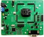
This user's guide describes the 64-pin Sequencer Development Board (UCD90SEQ64EVM-650) for the
following sequencer devices: UCD90120, UCD90124, UCD90120A, UCD90124A, UCD90910, and
UCD90160. This development board contains a 64-pin socket and interface circuitry to support the full line
of 64-pin sequencers.
1
2
3
4
5
6
Contents
Description ................................................................................................................... 2
1.1
Features ............................................................................................................. 2
1.2
Sequencer Applications ........................................................................................... 2
Quick Start ................................................................................................................... 2
2.1
Test Setup .......................................................................................................... 2
UCD90SEQ64EVM-650 GUI Setup ...................................................................................... 3
3.1
UCD90SEQ64EVM-650 GUI Installation ....................................................................... 3
3.2
UCD90SEQ64EVM-650 GUI Operation ........................................................................ 4
General-Use Features ...................................................................................................... 6
4.1
EVM Input/Output Connectors and Switches .................................................................. 6
4.2
EVM Test Jumpers ................................................................................................ 7
4.3
EVM Test Points ................................................................................................... 7
4.4
EVM Status LEDS ................................................................................................. 8
Description ................................................................................................................... 8
5.1
Communication Interface ......................................................................................... 8
5.2
Input Power ......................................................................................................... 9
5.3
Status LED's ........................................................................................................ 9
5.4
Analog Monitor Inputs ............................................................................................. 9
EVM Schematic, Assembly Drawings, Layout Guidelines, and Bill of Materials .................................. 10
6.1
Schematic ......................................................................................................... 10
6.2
PCB Drawings .................................................................................................... 12
6.3
Bill of Materials .................................................................................................... 16
List of Figures
1
Typical Test Setup .......................................................................................................... 3
2
UCD90SEQ64EVM-650 Schematic (Sheet 1 of 2)
3
Figure 3. UCD90SEQ64EVM-650 Schematic (sheet 2 of 2)
4
5
6
7
...................................................................
........................................................
Top-Side Layout/Routing .................................................................................................
Layer-2 Routing ............................................................................................................
Layer-3 Routing ............................................................................................................
Bottom-Side Placement/Routing.........................................................................................
10
11
12
13
14
15
List of Tables
1
Sequencers Summary ...................................................................................................... 2
2
EVM Input/Output Connectors and Switches
3
4
...........................................................................
EVM Jumpers ...............................................................................................................
EVM Test Points ............................................................................................................
SLVU423 – December 2010
Submit Documentation Feedback
UCD90SEQ64EVM-650:— 64-Pin Sequencer Development Board
© 2010, Texas Instruments Incorporated
6
7
7
1
�Description
1
www.ti.com
5
EVM Status LEDS .......................................................................................................... 8
6
UCD90SEQ64EVM-650 Bill of Materials
..............................................................................
16
Description
UCD90SEQ64EVM-650 allows any of TI’s 64-pin sequencers to be installed into the onboard socket for
evaluation. Access to all of the user input/output (I/O) is provided via strip connectors for integration into
complex systems using clip-type jumper wires.
UCD90SEQ64EVM-650 allows direct PMBus (power management bus) communication with the
sequencer via an onboard USB interface. This interface allows direct control of and feedback from the
sequencer when using the TI Fusion Digital Power Designer graphical user interface (GUI).
Table 1. Sequencers Summary
64-Pin (RGC)
Device Part No.
1.1
Number of
Fans
UCD90120
(released)
Generation 1 12-rail sequencer and system health monitor
12 (13 monitor inputs)
10 rails with margining
0
UCD90124
(released)
Generation 1 12-rail sequencer and system health monitor with fan
control
12 (13 monitor inputs)
10 rails with margining
4
UCD90910
(released)
Generation 1+ 10-rail sequencer and system health monitor with fan
control
10 (13 monitor inputs)
10 rails with margining
10
UCD90160
(release in 2011)
Generation 2 16-rail sequencer and system health monitor
16 (16 monitor inputs)
10 rails with margining
0
UCD90120A
(release in 2011)
Generation 2 12-rail sequencer and system health monitor
12 (13 monitor inputs)
10 rails with margining
0
UCD90124A
(release in 2011)
Generation 2 12-rail sequencer and system health monitor with fan
control
12 (13 monitor inputs)
10 rails with margining
4
Features
•
1.2
Number of
Voltage Rails
Description
General Features
– USB port powered or power with single 5-V supply
– JTAG programming port for "in socket" device configuration
– Serial port for advanced debugging
– Status LED’s on all GPIO
– Strip connector I/O access
– USB-PMBus interface for communication
– UCD90124 (in socket) and mini-USB cable provided
Sequencer Applications
•
•
•
•
Industrial/ATE
Telecommunications and networking equipment
Servers and storage systems
Any system requiring sequencing and monitoring of multiple power rails
2
Quick Start
2.1
Test Setup
Figure 1 shows a typical test setup for UCD90SEQ64EVM-650. All that is required is a personal computer
(PC) with a USB port and the TI Fusion Digital Power Designer GUI. The USB-EVM cable is provided with
the EVM and is used for EVM power.
When installing other UCD90xxx sequence devices into XU1, ensure that the device pin 1 is oriented as
shown in Figure 1.
2
UCD90SEQ64EVM-650:— 64-Pin Sequencer Development Board
© 2010, Texas Instruments Incorporated
SLVU423 – December 2010
Submit Documentation Feedback
�UCD90SEQ64EVM-650 GUI Setup
www.ti.com
5 V INPUT
+
-
J5
ADDRESS
J1
J13
5V
Power
Supply
(optional)
J10
J11
LED ENABLE
Device Pin 1
J16
r J15
r J26
D28
USB
J6
J24
J25
J29
JTAG
J20
J19
J23
USB CABLE
J27
XU1 with
UCD90124
Installed
S1
HPA650
J17
J18
RESET
J12
RS 232
PC with GUI
Figure 1. Typical Test Setup
3
UCD90SEQ64EVM-650 GUI Setup
3.1
UCD90SEQ64EVM-650 GUI Installation
The UCD90SEQ64EVM-650 uses the TI Fusion Digital Power Designer GUI which may be downloaded
from the following Web site:
http://focus.ti.com/docs/toolsw/folders/print/fusion_digital_power_designer.html
Click the link for the official release for sequencers to start the download. Place the TI Fusion Digital
Power Designer zip file in a known location on the PC. Unzip the TI Fusion Digital Power Designer zip file.
Double-click the unzipped TI Fusion Digital Power Designer .exe file. Proceed through the installation by
accepting the installer prompts and the license agreement. Accept the GUI-suggested default PC
installation locations to complete the install.
Once the GUI completes the installation, the program starts. The first time the GUI is launched on a
particular PC, the user may be prompted to select a device. Choose UCD9xxx. Afterwards, the GUI may
be closed.
Note that the TI Fusion Digital Power Designer version 1.7.165 was used for the GUI figures in this
document.
SLVU423 – December 2010
Submit Documentation Feedback
UCD90SEQ64EVM-650:— 64-Pin Sequencer Development Board
© 2010, Texas Instruments Incorporated
3
�UCD90SEQ64EVM-650 GUI Setup
3.2
www.ti.com
UCD90SEQ64EVM-650 GUI Operation
The EVM comes preloaded with a 12-rail default project that illuminates the onboard GPIO LED's at power
up. It is a good idea to export the default project to a file on the PC prior to making changes. To do this,
go to the File menu and select Save Project As … then select a project file name and location.
3.2.1
Launch TI Fusion Digital Power Designer
Navigate to the location where the Fusion GUI is installed and (Start, All Programs, Texas Instruments
Fusion Digital Power Designer, Fusion Digital Power Designer), and start it. A window similar to the
following illustration appears.
4
UCD90SEQ64EVM-650:— 64-Pin Sequencer Development Board
© 2010, Texas Instruments Incorporated
SLVU423 – December 2010
Submit Documentation Feedback
�UCD90SEQ64EVM-650 GUI Setup
www.ti.com
Most of the GUI control features are available from the Configure window. Monitor and Status information
is available from the respective buttons on the GUI lower left. A typical Monitor window is follows.
SLVU423 – December 2010
Submit Documentation Feedback
UCD90SEQ64EVM-650:— 64-Pin Sequencer Development Board
© 2010, Texas Instruments Incorporated
5
�General-Use Features
www.ti.com
4
General-Use Features
4.1
EVM Input/Output Connectors and Switches
Table 2. EVM Input/Output Connectors and Switches
Connector/
Label
Switch
J1
+5V POWER
5-V DC jack
J5
+5V
5-V screw jack
J29
USB IN
USB input connector for communication and EVM power
J12
RS232
Serial debug connector
J6
JTAG
JTAG connector
XU1
Onboard socket for the 64-pin sequencer
PBRESET
Pushbutton reset
XU1
S1
6
Description
J18
Sequencer I/O strip connector. Pin name silkscreened on EVM
J21
Sequencer I/O strip connector. Pin name silkscreened on EVM
J23
Sequencer I/O strip connector. Pin name silkscreened on EVM
J24
Sequencer I/O strip connector. Pin name silkscreened on EVM
J20
Sequencer I/O strip connector. Pin name silkscreened on EVM
J17
Sequencer I/O strip connector. Pin name silkscreened on EVM
J11
Sequencer I/O strip connector. Pin name silkscreened on EVM. Unique UCD90160 pin names are
shown on the inside of J11.
J10
Sequencer I/O strip connector. Pin name silkscreened on EVM. Unique UCD90160 pin names are
shown on the inside of J10.
UCD90SEQ64EVM-650:— 64-Pin Sequencer Development Board
© 2010, Texas Instruments Incorporated
SLVU423 – December 2010
Submit Documentation Feedback
�General-Use Features
www.ti.com
4.2
EVM Test Jumpers
The EVM is equipped with shunts on the jumper positions identified in the Default Pin Position shown in
Table 3. Shunts can be moved and removed as required during use.
Table 3. EVM Jumpers
Jumper
Default Pin
Position
Label
J2
1-2
LDO 3.3V
J25
1-2
SCL
EEPROM SCL. For EVM manufacturing only.
J26
1-2
SDA
EEPROM SDA. For EVM manufacturing only.
J9
1-2
GPI1
General purpose input #1. Install shunt to allow status LED operation.
J14
1-2
GPI2
General purpose input #2. Install shunt to allow status LED operation.
J19
1-2
GPI3
General purpose input #3. Install shunt to allow status LED operation.
General purpose input #4. Install shunt to allow status LED operation.
J22
1-2
GPI4
J13
1-2,7-8
PM ADDR
J7
4.3
Description
LDO 3.3V. Install for complete EVM operation. Remove to allow power access to
only the sequencer device.
PMBus address (default to 101). Remove shunts for JTAG operation at address 126.
TCK
JTAG TCK. Install shunt when JTAG operation is desired.
J3
TDI
JTAG TDI. Install shunt when JTAG operation is desired.
J8
TDO
JTAG TDO. Install shunt when JTAG operation is desired.
J4
TMS
JTAG TMS. Install shunt when JTAG operation is desired.
J27
1-2
LEDEN
Status LED enable. Install to enable non-PWM GPIO status LED’s. Remove to
disable status LED loading on the GPIOs.
J28
1-2, 3-4, 5-6, 7-8,
9-10, 11-12,
13-14, 15-16
LEDEN
Status LED enable for FPWMs (GPIO5-GPIO12). Install to enable FPWM GPIO
status LED’s. Remove to disable status LED loading on the FPWM GPIOs.
J15
GPIO14/TX
Debug port TX (used for debug)
J16
GPIO15/RX
Debug port RX (not used during debug)
EVM Test Points
Table 4. EVM Test Points
TP
Color
Label
TP2
WHT
LDO 3.3V
TP1
WHT
V33D
TP5
WHT
ADDR0
ADDRSENS0. EVM PMBus address.
TP6
ORG
ADDR1
ADDRSENS1. EVM PMBus address.
TP3
WHT
RIN
Receive input from terminal device. Connects to GPIO15 through the onboard RS232
transceiver when J16 is installed.
TP4
WHT
TOUT
Transmit output to terminal device. Connects to GPIO14 through the onboard RS232
transceiver when J15 is installed.
TP7
SM-SLV
GND
Surface mount GND
TP8
SM-SLV
GND
Surface mount GND
TP9
SM-SLV
GND
Surface mount GND
TP10
SM-SLV
GND
Surface mount GND
TP11
SM-SLV
GND
Surface mount GND
TP12
SM-SLV
GND
Surface mount GND
SLVU423 – December 2010
Submit Documentation Feedback
Description
LDO 3.3V. EVM 3.3V
V33D. Sequencer 3.3V.
UCD90SEQ64EVM-650:— 64-Pin Sequencer Development Board
© 2010, Texas Instruments Incorporated
7
�Description
4.4
www.ti.com
EVM Status LEDS
Table 5. EVM Status LEDS
5
LED
Color
Label
Description
D5
RED
5V ON
5VBUS ON indicator
Sequencer power ON
D4
RED
V33D
D13
RED
ALERT
D16
GREEN
CTRL
PMBus Control
D28
GREEN
USB ON
USB attached
D6
AMBER
GPI1
GPI1 input HIGH
D7
AMBER
GPI2
GPI2 input HIGH
D8
AMBER
GPI3
GPI3 input HIGH
GPI4 input HIGH
PMBus Alert
D9
AMBER
GPI4
D10
GREEN
GPIO1
GPIO1 HIGH
D11
GREEN
GPIO2
GPIO2 HIGH
D12
GREEN
GPIO3
GPIO3 HIGH
D14
GREEN
GPIO4
GPIO4 HIGH
D15
GREEN
GPIO13
GPIO13 HIGH
D17
GREEN
GPIO14/TX
GPIO14 HIGH
D18
GREEN
GPIO15/RX
GPIO15 HIGH
D19
GREEN
GPIO16
GPIO16 HIGH
D20
GREEN
GPIO17
GPIO17 HIGH
D21
GREEN
GPIO18
GPIO18 HIGH
D22
GREEN
GPIO19
GPIO19 HIGH
D23
GREEN
GPIO20
GPIO20 HIGH
D24
GREEN
GPIO21
GPIO21 HIGH
D25
GREEN
GPIO22
GPIO22 HIGH
D26
AMBER
GPIO5
GPIO5 HIGH
D27
AMBER
GPIO6
GPIO6 HIGH
D29
AMBER
GPIO7
GPIO7 HIGH
D30
AMBER
GPIO8
GPIO8 HIGH
D31
AMBER
GPIO9
GPIO9 HIGH
D32
AMBER
GPIO10
GPIO10 HIGH
D34
AMBER
GPIO11
GPIO11 HIGH
D36
AMBER
GPIO12
GPIO12 HIGH
Description
The following paragraphs describe the UCD90SEQ64EVM-650 functionality and operation.
5.1
Communication Interface
Several communication interfaces to the sequencer are provided on the EVM.
5.1.1
USB Interface
An onboard USB-to-PMBus interface is provided through the USB Input (J29) connector. D28 provides
USB attach status. The EVM can be fully operated from USB input power only.
8
UCD90SEQ64EVM-650:— 64-Pin Sequencer Development Board
© 2010, Texas Instruments Incorporated
SLVU423 – December 2010
Submit Documentation Feedback
�Description
www.ti.com
5.1.2
PMBus
Standard PMBus interface is provided to the sequencer from the onboard USB-PMBus circuitry. PMBus
addressing is set using the J13 jumper block for ADDRSENS1 and ADDRSENS0. respectively. ADDRx =
8 and ADDRx = 5 positions for each are provided. The EVM comes with PMBus address set to 101
decimal.
PMBus Address (decimal) = 12 x ADDR1 + ADDR0 jumper block setting.
5.1.3
JTAG
Standard JTAG programming interface is provided to the sequencer through the J6 connector. The
sequencer address must be set to 126 decimal to invoke sequencer JTAG operation. Install shunts at J3,
J4, J7, and J8, and remove the shunts on J13 to use the JTAG interface.
5.1.4
RS232 Debug
A serial debug port is provided to the sequencer through the J12 connector. Install J15 when using the
RS232 interface. For debug, the terminal listens only to the sequencer.
5.2
Input Power
5VDC EVM input power is provided through the USB interface. For stand-alone operation without a USB
source, EVM input power can be provided at J1 (standard dc jack) or J5 (screw jack). A wall or laptop
adapter with 200-mA capability and 2.5-mm I.D. × 5.5-mm O.D. × 9.5-mm dc jack can power the EVM.
5.3
Status LED's
Visual status information for the GPI, GPIO, and PMBus signals (control and alert) is provided. Logic high
at GPI1-4 or GPIO1-22 illuminates the associated LED. The GPIO status LEDs can be enabled (J27 shunt
installed) or disabled (J27 shunt not installed) to prevent the LED bias from affecting the logic state of the
GPIO signal during device reset. In addition, the sequencer PWM signals PWM1-PWM4 and
FPWM1-FPWM8 can be disconnected from the status LEDs through the use of shunts when used for
voltage margining.
5.4
Analog Monitor Inputs
The sequencer monitor inputs can be used to monitor offboard voltages. Each monitor input has a 4-kΩ
resistor to ground. Ensure that the external source does not exceed 2.5 V.
SLVU423 – December 2010
Submit Documentation Feedback
UCD90SEQ64EVM-650:— 64-Pin Sequencer Development Board
© 2010, Texas Instruments Incorporated
9
�EVM Schematic, Assembly Drawings, Layout Guidelines, and Bill of Materials
www.ti.com
6
EVM Schematic, Assembly Drawings, Layout Guidelines, and Bill of Materials
6.1
Schematic
2
2
2
1
2
1
MON11
MON10
MON9
MON8
MON7
MON16
NC2
MON15
NC1
MON14
MON13
MON12
ADDRSENS0=5
ADDRSENS1=5
ADDRSENS0=8
ADDRSENS1=8
3
5
4
2
3
4
5
Figure 2. UCD90SEQ64EVM-650 Schematic (Sheet 1 of 2)
10
UCD90SEQ64EVM-650:— 64-Pin Sequencer Development Board
SLVU423 – December 2010
Submit Documentation Feedback
© 2010, Texas Instruments Incorporated
�EVM Schematic, Assembly Drawings, Layout Guidelines, and Bill of Materials
www.ti.com
ALERT
CTRL
Figure 3. Figure 3. UCD90SEQ64EVM-650 Schematic (sheet 2 of 2)
SLVU423 – December 2010
Submit Documentation Feedback
UCD90SEQ64EVM-650:— 64-Pin Sequencer Development Board
© 2010, Texas Instruments Incorporated
11
�EVM Schematic, Assembly Drawings, Layout Guidelines, and Bill of Materials
6.2
www.ti.com
PCB Drawings
Figure 4. Top-Side Layout/Routing
12
UCD90SEQ64EVM-650:— 64-Pin Sequencer Development Board
SLVU423 – December 2010
Submit Documentation Feedback
© 2010, Texas Instruments Incorporated
�www.ti.com
EVM Schematic, Assembly Drawings, Layout Guidelines, and Bill of Materials
Figure 5. Layer-2 Routing
SLVU423 – December 2010
Submit Documentation Feedback
UCD90SEQ64EVM-650:— 64-Pin Sequencer Development Board
© 2010, Texas Instruments Incorporated
13
�EVM Schematic, Assembly Drawings, Layout Guidelines, and Bill of Materials
www.ti.com
Figure 6. Layer-3 Routing
14
UCD90SEQ64EVM-650:— 64-Pin Sequencer Development Board
SLVU423 – December 2010
Submit Documentation Feedback
© 2010, Texas Instruments Incorporated
�www.ti.com
EVM Schematic, Assembly Drawings, Layout Guidelines, and Bill of Materials
Figure 7. Bottom-Side Placement/Routing
SLVU423 – December 2010
Submit Documentation Feedback
UCD90SEQ64EVM-650:— 64-Pin Sequencer Development Board
© 2010, Texas Instruments Incorporated
15
�EVM Schematic, Assembly Drawings, Layout Guidelines, and Bill of Materials
6.3
www.ti.com
Bill of Materials
Table 6. UCD90SEQ64EVM-650 Bill of Materials
16
QTY
RefDes
Value
Description
Size
Part Number
MFR
2
C1, C13
4.7uF
Capacitor, Ceramic, 10V, X5R, 20%
0805
Std
Std
1
C12
0.01uF
Capacitor, Ceramic, 50V, X7R, 10%
0603
Std
Std
1
C18
1000pF
Capacitor, Ceramic, X7R, 16V, 10%
0603
Std
Std
1
C2
100uF
Capacitor, Tantalum, 10V, 10%
6032
TAJC107K010R
AVX
2
C20, C21
22pF
Capacitor, Ceramic, 50V, C0G, 10%
0603
Std.
Std.
1
C22
1000pF
Capacitor, Ceramic, 100V, C0G, 5%
0805
Std.
Std.
1
C26
1uF
Capacitor, Tantalum, 16V, 20%
3216
293D105X0016A2T
Vishay
3
C3, C27, C29
10uF
Capacitor, Tantalum, 10V, 20%
3216
293D106X0010A2T
Vishay
18
C4–C11, C14–C17, C19,
C23–C25, C28, C30
0.1uF
Capacitor, Ceramic, X7R, 16V, 10%
0603
Std
Std
1
D1
B340A-13-F
Diode, Schottky, 3A, 40V
SMA
B340A-13-F
Diodes Inc
15
D10–D12, D14–D25
LN1371G
Diode, LED, Green, 20-mA, 0.9-mcd
SMD
LN1371G
Panasonic
1
D2
7.5V
Diode, Zener, 7.5V, 3W
SMB
1SMB5922BT3
On Semi
1
D28
SSF-LXH305GD-TR
Diode, LED, Green, 20 mA, 30 mcd
SMD
SSF-LXH305GD-TR
Lumex
1
D3
TLV1117-33IDCY
IC, Adj., 3.3 V, 800mA LDO Voltage Regulators
SOT-223
TLV1117-33CDCY
TI
1
D33
MBRA130
Diode, Schottky, 1A, 30V
SMA
MBRA130
IR
3
D4, D5, D13
SML-LXT0805SRW-TR
Diode, LED, Red, 100 mA
0805
SML-LXT0805SRW-TR
Lumex
12
D6–D9, D26, D27,
D29–D32, D34, D35
LN1471Y
Diode, LED, Amber, 20-mA, 0.4-mcd
0.114 x 0.049 inch
LN1471YTR
Panasonic
1
FB1
220 Ohm
Ferrite Bead, 2A
0805
BLM21PG221SN
Murata
1
J1
RAPC712X
Connector, DC Jack, Pin dia.2.5mm, Shell dia 5.5mm
0.57 x 0.35 inch
RAPC712X
Switchcraft
8
J10, J11, J17, J18, J20, J21, PEC08SAAN
J23, J24
Header, Male 8-pin, 100mil spacing,
0.100 inch x 8
PEC08SAAN
Sullins
1
J12
182-009-213R171
Connector, 9-pin D, Right Angle, Female
1.213 x 0.510
182-009-213R171
Norcomp
1
J13
PEC04DAAN
Header, Male 2x4-pin, 100mil spacing
0.20 x 0.40 inch
PEC04DAAN
Sullins
14
J2–J4, J7–J9,
J14–J16, J19, J22, J25–J27
PEC02SAAN
Header, Male 2-pin, 100mil spacing,
0.100 inch x 2
PEC02SAAN
Sullins
1
J28
PEC08DAAN
Header, Male 2x8 pin, 100mil spacing
0.100 inch x 2 x 8
PEC08DAAN
Sullins
1
J29
UX60-MB-5ST
Connector, Recpt, USB-B, Mini, 5-pins, SMT
0.354in. x 0.303in.
UX60-MB-5S8
Hirose
1
J5
ED120/2DS
Terminal Block, 2-pin, 15-A, 5.1mm
0.40 x 0.35 inch
ED120/2DS
OST
1
J6
PEC07DAAN
Header, Male 2x7 pin, 100mil spacing
0.100 inch x 2x7
PEC07DAAN
Sullins
1
Q1
FDN5630
MOSFET, N-ch, 60-V,1.7-A, 100-milliohm
SSOT3
FDN5630
Fairchild
5
Q2–Q6
BSS84
Transistor, PFET, -50 V, 130 mA, Rds(ON) < 10 Ω at V(gs) =
5V
SOT-23
BSS84
Fairchild
1
Q7
MMBT2222A
Transistor, NPN, 40 V, 500 mA
SOT-23
MMBT2222A
Fairchild
1
R1
590
Resistor, Chip, 1/10W, 1%
0805
Std
Std
UCD90SEQ64EVM-650:— 64-Pin Sequencer Development Board
SLVU423 – December 2010
Submit Documentation Feedback
© 2010, Texas Instruments Incorporated
�EVM Schematic, Assembly Drawings, Layout Guidelines, and Bill of Materials
www.ti.com
Table 6. UCD90SEQ64EVM-650 Bill of Materials (continued)
QTY
RefDes
Value
Description
Size
Part Number
MFR
27
R12, R14, R22, R35, R43–
R49, R51, R53, R57,
R59–R61, R64, R67, R79,
R81, R87, R90, R92, R93,
R95, R96
332
Resistor, Chip, 1/10W, 1%
0805
Std
Std
10
R13, R15, R24, R37, R58,
R68, R70–R72, R94
100K
Resistor, Chip, 1/16W, 1%
0603
Std
Std
2
R16, R18
84.5K
Resistor, Chip, 1/16W, 1%
0603
Std
Std
2
R17, R19
36.5K
Resistor, Chip, 1/16W, 1%
0603
Std
Std
2
R2, R89
200
Resistor, Chip, 1/16W, 5%
0603
Std
Std
16
R20, R21, R23, R26–R28,
R30–R34, R36, R38–R41
4.02K
Resistor, Chip, 1/16W, 1%
0603
Std
Std
1
R25
20K
Resistor, Chip, 1/16W, 1%
0603
Std
Std
4
R29, R42, R75, R77
1K
Resistor, Chip, 1/16W, 1%
0603
Std
Std
7
R3–R5, R7, R8, R11, R50
10K
Resistor, Chip, 1/16W, 1%
0603
Std
Std
1
R52
300
Resistor, Chip, 1/10W, 1%
0805
Std
Std
1
R54
1.00M
Resistor, Chip, 1/16 W, 1%
0603
Std.
Std.
3
R55, R56, R84
1.5K
Resistor, Chip, 1/16 W, 5%
0603
Std
Std
3
R6, R9, R10
0
Resistor, Chip, 1/16W, 1%
0603
Std
Std
11
R62, R63, R65, R66, R78,
R80, R82, R83, R85, R86,
R88
33
Resistor, Chip, 1/16W, 5%
0603
Std
Std
2
R69, R91
15K
Resistor, Chip, 1/16 W, 5%
0603
Std.
Std
3
R73, R74, R76
2.2K
Resistor, Chip, 1/16 W, 5%
0603
Std.
Std.
1
RT1
5 Ohms
Inrush current limiter, 4.7A, 0.11 Ω
0.180 x 0.550
CL-150
GE Sensing
1
S1
KT11P2JM34LFS
Switch, SPST, PB Momentary, Sealed Washable
0.245 x 0.251
KT11P2JM34LFS
C&K
5
TP1– TP5
5012
Test Point, White, Thru Hole
0.125 x 0.125 inch
5012
Keystone
1
TP6
5013
Test Point, Orange, Thru Hole
0.125 x 0.125 inch
5013
Keystone
6
TP7–TP12
5016
Test Point, SM, 0.150 x 0.090"
0.185 x 0.135
5016
Keystone
2
U1, U3
SN74LVC2G04DBV
IC, Dual Schmitt-Trigger Inverter
SOT23-6
SN74LVC2G04DBV
TI
1
U2
SN75C3221DBR
IC, RS-232 Transceivers with AutoShutdown
SSOP-16
SN75C3221DBR
TI
1
U4
24LC64-I/SN
IC, Serial EEPROM, 64K, 2.5-5.5V,
400 kHz Max.
SO-8
24LC64-I/SN
Microchip
1
U5
TUSB3210PM
IC, USB, General Purpose Device Controller
PQFP-64
TUSB3210PM**
Texas Instruments
1
U6
TPS76333DBV
IC, Micro-Power 100 mA LDO Regulator
SOT23-5
TPS76333DBV
TI
1
XU1
64QN50S19090
Socket, 64-pin Clamshell
0.800 x 1.080 inch
64QN50S19090
Plastronics
1
Y1
12MHZ
Crystal, 12-MHz, 20 pF, ±50 PPM at 25C
0.185 x 0.532
CY12BPSMD
Crystek
1
NA
UCD90124RGC
IC, Digital PWM System Controller with Fan Control
PFC-64
UCD90124RGC
TI
SJ-5003
BUMPON HEMISPHERE 0.44 × 0.20 BLACK
SJ-5003
3M
929950-00
3M
4
18
Shunt, Black
100-mil
SLVU423 – December 2010
Submit Documentation Feedback
UCD90SEQ64EVM-650:— 64-Pin Sequencer Development Board
© 2010, Texas Instruments Incorporated
17
�EVM Schematic, Assembly Drawings, Layout Guidelines, and Bill of Materials
www.ti.com
Table 6. UCD90SEQ64EVM-650 Bill of Materials (continued)
QTY
18
Part Number
MFR
1
RefDes
–
Value
Description
PCB, 5 In x 4 In x 0.062 In
Size
HPA650
Any
1
N/A
USB Cable, 5-pin, B-Mini Male to Type A Male, 2m
AK672M/2-2-R
Assman
UCD90SEQ64EVM-650:— 64-Pin Sequencer Development Board
SLVU423 – December 2010
Submit Documentation Feedback
© 2010, Texas Instruments Incorporated
�Evaluation Board/Kit Important Notice
Texas Instruments (TI) provides the enclosed product(s) under the following conditions:
This evaluation board/kit is intended for use for ENGINEERING DEVELOPMENT, DEMONSTRATION, OR EVALUATION
PURPOSES ONLY and is not considered by TI to be a finished end-product fit for general consumer use. Persons handling the
product(s) must have electronics training and observe good engineering practice standards. As such, the goods being provided are
not intended to be complete in terms of required design-, marketing-, and/or manufacturing-related protective considerations,
including product safety and environmental measures typically found in end products that incorporate such semiconductor
components or circuit boards. This evaluation board/kit does not fall within the scope of the European Union directives regarding
electromagnetic compatibility, restricted substances (RoHS), recycling (WEEE), FCC, CE or UL, and therefore may not meet the
technical requirements of these directives or other related directives.
Should this evaluation board/kit not meet the specifications indicated in the User’s Guide, the board/kit may be returned within 30
days from the date of delivery for a full refund. THE FOREGOING WARRANTY IS THE EXCLUSIVE WARRANTY MADE BY
SELLER TO BUYER AND IS IN LIEU OF ALL OTHER WARRANTIES, EXPRESSED, IMPLIED, OR STATUTORY, INCLUDING
ANY WARRANTY OF MERCHANTABILITY OR FITNESS FOR ANY PARTICULAR PURPOSE.
The user assumes all responsibility and liability for proper and safe handling of the goods. Further, the user indemnifies TI from all
claims arising from the handling or use of the goods. Due to the open construction of the product, it is the user’s responsibility to
take any and all appropriate precautions with regard to electrostatic discharge.
EXCEPT TO THE EXTENT OF THE INDEMNITY SET FORTH ABOVE, NEITHER PARTY SHALL BE LIABLE TO THE OTHER
FOR ANY INDIRECT, SPECIAL, INCIDENTAL, OR CONSEQUENTIAL DAMAGES.
TI currently deals with a variety of customers for products, and therefore our arrangement with the user is not exclusive.
TI assumes no liability for applications assistance, customer product design, software performance, or infringement of
patents or services described herein.
Please read the User’s Guide and, specifically, the Warnings and Restrictions notice in the User’s Guide prior to handling the
product. This notice contains important safety information about temperatures and voltages. For additional information on TI’s
environmental and/or safety programs, please contact the TI application engineer or visit www.ti.com/esh.
No license is granted under any patent right or other intellectual property right of TI covering or relating to any machine, process, or
combination in which such TI products or services might be or are used.
FCC Warning
This evaluation board/kit is intended for use for ENGINEERING DEVELOPMENT, DEMONSTRATION, OR EVALUATION
PURPOSES ONLY and is not considered by TI to be a finished end-product fit for general consumer use. It generates, uses, and
can radiate radio frequency energy and has not been tested for compliance with the limits of computing devices pursuant to part 15
of FCC rules, which are designed to provide reasonable protection against radio frequency interference. Operation of this
equipment in other environments may cause interference with radio communications, in which case the user at his own expense
will be required to take whatever measures may be required to correct this interference.
EVM Warnings and Restrictions
It is important to operate this EVM within the input voltage range of 0 V to 5.5 V and the output voltage range of 0 V to 3.8 V .
Exceeding the specified input range may cause unexpected operation and/or irreversible damage to the EVM. If there are
questions concerning the input range, please contact a TI field representative prior to connecting the input power.
Applying loads outside of the specified output range may result in unintended operation and/or possible permanent damage to the
EVM. Please consult the EVM User's Guide prior to connecting any load to the EVM output. If there is uncertainty as to the load
specification, please contact a TI field representative.
During normal operation, some circuit components may have case temperatures greater than 40° C. The EVM is designed to
operate properly with certain components above 70° C as long as the input and output ranges are maintained. These components
include but are not limited to linear regulators, switching transistors, pass transistors, and current sense resistors. These types of
devices can be identified using the EVM schematic located in the EVM User's Guide. When placing measurement probes near
these devices during operation, please be aware that these devices may be very warm to the touch.
Mailing Address: Texas Instruments, Post Office Box 655303, Dallas, Texas 75265
Copyright © 2010, Texas Instruments Incorporated
�IMPORTANT NOTICE
Texas Instruments Incorporated and its subsidiaries (TI) reserve the right to make corrections, modifications, enhancements, improvements,
and other changes to its products and services at any time and to discontinue any product or service without notice. Customers should
obtain the latest relevant information before placing orders and should verify that such information is current and complete. All products are
sold subject to TI’s terms and conditions of sale supplied at the time of order acknowledgment.
TI warrants performance of its hardware products to the specifications applicable at the time of sale in accordance with TI’s standard
warranty. Testing and other quality control techniques are used to the extent TI deems necessary to support this warranty. Except where
mandated by government requirements, testing of all parameters of each product is not necessarily performed.
TI assumes no liability for applications assistance or customer product design. Customers are responsible for their products and
applications using TI components. To minimize the risks associated with customer products and applications, customers should provide
adequate design and operating safeguards.
TI does not warrant or represent that any license, either express or implied, is granted under any TI patent right, copyright, mask work right,
or other TI intellectual property right relating to any combination, machine, or process in which TI products or services are used. Information
published by TI regarding third-party products or services does not constitute a license from TI to use such products or services or a
warranty or endorsement thereof. Use of such information may require a license from a third party under the patents or other intellectual
property of the third party, or a license from TI under the patents or other intellectual property of TI.
Reproduction of TI information in TI data books or data sheets is permissible only if reproduction is without alteration and is accompanied
by all associated warranties, conditions, limitations, and notices. Reproduction of this information with alteration is an unfair and deceptive
business practice. TI is not responsible or liable for such altered documentation. Information of third parties may be subject to additional
restrictions.
Resale of TI products or services with statements different from or beyond the parameters stated by TI for that product or service voids all
express and any implied warranties for the associated TI product or service and is an unfair and deceptive business practice. TI is not
responsible or liable for any such statements.
TI products are not authorized for use in safety-critical applications (such as life support) where a failure of the TI product would reasonably
be expected to cause severe personal injury or death, unless officers of the parties have executed an agreement specifically governing
such use. Buyers represent that they have all necessary expertise in the safety and regulatory ramifications of their applications, and
acknowledge and agree that they are solely responsible for all legal, regulatory and safety-related requirements concerning their products
and any use of TI products in such safety-critical applications, notwithstanding any applications-related information or support that may be
provided by TI. Further, Buyers must fully indemnify TI and its representatives against any damages arising out of the use of TI products in
such safety-critical applications.
TI products are neither designed nor intended for use in military/aerospace applications or environments unless the TI products are
specifically designated by TI as military-grade or "enhanced plastic." Only products designated by TI as military-grade meet military
specifications. Buyers acknowledge and agree that any such use of TI products which TI has not designated as military-grade is solely at
the Buyer's risk, and that they are solely responsible for compliance with all legal and regulatory requirements in connection with such use.
TI products are neither designed nor intended for use in automotive applications or environments unless the specific TI products are
designated by TI as compliant with ISO/TS 16949 requirements. Buyers acknowledge and agree that, if they use any non-designated
products in automotive applications, TI will not be responsible for any failure to meet such requirements.
Following are URLs where you can obtain information on other Texas Instruments products and application solutions:
Products
Applications
Amplifiers
amplifier.ti.com
Audio
www.ti.com/audio
Data Converters
dataconverter.ti.com
Automotive
www.ti.com/automotive
DLP® Products
www.dlp.com
Communications and
Telecom
www.ti.com/communications
DSP
dsp.ti.com
Computers and
Peripherals
www.ti.com/computers
Clocks and Timers
www.ti.com/clocks
Consumer Electronics
www.ti.com/consumer-apps
Interface
interface.ti.com
Energy
www.ti.com/energy
Logic
logic.ti.com
Industrial
www.ti.com/industrial
Power Mgmt
power.ti.com
Medical
www.ti.com/medical
Microcontrollers
microcontroller.ti.com
Security
www.ti.com/security
RFID
www.ti-rfid.com
Space, Avionics &
Defense
www.ti.com/space-avionics-defense
RF/IF and ZigBee® Solutions www.ti.com/lprf
Video and Imaging
www.ti.com/video
Wireless
www.ti.com/wireless-apps
Mailing Address: Texas Instruments, Post Office Box 655303, Dallas, Texas 75265
Copyright © 2010, Texas Instruments Incorporated
�