Sample &
Buy
Product
Folder
Support &
Community
Tools &
Software
Technical
Documents
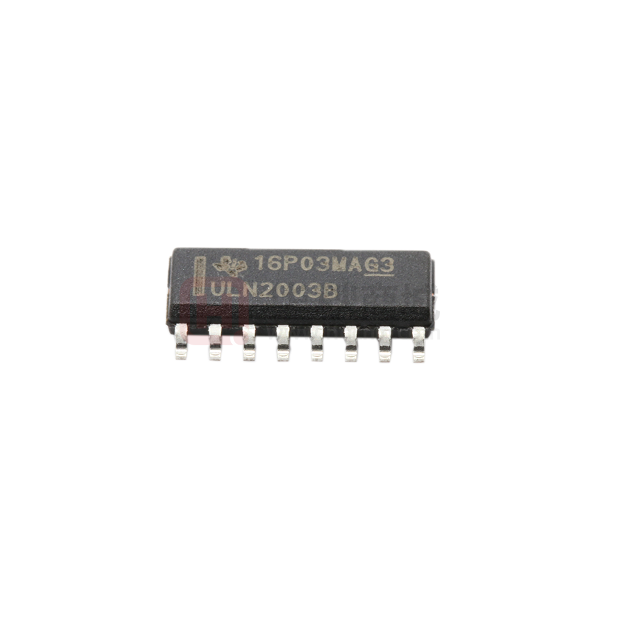
ULN2003B
SLRS064B – JUNE 2014 – REVISED AUGUST 2016
ULN2003B High-Voltage, High-Current Darlington Transistor Array
1 Features
3 Description
•
The ULN2003B device is a high-voltage, high-current
Darlington transistor array. This device consists of
seven NPN Darlington pairs that feature high-voltage
outputs with common-cathode clamp diodes for
switching inductive loads. The collector-current rating
of a single Darlington pair is 500 mA. The Darlington
pairs can be paralleled for higher current capability.
1
•
•
•
•
•
Greater Than 4x Reduction in Output Leakage
(ICEX) over ULN2003A
500-mA Rated Collector Current (Single Output)
High-Voltage Outputs 50 V
Output Clamp Diodes
Inputs Compatible With Various Types of Logic
Relay-Driver Applications
2 Applications
•
•
•
•
•
Relay Drivers
Lamp Drivers
Display Drivers (LED and Gas Discharge)
Line Drivers
Logic Buffers
The ULN2003B has a 2.7-kΩ series base resistor for
each Darlington pair for operation directly with TTL or
CMOS devices.
Device Information(1)
PART NUMBER
PACKAGE
BODY SIZE (NOM)
ULN2003BN
PDIP (16)
19.30 mm × 6.35 mm
ULN2003BD
SOIC (16)
9.90 mm × 3.91 mm
ULN2003BPW
TSSOP (16)
5.00 mm × 4.40 mm
(1) For all available packages, see the orderable addendum at
the end of the datasheet.
Simplified Schematic
9
COM
1
16
1B
1C
2
15
2B
2C
3
14
3B
3C
4
13
4B
4C
5
12
5C
5B
6
11
7
10
6B
7B
6C
7C
Copyright © 2016, Texas Instruments Incorporated
1
An IMPORTANT NOTICE at the end of this data sheet addresses availability, warranty, changes, use in safety-critical applications,
intellectual property matters and other important disclaimers. PRODUCTION DATA.
�ULN2003B
SLRS064B – JUNE 2014 – REVISED AUGUST 2016
www.ti.com
Table of Contents
1
2
3
4
5
6
7
8
Features ..................................................................
Applications ...........................................................
Description .............................................................
Revision History.....................................................
Pin Configuration and Functions .........................
Specifications.........................................................
1
1
1
2
3
4
6.1
6.2
6.3
6.4
6.5
6.6
6.7
6.8
6.9
4
4
4
4
5
5
5
5
6
Absolute Maximum Ratings ......................................
ESD Ratings..............................................................
Recommended Operating Conditions.......................
Thermal Information ..................................................
Electrical Characteristics, TA = 25°C .......................
Electrical Characteristics, TA = –40°C to +105°C ....
Switching Characteristics, TA = 25°C........................
Switching Characteristics, TA = –40°C to +105°C ....
Typical Characteristics ..............................................
Parameter Measurement Information .................. 9
Detailed Description ............................................ 10
8.1 Overview ................................................................. 10
8.2 Functional Block Diagram ....................................... 10
8.3 Feature Description................................................. 10
8.4 Device Functional Modes........................................ 11
9
Application and Implementation ........................ 11
9.1 Application Information............................................ 11
9.2 Typical Application ................................................. 11
10 Power Supply Recommendations ..................... 13
11 Layout................................................................... 13
11.1 Layout Guidelines ................................................. 13
11.2 Layout Example .................................................... 13
12 Device and Documentation Support ................. 14
12.1
12.2
12.3
12.4
12.5
Receiving Notification of Documentation Updates
Community Resources..........................................
Trademarks ...........................................................
Electrostatic Discharge Caution ............................
Glossary ................................................................
14
14
14
14
14
13 Mechanical, Packaging, and Orderable
Information ........................................................... 14
4 Revision History
Changes from Revision A (September 2014) to Revision B
Page
•
Deleted Hammer Drivers from Applications ........................................................................................................................... 1
•
Updated Pin Functions table .................................................................................................................................................. 3
•
Deleted Package Themal Information from Absolute Maximum Ratings ............................................................................... 4
•
Moved Storage temperature, Tstg to Absolute Maximum Ratings .......................................................................................... 4
•
Deleted VI from Recommended Operating Conditions........................................................................................................... 4
•
Updated Thermal Information table ....................................................................................................................................... 4
•
Moved Operating free-air temperature, TA to Recommended Operating Conditions............................................................. 4
•
Deleted Output Current vs Input Current graph from Typical Characteristics section ........................................................... 6
•
Added hFE vs IOUT to Typical Characteristics section.............................................................................................................. 6
•
Deleted Thermal Information graphs section and updated Typical Characteristics section with new thermal graphs
Figure 6 through Figure 14 ..................................................................................................................................................... 6
•
Added Receiving Notification of Documentation Updates section and Community Resources section .............................. 14
Changes from Original (June 2014) to Revision A
Page
•
Initial release of full version. .................................................................................................................................................. 1
•
Added Pin Functions table...................................................................................................................................................... 3
•
Added Thermal Information table. .......................................................................................................................................... 4
2
Submit Documentation Feedback
Copyright © 2014–2016, Texas Instruments Incorporated
Product Folder Links: ULN2003B
�ULN2003B
www.ti.com
SLRS064B – JUNE 2014 – REVISED AUGUST 2016
5 Pin Configuration and Functions
D, N, or PW Package
16-Pin SOIC, PDIP, or TSSOP
Top View
1B
1
16
1C
2B
2
15
2C
3B
3
14
3C
4B
4
13
4C
5B
5
12
5C
6B
6
11
6C
7B
7
10
7C
E
8
9
COM
Not to scale
Pin Functions
PIN
NAME
NO.
1B
1
2B
2
3B
3
4B
4
5B
5
6B
6
7B
7
1C
16
2C
15
3C
14
4C
13
5C
12
6C
11
7C
10
COM
E
(1)
I/O (1)
DESCRIPTION
I
Channel 1 through 7 darlington base input
O
Channel 1 through 7 darlington collector output
9
—
Common cathode node for flyback diodes (required for inductive loads)
8
—
Common Emmitter shared by all channels (typically tied to ground)
I = Input, O = Output
Submit Documentation Feedback
Copyright © 2014–2016, Texas Instruments Incorporated
Product Folder Links: ULN2003B
3
�ULN2003B
SLRS064B – JUNE 2014 – REVISED AUGUST 2016
www.ti.com
6 Specifications
6.1 Absolute Maximum Ratings
at 25°C free-air temperature (unless otherwise noted) (1)
MIN
VCC
VI
MAX
UNIT
Collector-emitter voltage
50
V
Clamp diode reverse voltage (2)
50
V
Input voltage
(2)
30
V
500
mA
Output clamp current
500
mA
Total emitter-terminal current
–2.5
A
150
°C
150
°C
Peak collector current (3) (4)
IOK
TJ
Operating virtual junction temperature
Tstg
Storage temperature
(1)
(2)
(3)
(4)
–65
Stresses beyond those listed under Absolute Maximum Ratings may cause permanent damage to the device. These are stress ratings
only, which do not imply functional operation of the device at these or any other conditions beyond those indicated under Recommended
Operating Conditions. Exposure to absolute-maximum-rated conditions for extended periods may affect device reliability.
All voltage values are with respect to the emitter/substrate terminal E, unless otherwise noted.
Maximum power dissipation is a function of TJ(max), θJA, and TA. The maximum allowable power dissipation at any allowable ambient
temperature is PD = (TJ(max) – TA)/θJA. Operating at the absolute maximum TJ of 150°C can affect reliability.
The package thermal impedance is calculated in accordance with JESD 51-7.
6.2 ESD Ratings
VALUE
V(ESD)
(1)
(2)
Electrostatic discharge
Human body model (HBM), per ANSI/ESDA/JEDEC JS-001 (1)
2000
Charged device model (CDM), per JEDEC specification JESD22-C101 (2)
500
UNIT
V
JEDEC document JEP155 states that 500-V HBM allows safe manufacturing with a standard ESD control process.
JEDEC document JEP157 states that 250-V CDM allows safe manufacturing with a standard ESD control process.
6.3 Recommended Operating Conditions
over operating free-air temperature range (unless otherwise noted)
MIN
MAX
UNIT
VCC
Supply Voltage
0
50
V
TA
Operating free-air temperature
–40
105
°C
TJ
Junction Temperature
–40
125
°C
6.4 Thermal Information
ULN2003B
THERMAL METRIC
(1)
PW (TSSOP)
D (SOIC)
N (PDIP)
16 PINS
16 PINS
16 PINS
UNIT
RθJA
Junction-to-ambient thermal resistance
105.5
81.2
49.6
°C/W
RθJC(top)
Junction-to-case (top) thermal resistance
38.3
40
36.2
°C/W
RθJB
Junction-to-board thermal resistance
50.9
38.6
29.2
°C/W
ψJT
Junction-to-top characterization parameter
4.1
10.5
20.2
°C/W
ψJB
Junction-to-board characterization parameter
50.3
38.3
29.5
°C/W
(1)
4
For more information about traditional and new thermal metrics, see the Semiconductor and IC Package Thermal Metrics application
report.
Submit Documentation Feedback
Copyright © 2014–2016, Texas Instruments Incorporated
Product Folder Links: ULN2003B
�ULN2003B
www.ti.com
SLRS064B – JUNE 2014 – REVISED AUGUST 2016
6.5 Electrical Characteristics, TA = 25°C
PARAMETER
VI(on)
VCE(sat)
On-state input voltage
Collector-emitter saturation
voltage
TEST FIGURE
Figure 19
Figure 18
TEST CONDITIONS
VCE = 2 V
2.7
3
II = 500 μA,
II = 0
VCE = 50 V,
VF
Clamp forward voltage
Figure 21
IF = 350 mA
II(off)
Off-state input current
Figure 16
VCE = 50 V,
II
Input current
Figure 17
VI = 3.85 V
IR
Clamp reverse current
Figure 20
VR = 50 V
Ci
Input capacitance
VI = 0,
UNIT
IC = 300 mA
II = 350 μA,
Figure 15
MAX
IC = 250 mA
IC = 100 mA
Collector cutoff current
TYP
2.4
II = 250 μA,
ICEX
MIN
IC = 200 mA
0.9
1.1
IC = 200 mA
1
1.3
IC = 350 mA
1.2
1.6
10
1.7
IC = 500 μA
50
2
65
V
μA
V
μA
0.93
f = 1 MHz
V
1.35
mA
50
μA
25
pF
15
6.6 Electrical Characteristics, TA = –40°C to +105°C
PARAMETER
VI(on)
VCE(sat)
On-state input voltage
Collector-emitter saturation voltage
TEST FIGURE
Figure 19
Figure 18
TEST CONDITIONS
VCE = 2 V
2.9
IC = 300 mA
3
II = 500 μA,
II = 0
VCE = 50 V,
VF
Clamp forward voltage
Figure 21
IF = 350 mA
II(off)
Off-state input current
Figure 16
VCE = 50 V,
II
Input current
Figure 17
VI = 3.85 V
IR
Clamp reverse current
Figure 20
VR = 50 V
Ci
Input capacitance
VI = 0,
UNIT
2.7
II = 350 μA,
Figure 15
MAX
IC = 250 mA
IC = 100 mA
Collector cutoff current
TYP
IC = 200 mA
II = 250 μA,
ICEX
MIN
0.9
1.2
IC = 200 mA
1
1.4
IC = 350 mA
1.2
1.7
V
20
1.7
IC = 500 μA
V
30
2.2
V
65
μA
0.93
f = 1 MHz
μA
15
1.35
mA
100
μA
25
pF
6.7 Switching Characteristics, TA = 25°C
PARAMETER
TEST CONDITIONS
MIN
TYP
MAX
tPLH
Propagation delay time, low- to high-level output
0.25
1
tPHL
Propagation delay time, high- to low-level output
0.25
1
VOH
High-level output voltage after switching
VS = 50 V,
IO ≈ 300 mA
VS – 20
UNIT
μs
μs
mV
6.8 Switching Characteristics, TA = –40°C to +105°C
PARAMETER
TEST CONDITIONS
MIN
TYP
MAX
tPLH
Propagation delay time, low- to high-level output
1
10
tPHL
Propagation delay time, high- to low-level output
1
10
VOH
High-level output voltage after switching
VS = 50 V,
IO ≈ 300 mA
VS – 50
Submit Documentation Feedback
Copyright © 2014–2016, Texas Instruments Incorporated
Product Folder Links: ULN2003B
UNIT
μs
μs
mV
5
�ULN2003B
SLRS064B – JUNE 2014 – REVISED AUGUST 2016
www.ti.com
2.2
Iin = 250uA
Iin = 350uA
Iin = 500uA
2
1.8
1.6
1.4
1.2
1
0.8
0.6
0.4
0
50
100
150 200 250 300 350
IC- Collector Current - mA
400
450
500
VCE(sat) - Collector-Emitter Saturation Voltage - V
VCE(sat) - Collector-Emitter Saturation Voltage - V
6.9 Typical Characteristics
Iin = 250uA
Iin = 350uA
Iin = 500uA
1.5
1.35
1.2
1.05
0.9
0.75
0.6
0.45
0
80
160
D001
240 320 400 480 560
IC- Collector Current - mA
640
720
800
D001
Figure 1. Collector-Emitter Saturation Voltage vs Collector
Current (One Darlington)
Figure 2. Collector-Emitter Saturation Voltage vs Total
Collector Current (Two Darlingtons in Parallel)
Figure 3. Input Current vs Input Voltage
Figure 4. Collector-Emitter Saturation Voltage vs Collector
Current
5000
0.55
3000
2000
Maximum Current per Channel (A)
DC Current Transfer Ratio - h FE
1.8
1.65
1000
500
300
200
100
50
TA = 25 qC
TA = -40 qC
TA = 105 qC
30
20
10
1 mA
0.5
0.45
0.4
0.35
0.3
0.25
1 Ch
2 Ch
3 Ch
4 Ch
5 Ch
6 Ch
7 Ch
0.2
0.15
0.1
0.05
0
10 mA
100 mA
Output Current IOUT
500 mA
0
20%
D001
40%
60%
Duty Cycle (DC)
80%
100%
D001
TA = 25ºC
Figure 5. hFE vs IOUT
6
Figure 6. D Package Maximum Collector Current
vs Duty Cycle
Submit Documentation Feedback
Copyright © 2014–2016, Texas Instruments Incorporated
Product Folder Links: ULN2003B
�ULN2003B
www.ti.com
SLRS064B – JUNE 2014 – REVISED AUGUST 2016
Typical Characteristics (continued)
0.55
0.5
Maximum Current per Channel (A)
Maximum Current per Channel (A)
0.55
0.45
0.4
0.35
0.3
0.25
1 Ch
2 Ch
3 Ch
4 Ch
5 Ch
6 Ch
7 Ch
0.2
0.15
0.1
0.05
0
0.5
0.45
0.4
0.35
0.3
0.25
1 Ch
2 Ch
3 Ch
4 Ch
5 Ch
6 Ch
7 Ch
0.2
0.15
0.1
0.05
0
0
20%
40%
60%
Duty Cycle (DC)
80%
100%
0
20%
D001
40%
60%
Duty Cycle (DC)
TA = 25ºC
D001
Figure 8. N Package Maximum Collector Current
vs Duty Cycle
0.55
0.55
0.5
Maximum Current per Channel (A)
Maximum Current per Channel (A)
100%
TA = 25ºC
Figure 7. PW Package Maximum Collector Current
vs Duty Cycle
0.45
0.4
0.35
0.3
0.25
1 Ch
2 Ch
3 Ch
4 Ch
5 Ch
6 Ch
7 Ch
0.2
0.15
0.1
0.05
0.5
0.45
0.4
0.35
0.3
0.25
0.2
0.15
1 Ch
2 Ch
3 Ch
4 Ch
0.1
0.05
5 Ch
6 Ch
7 Ch
0
0
0
0.1
0.2
0.3
0.4 0.5 0.6
Duty Cycle (DC)
0.7
0.8
0.9
0
1
20%
D001
TA = 70ºC
0.5
Maximum Current per Channel (A)
0.55
0.5
0.45
0.4
0.35
0.3
1 Ch
2 Ch
3 Ch
4 Ch
5 Ch
6 Ch
7 Ch
0.2
0.15
0.1
0.05
80%
100%
D001
Figure 10. PW Package Maximum Collector Current
vs Duty Cycle
0.55
0.25
40%
60%
Duty Cycle (DC)
TA = 70ºC
Figure 9. D Package Maximum Collector Current
vs Duty Cycle
Maximum Current per Channel (A)
80%
1 Ch
2 Ch
3 Ch
4 Ch
5 Ch
6 Ch
7 Ch
0.45
0.4
0.35
0.3
0.25
0.2
0.15
0.1
0.05
0
0
0
20%
40%
60%
Duty Cycle (DC)
80%
100%
0
D001
TA = 70ºC
20%
40%
60%
Duty Cycle (DC)
80%
100%
D001
TA = 105ºC
Figure 11. N Package Maximum Collector Current
vs Duty Cycle
Figure 12. D Package Maximum Collector Current
vs Duty Cycle
Submit Documentation Feedback
Copyright © 2014–2016, Texas Instruments Incorporated
Product Folder Links: ULN2003B
7
�ULN2003B
SLRS064B – JUNE 2014 – REVISED AUGUST 2016
www.ti.com
Typical Characteristics (continued)
0.55
1 Ch
2 Ch
3 Ch
4 Ch
5 Ch
6 Ch
7 Ch
0.5
0.45
0.4
0.35
0.3
Maximum Current per Channel (A)
Maximum Current per Channel (A)
0.55
0.25
0.2
0.15
0.1
0.05
0
1 Ch
2 Ch
3 Ch
4 Ch
0.5
0.45
0.4
0.35
0.3
0.25
0.2
0.15
0.1
0.05
0
0
20%
40%
60%
Duty Cycle (DC)
80%
100%
0
D001
TA = 105ºC
20%
40%
60%
Duty Cycle (DC)
80%
100%
D001
TA = 105ºC
Figure 13. PW Package Maximum Collector Current
vs Duty Cycle
8
5 Ch
6 Ch
7 Ch
Figure 14. N Package Maximum Collector Current vs Duty
Cycle
Submit Documentation Feedback
Copyright © 2014–2016, Texas Instruments Incorporated
Product Folder Links: ULN2003B
�ULN2003B
www.ti.com
SLRS064B – JUNE 2014 – REVISED AUGUST 2016
7 Parameter Measurement Information
Open
Open
V CE
V CE
II(off)
ICEX
IC
Open
Figure 15. ICEX Test Circuit
Figure 16. II(off) Test Circuit
Open
Open
II(on)
h FE =
Open
VI
VCE
II
Figure 17. II Test Circuit
IC
II
IC
Figure 18. hfe , VCE(sat) Test Circuit
VR
Open
IR
Open
V I(o n)
V CE
IC
Figure 19. VI(on) Test Circuit
Figure 20. IR Test Circuit
VF
IF
Open
Figure 21. VF Test Circuit
Submit Documentation Feedback
Copyright © 2014–2016, Texas Instruments Incorporated
Product Folder Links: ULN2003B
9
�ULN2003B
SLRS064B – JUNE 2014 – REVISED AUGUST 2016
www.ti.com
8 Detailed Description
8.1 Overview
This standard device has proven ubiquity and versatility across a wide range of applications. This is due to it's
integration of 7 Darlington transistors that are capable of sinking up to 500 mA and wide GPIO range capability.
The ULN2003B comprises seven high voltage, high current NPN Darlington transistor pairs. All units feature a
common emitter and open collector outputs. To maximize their effectiveness, these units contain suppression
diodes for inductive loads. The ULN2003B has a series base resistor to each Darlington pair, thus allowing
operation directly with TTL or CMOS operating at supply voltages of 5 V or 3.3 V. The ULN2003B offers
solutions to a great many interface needs, including solenoids, relays, lamps, small motors, and LEDs.
Applications requiring sink currents beyond the capability of a single output may be accommodated by paralleling
the outputs.
This device can operate over a wide temperature range (–40°C to +105°C).
8.2 Functional Block Diagram
COM
Output C
2 .7 k
Input B
7.2 k
3k
E
Copyright © 2016, Texas Instruments Incorporated
All resistor values shown are nominal.
Figure 22. Schematic (Each Driver)
8.3 Feature Description
Each channel of ULN2003B consists of Darlington connected NPN transistors. This connection creates the effect
of a single transistor with a very high current gain. This beta can be high at certain currents see Figure 5.
The GPIO voltage is converted to base current through the 2.7-kΩ resistor connected between the input and
base of the pre-driver Darlington NPN. The 7.2-kΩ and 3-kΩ resistors connected between the base and emitter
of each respective NPN act as pull-downs and suppress the amount of leakage that may occur from the input.
The diodes connected between the output and COM pin is used to suppress the kick-back voltage from an
inductive load that is excited when the NPN drivers are turned off (stop sinking) and the stored energy in the
coils causes a reverse current to flow into the coil supply through the kick-back diode.
In normal operation the diodes on base and collector pins to emitter will be reversed biased. If these diode are
forward biased, internal parasitic NPN transistors will draw (a nearly equal) current from other (nearby) device
pins.
10
Submit Documentation Feedback
Copyright © 2014–2016, Texas Instruments Incorporated
Product Folder Links: ULN2003B
�ULN2003B
www.ti.com
SLRS064B – JUNE 2014 – REVISED AUGUST 2016
8.4 Device Functional Modes
8.4.1 Inductive Load Drive
When the COM pin is tied to the coil supply voltage, ULN2003B is able to drive inductive loads and suppress the
kick-back voltage through the internal free wheeling diodes.
8.4.2 Resistive Load Drive
When driving a resistive load, a pull-up resistor is needed in order for ULN2003B to sink current and for there to
be a logic high level. The COM pin can be left floating for these applications.
9 Application and Implementation
NOTE
Information in the following applications sections is not part of the TI component
specification, and TI does not warrant its accuracy or completeness. TI’s customers are
responsible for determining suitability of components for their purposes. Customers should
validate and test their design implementation to confirm system functionality.
9.1 Application Information
ULN2003B will typically be used to drive a high voltage and/or current peripheral from an MCU or logic device
that cannot tolerate these conditions. The following design is a common application of ULN2003B, driving
inductive loads. This includes motors, solenoids and relays. Figure 23 is a typical block diagram representation of
this application.
9.2 Typical Application
VSUP
ULN2003B
3.3V Logic
3.3V Logic
3.3V Logic
IN1
OUT1
IN2
OUT2
IN3
OUT3
IN4
OUT4
IN5
OUT5
IN6
OUT6
IN7
OUT7
GND
VSUP
COM
Copyright © 2016, Texas Instruments Incorporated
Figure 23. ULN2003B as Inductive Load Driver
Submit Documentation Feedback
Copyright © 2014–2016, Texas Instruments Incorporated
Product Folder Links: ULN2003B
11
�ULN2003B
SLRS064B – JUNE 2014 – REVISED AUGUST 2016
www.ti.com
Typical Application (continued)
9.2.1 Design Requirements
For this design example, use the parameters listed in Table 1 as the input parameters.
Table 1. Design Parameters
DESIGN PARAMETER
(1)
(1)
EXAMPLE VALUE
GPIO Voltage
3.3 V or 5 V
Coil Supply Voltage
12 V to 48 V
Number of Channels
7
Output Current (RCOIL)
20 mA to 300 mA per channel (See Figure 5)
Duty Cycle
See Figure 6 to Figure 14
These test conditions can not be run simultaneously.
9.2.2 Detailed Design Procedure
When using ULN2003B in a coil driving application, determine the following:
• Input Voltage Range
• Temperature Range
• Output and Drive Current
• Power Dissipation
9.2.2.1 Drive Current
The coil current is determined by the coil voltage (VSUP), coil resistance and output low voltage (VOL or
VCE(SAT)).
ICOIL = (VSUP – VCE(SAT)) / RCOIL
(1)
9.2.2.2 Output Low Voltage
The output low voltage (VOL) is the same thing as VCE(SAT) and can be determined by, Figure 1, Figure 2, or
Figure 4.
9.2.2.3 Power Dissipation and Temperature
The number of coils driven is dependent on the coil current and on-chip power dissipation. The number of coils
driven can be determined by Figure 6 or Figure 7.
For a more accurate determination of number of coils possible, use Equation 2 to calculate ULN2003B on-chip
power dissipation PD:
N
PD = å VOLi ´ ILi
i=1
where
•
•
N is the number of channels active together.
VOLi is the OUTi pin voltage for the load current ILi. This is the same as VCE(SAT)
(2)
In order to guarantee reliability of ULN2003B and the system the on-chip power dissipation must be lower that or
equal to the maximum allowable power dissipation (PD(MAX)) dictated by Equation 3.
PD(MAX) =
(T
J(MAX)
- TA )
qJA
where
•
•
•
12
TJ(MAX) is the target maximum junction temperature.
TA is the operating ambient temperature.
θJA is the package junction to ambient thermal resistance.
Submit Documentation Feedback
(3)
Copyright © 2014–2016, Texas Instruments Incorporated
Product Folder Links: ULN2003B
�ULN2003B
www.ti.com
SLRS064B – JUNE 2014 – REVISED AUGUST 2016
TI recommends to limit ULN2003B IC’s die junction temperature to less than 125°C. The IC junction temperature
is directly proportional to the on-chip power dissipation.
9.2.3 Application Curves
14
13
12
11
10
9
8
7
6
5
4
3
2
1
0
-0.004
12
Output voltage - V
Output voltage - V
The following curves were generated with ULN2003B driving an OMRON G5NB relay – Vin = 5.0V; Vsup= 12 V
and RCOIL= 2.8 kΩ
10
8
6
4
2
0
0.004
0.008
Time (s)
0.012
0
-0.004
0.016
D001
Figure 24. Output Response With Activation
of Coil (Turn On)
0
0.004
0.008
Time (s)
0.012
0.016
D001
Figure 25. Output Response With De-activation
of Coil (Turn Off)
10 Power Supply Recommendations
This part does not need a power supply; however, the COM pin is typically tied to the system power supply.
When this is the case, it is very important to make sure that the output voltage does not exceed the COM pin
voltage. This will heavily forward bias the fly-back diodes and cause a large current to flow into COM, potentially
damaging the on-chip metal or over-heating the part.
11 Layout
11.1 Layout Guidelines
Thin traces can be used on the input due to the low current logic that is typically used to drive UNL2003B. Care
must be taken to separate the input channels as much as possible, as to eliminate cross-talk. Thick traces are
recommended for the output, in order to drive whatever high currents that may be needed. Wire thickness can be
determined by the trace material's current density and desired drive current.
Since all of the channels currents return to a common emitter, it is best to size that trace width to be very wide.
Some applications require up to 2.5 A.
11.2 Layout Example
GND
2
16
15
1C
2C
3
14
3C
4
13
12
4C
5C
6B
5
6
11
6C
7B
7
8
10
9
7C
E
1B
2B
1
3B
4B
5B
VCOM
Figure 26. Package Layout
Submit Documentation Feedback
Copyright © 2014–2016, Texas Instruments Incorporated
Product Folder Links: ULN2003B
13
�ULN2003B
SLRS064B – JUNE 2014 – REVISED AUGUST 2016
www.ti.com
12 Device and Documentation Support
12.1 Receiving Notification of Documentation Updates
To receive notification of documentation updates, navigate to the device product folder on ti.com. In the upper
right corner, click on Alert me to register and receive a weekly digest of any product information that has
changed. For change details, review the revision history included in any revised document.
12.2 Community Resources
The following links connect to TI community resources. Linked contents are provided "AS IS" by the respective
contributors. They do not constitute TI specifications and do not necessarily reflect TI's views; see TI's Terms of
Use.
TI E2E™ Online Community TI's Engineer-to-Engineer (E2E) Community. Created to foster collaboration
among engineers. At e2e.ti.com, you can ask questions, share knowledge, explore ideas and help
solve problems with fellow engineers.
Design Support TI's Design Support Quickly find helpful E2E forums along with design support tools and
contact information for technical support.
12.3 Trademarks
E2E is a trademark of Texas Instruments.
All other trademarks are the property of their respective owners.
12.4 Electrostatic Discharge Caution
This integrated circuit can be damaged by ESD. Texas Instruments recommends that all integrated circuits be handled with
appropriate precautions. Failure to observe proper handling and installation procedures can cause damage.
ESD damage can range from subtle performance degradation to complete device failure. Precision integrated circuits may be more
susceptible to damage because very small parametric changes could cause the device not to meet its published specifications.
12.5 Glossary
SLYZ022 — TI Glossary.
This glossary lists and explains terms, acronyms, and definitions.
13 Mechanical, Packaging, and Orderable Information
The following pages include mechanical, packaging, and orderable information. This information is the most
current data available for the designated devices. This data is subject to change without notice and revision of
this document. For browser-based versions of this data sheet, refer to the left-hand navigation.
14
Submit Documentation Feedback
Copyright © 2014–2016, Texas Instruments Incorporated
Product Folder Links: ULN2003B
�PACKAGE OPTION ADDENDUM
www.ti.com
10-Dec-2020
PACKAGING INFORMATION
Orderable Device
Status
(1)
Package Type Package Pins Package
Drawing
Qty
Eco Plan
(2)
Lead finish/
Ball material
MSL Peak Temp
Op Temp (°C)
Device Marking
(3)
(4/5)
(6)
ULN2003BDR
ACTIVE
SOIC
D
16
2500
RoHS & Green
NIPDAU | SN
Level-1-260C-UNLIM
-40 to 105
ULN2003B
ULN2003BN
ACTIVE
PDIP
N
16
25
RoHS &
Non-Green
SN
N / A for Pkg Type
-40 to 105
ULN2003BN
ULN2003BPWR
ACTIVE
TSSOP
PW
16
2000
RoHS & Green
NIPDAU | SN
Level-1-260C-UNLIM
-40 to 105
UN2003B
(1)
The marketing status values are defined as follows:
ACTIVE: Product device recommended for new designs.
LIFEBUY: TI has announced that the device will be discontinued, and a lifetime-buy period is in effect.
NRND: Not recommended for new designs. Device is in production to support existing customers, but TI does not recommend using this part in a new design.
PREVIEW: Device has been announced but is not in production. Samples may or may not be available.
OBSOLETE: TI has discontinued the production of the device.
(2)
RoHS: TI defines "RoHS" to mean semiconductor products that are compliant with the current EU RoHS requirements for all 10 RoHS substances, including the requirement that RoHS substance
do not exceed 0.1% by weight in homogeneous materials. Where designed to be soldered at high temperatures, "RoHS" products are suitable for use in specified lead-free processes. TI may
reference these types of products as "Pb-Free".
RoHS Exempt: TI defines "RoHS Exempt" to mean products that contain lead but are compliant with EU RoHS pursuant to a specific EU RoHS exemption.
Green: TI defines "Green" to mean the content of Chlorine (Cl) and Bromine (Br) based flame retardants meet JS709B low halogen requirements of


 工商网监
湘ICP备2023018690号
工商网监
湘ICP备2023018690号

