XT
XTR300
R3
00
SBOS336C – JUNE 2005 – REVISED JUNE 2011
www.ti.com
Industrial Analog Current/Voltage
OUTPUT DRIVER
Check for Samples: XTR300
FEATURES
1
•
2
•
•
•
•
•
•
•
•
•
•
USER-SELECTABLE: Voltage or Current
Output
+40V SUPPLY VOLTAGE
VOUT: ±10V (up to ±17.5V at ±20V supply)
IOUT: ±20mA (linear up to ±24mA)
SHORT- OR OPEN-CIRCUIT FAULT
INDICATOR PIN
NO CURRENT SHUNT REQUIRED
OUTPUT DISABLE FOR SINGLE INPUT MODE
THERMAL PROTECTION
OVERCURRENT PROTECTION
SEPARATE DRIVER AND RECEIVER
CHANNELS
DESIGNED FOR TESTABILITY
CC
XTR300
ICOPY
IDRV
Input Signal
VIN
(Optional)
SET
OPA
DRV
IAIN+
ROS
RSET
IIA
RG1
IA
VREF
RG2
GND1
RIA
1kW
M2
GND3
Load
GND2
EFCM
OD
M1
RGAIN
IAIN-
IAOUT
Digital
Control
Error
Flags
•
•
•
•
•
PLC OUTPUT PROGRAMMABLE DRIVER
INDUSTRIAL CROSS-CONNECTORS
INDUSTRIAL HIGH-VOLTAGE I/O
3-WIRE-SENSOR CURRENT OR VOLTAGE
OUTPUT
±10V 2- AND 4-WIRE VOLTAGE OUTPUT
U.S. Patent Nos. 7,427,898, 7,425,848, and
7,449,873
Other Patents Pending
space
space
DESCRIPTION
The XTR300 is a complete output driver for industrial
and process control applications. The output can be
configured as current or voltage by the digital I/V
select pin. No external shunt resistor is required. Only
external gain-setting resistors and a loop
compensation capacitor are required.
The separate driver and receiver channels provide
flexibility. The Instrumentation Amplifier (IA) can be
used for remote voltage sense or as a high-voltage,
high-impedance measurement channel. In voltage
output mode, a copy of the output current is provided,
allowing calculation of load resistance.
Current Copy
IMON
RIMON
1kW
V-
V+
APPLICATIONS
EFLD
EFOT
DGND
Figure 1. XTR300 Basic Diagram
The digital output selection capability, together with
the error flags and monitor pins, make remote
configuration and troubleshooting possible. Fault
conditions on the output and on the IA input as well
as over-temperature conditions are indicated by the
error flags. The monitoring pins provide continuous
feedback about load power or impedance. For
additional protection, the maximum output current is
limited and thermal protection is provided.
The XTR300 is specified over the −40°C to +85°C
industrial temperature range and for supply voltages
up to 40V.
1
2
Please be aware that an important notice concerning availability, standard warranty, and use in critical applications of Texas
Instruments semiconductor products and disclaimers thereto appears at the end of this data sheet.
All trademarks are the property of their respective owners.
PRODUCTION DATA information is current as of publication date.
Products conform to specifications per the terms of the Texas
Instruments standard warranty. Production processing does not
necessarily include testing of all parameters.
Copyright © 2005–2011, Texas Instruments Incorporated
�XTR300
SBOS336C – JUNE 2005 – REVISED JUNE 2011
www.ti.com
This integrated circuit can be damaged by ESD. Texas Instruments recommends that all integrated circuits be handled with
appropriate precautions. Failure to observe proper handling and installation procedures can cause damage.
ESD damage can range from subtle performance degradation to complete device failure. Precision integrated circuits may be more
susceptible to damage because very small parametric changes could cause the device not to meet its published specifications.
ORDERING INFORMATION (1)
(1)
PRODUCT
PACKAGE-LEAD
PACKAGE
DESIGNATOR
PACKAGE MARKING
XTR300
QFN-20 (5mm x 5mm)
RGW
XTR300
For the most current package and ordering information, see the Package Option Addendum at the end of this document, or see the
device product folder at www.ti.com.
ABSOLUTE MAXIMUM RATINGS (1)
Over operating free-air temperature range (unless otherwise noted).
Supply Voltage, VVSP
XTR300
UNIT
+44
V
Signal Input Terminals:
Voltage (2)
(V−) − 0.5 to (V+) + 0.5
V
Current (2)
±25
mA
±25
mA
DGND
Output Short-Circuit
(3)
Continuous
Operating Temperature
–55 to +125
°C
Storage Temperature
–55 to +125
°C
Junction Temperature
+150
°C
Human Body Model (HBM)
2000
V
Charged Device Model (CDM)
1000
V
Electrostatic Discharge Ratings:
(1)
(2)
(3)
2
Stresses above these ratings may cause permanent damage. Exposure to absolute maximum conditions for extended periods may
degrade device reliability. These are stress ratings only, and functional operation of the device at these or any other conditions beyond
those specified is not supported.
Input terminals are diode-clamped to the power-supply rails. Input signals that can swing more than 0.5V beyond the supply rails must
be current limited. DRV pin allows a peak current of 50mA. See the Output Protection section in Applications Information.
See the Driver Output Disable section in Applications Information for thermal protection.
Copyright © 2005–2011, Texas Instruments Incorporated
�XTR300
SBOS336C – JUNE 2005 – REVISED JUNE 2011
www.ti.com
ELECTRICAL CHARACTERISTICS: VOLTAGE OUTPUT MODE
Boldface limits apply over the specified temperature range: TA = –40°C to +85°C.
All specifications at TA = +25°C, VS = ±20V, RLOAD = 800Ω, RSET = 2kΩ, ROS = 2kΩ, VREF = 4V, RGAIN = 10kΩ, Input Signal
Span 0V to 4V, and CC = 100pF, unless otherwise noted.
XTR300
PARAMETER
CONDITIONS
MIN
TYP
MAX
UNIT
OFFSET VOLTAGE
VOS
±0.4
±1.9
mV
vs Temperature
dVOS/dT
±1.6
±6
μV/°C
vs Power Supply
PSRR
±0.2
±10
μV/V
(V+) − 3V
V
Offset Voltage, RTI
VS = ±5V to ±22V
INPUT VOLTAGE RANGE
Nominal Setup for ±10V Output
See Figure 2
Input Voltage for Linear Operation
(V−) + 3V
NOISE
Voltage Noise, f = 0.1Hz to 10Hz, RTI
Voltage Noise Density, f = 1kHz, RTI
en
3
μVPP
40
nV/√Hz
OUTPUT
IDRV ≤ 15mA
Voltage Output Swing from Rail
(V−) +3
±0.01
Gain Nonlinearity
vs Temperature
Gain Error
IB
vs Temperature
Output Impedance, dVDRV/dIDRV
(V+) − 3
V
±0.1
%FS
ppm/°C
±0.1
±1
±0.04
±0.1
%FS
±0.2
±1
ppm/°C
7
Pin OD = L (1)
Output Leakage Current While Output Disabled
Short-Circuit Current
ISC
Capacitive Load Drive
CLOAD
±15
CC = 10nF, RC = 15 (2)
Rejection of Voltage Difference between GND1 and
GND2, RTO
mΩ
30
±20
nA
±24
mA
1
μF
130
dB
FREQUENCY RESPONSE
Bandwidth (3)
−3dB
Slew Rate (2)
SR
SR
Settling Time (2) (4), 0.1%, Small Signal
Overload Recovery Time
(1)
(2)
(3)
(4)
G=5
300
kHz
1
V/μs
CC = 10nF, CL = 1μF, RC = 15Ω
0.015
V/μs
VDRV = ±1V
8
μs
50% Overdrive
12
μs
Output leakage includes input bias current of INA.
Refer to Driving Capacitive Loads section in Applications Information.
Small signal with no capacitive load.
8μs plus number of chopping periods. See Applications Information, Internal Current Sources and Settling Time section.
Copyright © 2005–2011, Texas Instruments Incorporated
3
�XTR300
SBOS336C – JUNE 2005 – REVISED JUNE 2011
www.ti.com
ELECTRICAL CHARACTERISTICS: CURRENT OUTPUT MODE
Boldface limits apply over the specified temperature range: TA = –40°C to +85°C.
All specifications at TA = +25°C, VS = ±20V, RLOAD = 800Ω, RSET = 2kΩ, ROS = 2kΩ, VREF = 4V, Input Signal Span 0 to 4V, and
CC = 100pF, unless otherwise noted.
XTR300
PARAMETER
CONDITIONS
MIN
TYP
MAX
UNIT
±0.4
±1.8
mV
±1.5
±6
μV/°C
±0.2
±10
μV/V
(V+) − 3V
V
OFFSET VOLTAGE
Input Offset Voltage
VOS
vs Temperature
dVOS/dT
vs Power Supply
PSRR
Output Current < 1μA
VS = ±5V to ±22V
INPUT VOLTAGE RANGE
Nominal Setup for ±20mA Output
See Figure 3
Maximum Input Voltage for Linear Operation
(V−) + 3V
NOISE
Voltage Noise, f = 0.1Hz to 10Hz, RTI
Voltage Noise Density, f = 1kHz, RTI
en
3
μVPP
33
nV/√Hz
OUTPUT
IDRV = ±24mA
Compliance Voltage Swing from Rail
Transconductance
vs Temperature
IB
vs Temperature
Output Leakage Current While Output Disabled
Short-Circuit Current
Capacitive Load Drive (1) (2)
V
μA/V
0.7
See Transfer Function in Figure 3
Gain Error
Linearity Error
(V+) − 3
(V−) +3
dVDRV = ±15V, dIDRV = ±24mA
Output Conductance (dIDRV/dVDRV)
IDRV = ±24mA
±0.04
±0.12
%FS
IDRV = ±24mA
±3.6
±10
ppm/°C
IDRV = ±24mA
±0.01
±0.1
%FS
IDRV = ±24mA
±1.5
±6
ppm/°C
Pin OD = L
0.6
±24.5
ISC
±32
nA
±38.5
mA
μF
CLOAD
1
−3dB
160
kHz
SR
1.3
mA/μs
IDRV = ±2mA
8
μs
CLOAD = 0, 50% Overdrive
1
μs
FREQUENCY RESPONSE
Bandwidth
Slew Rate (2)
Settling Time (2) (3), 0.1%, Small Signal
Overload Recovery Time
(1)
(2)
(3)
4
Refer to Driving Capacitive Loads section in Applications Information.
With capacitive load, the slew rate can be limited by the short circuit current and the load error flag can trigger during slewing.
8μs plus number of chopping periods. See Applications Information, Internal Current Sources and Settling Time section.
Copyright © 2005–2011, Texas Instruments Incorporated
�XTR300
SBOS336C – JUNE 2005 – REVISED JUNE 2011
www.ti.com
ELECTRICAL CHARACTERISTICS: OPERATIONAL AMPLIFIER (OPA)
Boldface limits apply over the specified temperature range: TA = –40°C to +85°C.
All specifications at TA = +25°C, VS = ±20V, and RLOAD = 800Ω, unless otherwise noted.
XTR300
PARAMETER
CONDITIONS
MIN
TYP
MAX
±0.4
±1.8
UNIT
OFFSET VOLTAGE
Offset Voltage, RTI
Drift
vs Power Supply
VOS
IDRV = 0A
±1.5
dVOS/dT
PSRR
VS = ±5V to ±22V
±0.2
mV
μV/°C
±5
μV/V
INPUT VOLTAGE RANGE
Common-Mode Voltage Range
VCM
Common-Mode Rejection Ratio
CMRR
(V+) − 3
(V−) + 3
(V−) + 3V < VCM < (V+) − 3V
100
126
V
dB
INPUT BIAS CURRENT
IB
±20
±35
nA
IOS
±0.3
±10
nA
Input Bias Current
Input Offset Current
INPUT IMPEDANCE
108 || 5
Differential
Ω || pF
8
Common-Mode
10 || 5
Ω || pF
126
dB
OPEN-LOOP GAIN
Open-Loop Voltage Gain
AOL
(V−) + 3V < VDRV < (V+) − 3V , IDRV = ±24mA
100
OUTPUT
IDRV = ±24mA
(V−) + 3
(V+) − 3
V
ILIMIT
M2 = High
±25.5
±32
±38.5
mA
ILIMIT
M2 = Low
±16
±20
±24
mA
ILEAK_DRV
Pin OD = L
10
pA
G=1
2
MHz
1
V/μs
Voltage Output Swing from Rail
Short-Circuit Current
Output Leakage Current While Output
Disabled
FREQUENCY RESPONSE
Gain-Bandwidth Product
Slew Rate
GBW
SR
Copyright © 2005–2011, Texas Instruments Incorporated
5
�XTR300
SBOS336C – JUNE 2005 – REVISED JUNE 2011
www.ti.com
ELECTRICAL CHARACTERISTICS: INSTRUMENTATION AMPLIFIER (IA)
Boldface limits apply over the specified temperature range: TA = –40°C to +85°C.
All specifications at TA = +25°C, VS = ±20V, RIA = 2kΩ, and RGAIN = 2kΩ, unless otherwise noted. See Figure 4.
XTR300
PARAMETER
CONDITIONS
MIN
TYP
MAX
UNIT
±0.7
±2.7
mV
±2.4
±10
μV/°C
±0.8
±10
μV/V
OFFSET VOLTAGE
Offset Voltage, RTI
VOS
vs Temperature
dVOS/dT
vs Power Supply
PSRR
IDRV = 0A
VS = ±5V to ±22V
INPUT VOLTAGE RANGE
Input Voltage Range
Common-Mode Rejection Ratio
VCM
CMRR
(V+) − 3
(V−) + 3
RTI
100
130
V
dB
INPUT BIAS CURRENT
Input Bias Current
Input Offset Current
IB
±20
±35
nA
IOS
±1
±10
nA
INPUT IMPEDANCE
105 || 5
Differential
Ω || pF
5
Common-Mode
Ω || pF
10 || 5
IAOUT = 2 (IAIN+ − IAIN−)/RGAIN
TRANSCONDUCTANCE (Gain)
Transconductance Error
IAOUT = ±2.4mA, (V−) + 3V < VIAOUT < (V+) −
3V
±0.04
(V−) + 3V < VIAOUT < (V+) − 3V
±0.01
±0.1
±0.2
vs Temperature
Linearity Error
%/FS
ppm/°C
±0.1
%FS
Input Bias Current to G1, G2
±20
nA
Input Offset Current to G1, G2 (1)
±1
nA
OUTPUT
Output Swing to the Rail
IAOUT = ±2.4mA
Output Impedance
IAOUT = ±2.4mA
600
mΩ
ILIMIT
M2 = High
±7.2
mA
ILIMIT
M2 = Low
±4.5
mA
GBW
G = 1, RGAIN = 10kΩ, RIA = 5kΩ
1
MHz
SR
G = 1, RGAIN = 10kΩ, RIA = 5kΩ
1
V/μs
IAOUT = ±40μA, RGAIN = 10kΩ, RIA = 5kΩ, CL =
100pF
6
μs
RGAIN = 10kΩ, RIA = 15kΩ, CL = 100pF
10
μs
Short-Circuit Current
(V+) − 3
(V−) + 3
V
FREQUENCY RESPONSE
Gain-Bandwidth Product
Slew Rate
(2)
Settling Time , 0.1%
Overload Recovery Time, 50%
(1)
(2)
6
See Typical Characteristics curve (Figure 7).
6μs plus number of chopping periods. See Applications Information, Internal Current Sources and Settling Time section.
Copyright © 2005–2011, Texas Instruments Incorporated
�XTR300
SBOS336C – JUNE 2005 – REVISED JUNE 2011
www.ti.com
ELECTRICAL CHARACTERISTICS: CURRENT MONITOR
Boldface limits apply over the specified temperature range: TA = –40°C to +85°C.
All specifications at TA = +25°C and VS = ±20V, unless otherwise noted. See Figure 4.
XTR300
PARAMETER
CONDITIONS
MIN
TYP
MAX
±30
±100
UNIT
OUTPUT
Offset Current
Drift
vs Power Supply
IOS
IDRV = 0A
±0.05
dIOS/dT
VS = ±5V to ±22V
PSRR
Monitor Output Swing to the Rail
IMON = ±2.4mA
Monitor Output Impedance
IMON = ±2.4mA
MONITOR CURRENT GAIN
IMON = IDRV/10
Current Gain Error
vs Temperature
Linearity Error
vs Temperature
±0.1
±10
(V+) − 3
(V−) + 3
200
IDRV = ±24mA
±0.04
IDRV = ±24mA
±3.6
IDRV = ±24mA
±0.01
IDRV = ±24mA
±1.5
nA
nA/°C
nA/V
V
MΩ
±0.12
%FS
ppm/°C
±0.1
%FS
ppm/°C
ELECTRICAL CHARACTERISTICS
Boldface limits apply over the specified temperature range: TA = –40°C to +85°C.
All specifications at TA = +25°C and VS = ±20V, unless otherwise noted. See Figure 4.
XTR300
PARAMETER
CONDITIONS
MIN
TYP
MAX
UNIT
±5
±20
V
±5
±22
V
2.3
mA
2.8
mA
POWER SUPPLY
Specified Voltage Range
VS
Operating Voltage Range
Quiescent Current
IQ
IDRV = IAOUT = 0A
1.8
Over Temperature
TEMPERATURE RANGE
Specified Temperature Range
−40
+85
°C
Operating Temperature Range
−55
+125 (1)
°C
Storage Temperature Range
−55
+125
°C
Thermal Resistance
Junction-to-Case
θJC
15.2
°C/W
Junction-to-Ambient
θJA
38
°C/W
Alarm (EFOT pin LOW)
140
°C
Return to Normal Operation (EFOT pin HIGH)
125
°C
VIL Low-Level Input Voltage
≤ 0.8
V
VIH High-Level Input Voltage
> 1.4
V
±1
μA
THERMAL FLAG (EFOT) Output
DIGITAL INPUTS (M1, M2, OD)
Input Current
DIGITAL OUTPUTS (EFLD, EFCM, EFOT)
−1.2
μA
VOL Low-Level Output Voltage
IOL = 5mA
0.8
V
VOL Low-Level Output Voltage
IOL = 2.8mA
0.4
V
−25
μA
IOH High-Level Leakage Current (Open-Drain)
(V−) ≤ DGND ≤ (V+) − 7V
DIGITAL GROUND PIN
Current Input
(1)
M1 = M2 = L, OD = H, All Digital Outputs H
EFOT not connected with OD.
Copyright © 2005–2011, Texas Instruments Incorporated
7
�XTR300
SBOS336C – JUNE 2005 – REVISED JUNE 2011
www.ti.com
FUNCTIONAL BLOCK DIAGRAMS
CC
XTR300
V-
V+
Current Copy
IMON
RIMON
1kW
Input Signal
VIN = 0V to 4.0V
GND3
ICOPY
IDRV
VIN
DRV
OPA
SET
IAIN+
ROS
RSET
IIA
RG1
IA
RG2
VREF = 4.0V
L
L
M2
VOUT =
Load
RGAIN
2
(
VIN
RSET
+
VIN - VREF
ROS
)
EFCM
OD
M1
RGAIN
IAIN-
IAOUT
H
Transfer Function:
Digital
Control
EFLD
Error
Flags
EFOT
DGND
DVGND
GND2
GND1
Figure 2. Standard Circuit for Voltage Output Mode
CC
XTR300
V-
V+
Current Copy
IMON
ICOPY
IDRV
Input Signal
VIN = 0V to 4.0V
VIN
OPA
SET
DRV
Transfer Function:
IAIN+
ROS
RSET
IIA
IOUT = 10
RG1
(
VIN
RSET
+
VIN - VREF
ROS
(
IA
RG2
VREF = 4.0V
IAIN-
IAOUT
H
L
H
GND1
EFCM
OD
M1
M2
Digital
Control
Error
Flags
IOUT
EFLD
EFOT
DGND
GND2
Figure 3. Standard Circuit for Current Output Mode
8
Copyright © 2005–2011, Texas Instruments Incorporated
�XTR300
SBOS336C – JUNE 2005 – REVISED JUNE 2011
www.ti.com
Feedback
Network
XTR300
V-
V+
Current Copy
IMON
ICOPY
IDRV
GND3
VIN
Input Signal
OPA
SET
DRV
IAIN+
RSET
IIA
RG1
IA
RG2
GND1
IAIN-
IAOUT
H
M1
M2
GND3
EFCM
OD
RIA
RGAIN
Digital
Control
Error
Flags
EFLD
EFOT
DGND
Figure 4. Standard Circuit for Externally Configured Mode
Copyright © 2005–2011, Texas Instruments Incorporated
9
�XTR300
SBOS336C – JUNE 2005 – REVISED JUNE 2011
www.ti.com
PIN CONFIGURATIONS
IMON
5
Pad
EFOT
EFLD
EFCM
DGND
16
Exposed
Thermal
Die Pad
on
Underside
(must be
connected
to V-)
6
7
8
9
10
RG2
SET
4
17
RG1
VIN
3
18
IAIN+
M1
2
19
IAIN-
1
20
IAOUT
M2
OD
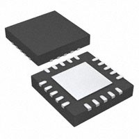
RGW PACKAGE
QFN-20
(TOP VIEW)
15
V+
14
NC
13
DRV
12
NC
11
V-
PIN ASSIGNMENTS
10
PIN NO.
NAME
1
M2
Mode Input
FUNCTION
2
M1
Mode Input
3
VIN
Noninverting Signal Input
4
SET
Input for Gain Setting; Inverting Input
5
IMON
Current Monitor Output
6
IAOUT
Instrumentation Amplifier Signal Output
7
IAIN–
Instrumentation Amplifier Inverting Input
8
IAIN+
Instrumentation Amplifier Noninverting Input
9
RG1
Instrumentation Amplifier Gain Resistor
10
RG2
Instrumentation Amplifier Gain Resistor
11
V–
Negative Power Supply
12
NC
No Internal Connection
13
DRV
14
NC
No Internal Connection
15
V+
Positive Power Supply
16
DGND
Ground for Digital I/O
17
EFCM
Error Flag for Common-Mode Over-Range, Active Low
18
EFLD
Error Flag for Load Error, Active Low
19
EFOT
Error Flag for Over Temperature, Active Low
20
OD
Pad
Exposed Pad
Operational Amplifier Output
Output Disable, Disabled Low
Exposed thermal pad must be connected to V−
Copyright © 2005–2011, Texas Instruments Incorporated
�XTR300
SBOS336C – JUNE 2005 – REVISED JUNE 2011
www.ti.com
TYPICAL CHARACTERISTICS
At TA = +25°C and V+ = ±20V, unless otherwise noted.
QUIESCENT CURRENT vs TEMPERATURE
QUIESCENT CURRENT vs SUPPLY VOLTAGE
1.90
3.0
1.88
2.5
1.86
1.84
IQ (mA)
IQ (mA)
2.0
1.5
1.0
1.82
1.80
1.78
1.76
1.74
0.5
1.72
0
-50
1.70
0
-25
25
50
75
100
10
125
15
20
25
Figure 5.
40
45
OPA OUTPUT SWING TO RAIL vs TEMPERATURE
0
2.2
IDRV = +24mA
IDRV = -24mA
-5
½VS - VOUT½ (V)
2.0
-10
-15
-20
IDRV = +20mA
1.8
1.6
IDRV = +10mA
1.4
IDRV = -20mA
-25
IDRV = -10mA
1.2
-30
1.0
-50
0
-25
25
50
75
100
125
-50
-25
0
Temperature (°C)
25
OPA GAIN AND PHASE vs FREQUENCY
-20
140
-40
-120
-140
Gain
-160
20
10
100
1k
10k 100k 1M
Frequency (Hz)
Figure 9.
Copyright © 2005–2011, Texas Instruments Incorporated
-200
10M
-135
RIA = 10kW
0
-180
RIA = 5kW
-20
-225
RIA = 1kW
Gain
Phase
-180
0
-90
RIA = 50kW
-40
1
10
100
1k
10k
100k
Phase (°)
-100
60
-45
RIA = 500kW
40
Phase (°)
80
40
60
-60
-80
0
RGAIN = 10kW
Gain (dB)
Phase
100
1
125
IA GAIN AND PHASE vs FREQUENCY
160
-20
0.001 0.01 0.1
100
80
0
20
75
Figure 8.
180
120
50
Temperature (°C)
Figure 7.
Gain (dB)
35
Figure 6.
INPUT BIAS CURRENT vs TEMPERATURE
(VIN, SET, IAIN+, IAIN−, RG1, RG2)
IB (nA)
30
Total Supply Voltage (V)
Temperature (°C)
1M
-270
10M
Frequency (Hz)
Figure 10.
11
�XTR300
SBOS336C – JUNE 2005 – REVISED JUNE 2011
www.ti.com
TYPICAL CHARACTERISTICS (continued)
At TA = +25°C and V+ = ±20V, unless otherwise noted.
IA CMRR AND PSRR vs FREQUENCY
140
140
120
120
CMRR, PSRR (dB)
100
PSRR80
60
PSRR+
40
CMRR
40
0
10
100
1k
10k
1
100k
10
100
1k
10k
Frequency (Hz)
Frequency (Hz)
Figure 11.
Figure 12.
SMALL−SIGNAL STEP RESPONSE
CURRENT MODE
LARGE−SIGNAL STEP RESPONSE
CURRENT MODE
IOUT = ±200mA
G=8
CL = 100nF || RL = 800W
CC = 4.7nF
RSET = 1kW
RGAIN = 10kW
See Figure 3
10V/div
1
100mV/div
PSRR60
20
0
50mV/div
PSRR+
80
CMRR
20
12
100
200ms/div
Figure 13.
Figure 14.
SMALL−SIGNAL STEP RESPONSE
VOLTAGE MODE
LARGE−SIGNAL STEP RESPONSE
VOLTAGE MODE
G=5
CL = 100nF || RL = 800W
CC = 4.7nF
RSET = 1kW
RGAIN = 10kW
See Figure 2
100k
IOUT = ±20mA
G=8
CL = 100nF || RL = 800W
CC = 4.7nF
RSET = 1kW
RGAIN = 10kW
See Figure 3
200ms/div
5V/div
CMRR, PSRR (dB)
OPA CMRR AND PSRR vs FREQUENCY
160
G=5
CL = 100nF || RL = 800W
CC = 4.7nF
RSET = 1kW
RGAIN = 10kW
See Figure 2
200ms/div
200ms/div
Figure 15.
Figure 16.
Copyright © 2005–2011, Texas Instruments Incorporated
�XTR300
SBOS336C – JUNE 2005 – REVISED JUNE 2011
www.ti.com
TYPICAL CHARACTERISTICS (continued)
At TA = +25°C and V+ = ±20V, unless otherwise noted.
INPUT−REFERRED NOISE SPECTRUM
VOLTAGE OUTPUT MODE
INPUT−REFERRED 0.1Hz to 10Hz NOISE
VOLTAGE OUTPUT MODE
1M
G=5
10k
1mV/div
Noise (nV/ÖHz)
100k
1k
100
10
1
1
10
100
1k
10k
1s/div
100k
Frequency (Hz)
Figure 17.
Figure 18.
INPUT−REFERRED NOISE SPECTRUM
CURRENT OUTPUT MODE
INPUT−REFERRED 0.1Hz to 10Hz NOISE
CURRENT OUTPUT MODE
1M
10k
1mV/div
Input- Referred Noise (nV/ÖHz)
G = 10
100k
1k
100
10
1
1
10
100
1k
10k
1s/div
100k
Frequency (Hz)
Figure 19.
Figure 20.
IA INPUT−REFERRED NOISE SPECTRUM
IA INPUT−REFERRED 0.1Hz to 10Hz NOISE
1M
100k
10k
1mV/div
Input-Referred Noise (nV/ÖHz)
G = 20
1k
100
10
1
1
10
100
1k
10k
100k
1s/div
Frequency (Hz)
Figure 21.
Copyright © 2005–2011, Texas Instruments Incorporated
Figure 22.
13
�XTR300
SBOS336C – JUNE 2005 – REVISED JUNE 2011
www.ti.com
TYPICAL CHARACTERISTICS (continued)
At TA = +25°C and V+ = ±20V, unless otherwise noted.
OPA OFFSET VOLTAGE DISTRIBUTION
IA OFFSET VOLTAGE DISTRIBUTION
18
30
Percent of Population (%)
14
12
10
8
6
4
2
0
25
20
15
10
5
Offset Voltage (mV)
OPA OFFSET VOLTAGE DRIFT DISTRIBUTION
3.0
2.4
1.8
IA OFFSET VOLTAGE DRIFT DISTRIBUTION
40
35
50
Percent of Population (%)
40
30
20
10
30
25
20
15
10
5
0
Offset Voltage Drift (mV/°C)
10
8
6
4
2
0
-2
-4
-6
-10
10
8
6
4
2
0
-2
-4
-6
-10
-8
0
-8
Offset Voltage Drift (mV/°C)
Figure 25.
Figure 26.
VOLTAGE MODE GAIN ERROR DISTRIBUTION
CURRENT MODE GAIN ERROR DISTRIBUTION
30
40
Percent of Population (%)
35
30
25
20
15
10
5
25
20
15
10
5
Figure 27.
1000
800
600
400
200
0
-400
-600
-800
1000
800
600
400
200
0
-200
-400
-600
-800
-1000
Gain Error (ppm)
-1000
0
0
-200
Percent of Population (%)
1.2
Figure 24.
60
Percent of Population (%)
0.6
Offset Voltage (mV)
Figure 23.
14
0
-0.6
-1.2
-1.8
-3.0
2.0
1.6
1.2
0.8
0.4
0
-0.4
-0.8
-1.2
-1.6
-2.0
0
-2.4
Percent of Population (%)
16
Gain Error (ppm)
Figure 28.
Copyright © 2005–2011, Texas Instruments Incorporated
�XTR300
SBOS336C – JUNE 2005 – REVISED JUNE 2011
www.ti.com
TYPICAL CHARACTERISTICS (continued)
At TA = +25°C and V+ = ±20V, unless otherwise noted.
CURRENT MODE NONLINEARITY DISTRIBUTION
60
50
50
Percent of Population (%)
40
30
20
10
40
30
20
10
Figure 29.
1000
800
600
400
Figure 30.
VOLTAGE MODE GAIN ERROR DRIFT DISTRIBUTION
CURRENT MODE GAIN ERROR DRIFT DISTRIBUTION
70
60
10
8
6
4
-10
1.0
0.8
0.6
0.4
0.2
0
-0.2
-0.4
0
-0.6
0
-0.8
10
-1.0
10
2
20
0
20
30
-2
30
40
-4
40
50
-6
50
-8
Percent of Population (%)
60
Gain Error Drift (ppm/°C)
Gain Error Drift (ppm/°C)
Figure 31.
Figure 32.
VOLTAGE MODE NONLINEARITY DRIFT DISTRIBUTION
CURRENT MODE NONLINEARITY DRIFT DISTRIBUTION
100
70
90
Percent of Population (%)
80
60
50
40
30
20
10
80
70
60
50
40
30
20
10
0
Nonlinearity Drift (ppm/°C)
Figure 33.
Copyright © 2005–2011, Texas Instruments Incorporated
10
8
6
4
2
0
-2
-6
-8
-10
1.0
0.8
0.6
0.4
0.2
0
-0.2
-0.4
-0.6
-0.8
-1.0
0
-4
Percent of Population (%)
200
Nonlinearity (ppm)
Nonlinearity (ppm)
Percent of Population (%)
0
-200
-400
-1000
1000
800
600
400
200
0
-200
-400
-600
-800
-1000
-600
0
0
-800
Percent of Population (%)
VOLTAGE MODE NONLINEARITY DISTRIBUTION
60
Nonlinearity Drift (ppm/°C)
Figure 34.
15
�XTR300
SBOS336C – JUNE 2005 – REVISED JUNE 2011
www.ti.com
TYPICAL CHARACTERISTICS (continued)
At TA = +25°C and V+ = ±20V, unless otherwise noted.
POSITIVE CURRENT LIMIT vs TEMPERATURE
NEGATIVE CURRENT LIMIT vs TEMPERATURE
36
-16
34
-18
32
30
-22
ILIMIT (mA)
ILIMIT (mA)
Voltage Mode
-20
Current Mode
28
26
24
Voltage Mode
22
-24
-26
-28
-30
20
-32
18
-34
16
Current Mode
-36
-50
0
-25
25
50
75
100
125
-50
-25
Temperature (°C)
75
100
Figure 35.
Figure 36.
NONLINEARITY vs OUTPUT CURRENT
(±24mA End Point Calibration)
NONLINEARITY vs OUTPUT CURRENT
(±20mA End Point Calibration)
0.025
+25°C
125
-55°C
+25°C
-55°C
0
Nonlinearity (%)
0
Nonlinearity (%)
50
Temperature (°C)
0.025
-0.025
25
0
+85°C
-0.050
-0.025
+125°C
+85°C
-0.050
-0.075
-0.075
+125°C
-0.100
-24 -20 -16 -12 -8
-4
0
4
8
Output Current (mA)
Figure 37.
16
12
16
20
24
-0.100
-24 -20 -16 -12 -8
-4
0
4
8
12
16
20
24
Output Current (mA)
Figure 38.
Copyright © 2005–2011, Texas Instruments Incorporated
�XTR300
SBOS336C – JUNE 2005 – REVISED JUNE 2011
www.ti.com
APPLICATION INFORMATION
V-
V+
GND
C2
100nF
C3
100nF
CC
47nF
GND1
XTR300
ICOPY
R3
1kW
IDRV
VIN
SIN
ROS
2kW
OPA
RC
15W
DRV
GND1
IAIN+
RSET
2kW
IIA
SG
RGAIN
10kW
IA
IAO
RG2
M2
RLOAD
R7
2.2kW
GND2
EFCM
OD
M1
C5
10nF
IAIN-
IAOUT
RIA
1kW
R6
2.2kW
CLOAD
RG1
GND1
External Load
C4
100nF
SET
OS
RIMON
1kW
Thermal
Pad (2)
Current Copy
IMON
IMON
V-
V+
Digital
Control
Error
Flags
EFLD
DGND
GND3
Logic Supply
(+2.7V to +5V)
EFOT
(1)
GND4
Pull-up Resistors
(10kW)
(1)
See the Electrical Characteristics and Digital Input and Output section for operating limits of DGND.
(2)
Connect thermal pad to V−.
Figure 39. Standard Circuit Configuration
The following information should be considered during XTR300 circuit configuration:
space
• RC ensures stability for unknown load conditions
• Recommended bypassing: 100nF or more for
and limits the current into the internal protection
supply bypassing at each supply.
diodes. C4 helps protect the device. Over-voltage
• RIMON can be in the kΩ-range or short-circuited if
clamp diodes (standard 1N4002) might be
not used. Do not leave this current output
necessary to protect the output.
unconnected—it would saturate the internal
• R6, R7, and C5 protect the IA.
current source. The current at this IMON output is
• RLOAD and CLOAD represent the load resistance
IDRV/10. Therefore, VIMON = RIMON (IDRV/10).
and load capacitance.
• R3 is not required but can match RSET (or
• RSET defines the transfer gain. It can be split to
RSET||ROS) to compensate for the bias current.
allow a signal offset and, therefore, allow a 5V
• RIA can be short-circuited if not used. Do not leave
single-supply digital-to-analog converter (DAC) to
this current output unconnected. RGAIN is selected
control a ±10V or ±20mA output signal.
to 10kΩ to match the output of 10V with 20mA for
the equal input signal.
space
space
space
Copyright © 2005–2011, Texas Instruments Incorporated
17
�XTR300
SBOS336C – JUNE 2005 – REVISED JUNE 2011
www.ti.com
The XTR300 can be used with asymmetric supply voltages; however, the minimum negative supply voltage
should be equal to or more negative than −3V (typically −5V). This supply value ensures proper control of 0V and
0mA with wire resistance, ground offsets, and noise added to the output. For positive output signals, the current
requirement from this negative voltage source is less than 5mA.
GND1 through GND4 must be selected to fulfill specified operating ranges. DGND must be in the range of (V−) ≤
DGND ≤ (V+) −7V.
Built on a robust high-voltage BiCMOS process, the XTR300 is designed to interface the 5V or 3V supply domain
used for processors, signal converters, and amplifiers to the high-voltage and high-current industrial signal
environment. It is specified for up to ±20V supply, but can also be powered asymmetrically (for example, +24V
and −5V). It is designed to allow insertion of external circuit protection elements and drive large capacitive loads.
FUNCTIONAL FEATURES
The XTR300 provides two basic functional blocks: an instrumentation amplifier (IA) and a driver that is a unique
operational amplifier (OPA) for current or voltage output. This combination represents an analog output stage
which can be digitally configured to provide either current or voltage output to the same terminal pin.
Alternatively, it can be configured for independent measurement channels.
Three open collector error signals are provided to indicate output related errors such as over-current or
open-load (EFLD) or exceeding the common-mode input range at the IA inputs (EFCM). An over-temperature flag
(EFOT) can be used to control output disable to protect the circuit. The monitor outputs (IMON and IAOUT) and the
error flags offer optimal testability during operation and configuration. The IMON output represents the current
flowing into the load in voltage output mode, while the IAOUT represents the voltage across the connectors in
current output mode. Both monitor outputs can be connected together when used in current or voltage output
mode because the monitor signals are multiplexed accordingly.
VOLTAGE OUTPUT MODE
In voltage output mode (M1 and M2 are connected low or left unconnected), the feedback loop through the IA
provides high impedance remote sensing of the voltage at the destination, compensating the resistance of a
protection circuit, switches, wiring, and connector resistance. The output of the IA is a current that is proportional
to the input voltage. This current is internally routed to the OPA summing junction through a multiplexer, as
shown in Figure 40.
A 1:10 copy of the output current of the OPA can be monitored at the IMON pin. This output current and the
known output voltage can be used to calculate the load resistance or load power.
During an output short-circuit or an over-current condition the XTR300 output current is limited and EFLD (load
error, active low) flag is activated.
18
Copyright © 2005–2011, Texas Instruments Incorporated
�XTR300
SBOS336C – JUNE 2005 – REVISED JUNE 2011
www.ti.com
CC
XTR300
Current Copy
IMON
ICOPY
RIMON
GND3
Input Signal
V-
V+
IDRV
VIN
OPA
SET
DRV
IAIN+
RSET
IIA
RG1
IA
RG2
GND1
EFCM
OD
L
M1
M2
Load
IAIN-
IAOUT
L
RGAIN
Digital
Control
Error
Flags
EFLD
GND2
EFOT
DGND
Figure 40. Simplified Voltage Output Mode Configuration
Applications not requiring the remote sense feature can use the OPA in stand-alone operation (M1 = high). In
this case, the IA is available as a separate input channel.
The IA gain can be set by two resistors, RGAIN and RSET:
R
VOUT = GAIN VIN
2RSET
(1)
or when adding an offset, VREF, to get bidirectional output with a single-ended input:
VIN
V - VREF
R
+ IN
VOUT = GAIN
RSET
ROS
2
(2)
(
(
The RSET resistor is also used in current output mode. Therefore, it is useful to define RSET for the current mode,
then set the ratio between current and voltage span with RGAIN.
Copyright © 2005–2011, Texas Instruments Incorporated
19
�XTR300
SBOS336C – JUNE 2005 – REVISED JUNE 2011
www.ti.com
CURRENT OUTPUT MODE
The XTR300 does not require a shunt resistor for current control because it uses a precise current mirror
arrangement.
In current output mode (M1 connected low, or left unconnected and M2 connected high) a precise copy of 1/10th
of the output is internally routed back to the summing junction of the OPA through a multiplexer, closing the
control loop for the output current.
The OPA driver can deliver more than ±24mA within a wide output voltage range. An open-output condition or
high-impedance load that prevents the flow of the required current activates the EFLD flag and the IA can become
overloaded and draw greater than 7mA saturation current.
While in current output mode, a current (IIA) that is proportional to the voltage at the IA input is routed to IAOUT
and can be used to monitor the load voltage. A resistor converts this current into voltage. This arrangement
makes level shifting easy.
Alternatively, the IA can be used as an independent monitoring channel. If this output is not used, connect it to
GND to maintain proper function of the monitor stage, as shown in Figure 41.
XTR300
V-
V+
Current Copy
IMON
ICOPY
IDRV
Input Signal
VIN
OPA
SET
DRV
IAIN+
RSET
IIA
RG1
IA
RG2
GND1
H
GND3
GND2
EFCM
OD
L
M1
M2
Load
IAIN-
IAOUT
RIA
RGAIN
Digital
Control
Error
Flags
EFLD
EFOT
DGND
Figure 41. Simplified Current Output Mode Configuration
The transconductance (gain) can be set by the resistor, RSET, according to the equation:
IOUT = 10 VIN
RSET
(3)
space
or when adding an offset VREF to get bidirectional output with a single-ended input:
VIN
V - VREF
+ IN
IOUT = 10
RSET
ROS
(
20
(
(4)
Copyright © 2005–2011, Texas Instruments Incorporated
�XTR300
SBOS336C – JUNE 2005 – REVISED JUNE 2011
www.ti.com
INPUT SIGNAL CONNECTION
It is possible to drive the XTR300 with a unidirectional input signal and still get a bidirectional output by adding an
additional resistor, ROS, and an offset voltage signal, VREF. It can be a mid-point voltage or a signal to shift the
output voltage to a desired value.
This design is illustrated in Figure 42a, Figure 42b, and Figure 42c. As with a normal operational amplifier, there
are several options for offset-shift circuits. The input can be connected for inverting or noninverting gain. Unlike
many op amp input circuits, however, this configuration uses current feedback, which removes the voltage
relationship between the noninverting input and output potential because there is no feedback resistor.
a) Noninverting Input
XTR300
VIN
(0 to VOFFSET)
OPA
VREF
ROS
2kW
RSET
2kW
IFeedback
b) Noninverting Input
XTR300
VIN
( VMIDSCALE)
OPA
VMIDSCALE
RSET
1kW
IFeedback
c) Inverting Input (VREF = VOFFSET)
XTR300
VOFFSET
VIN
(±VOFFSET)
OPA
RSET
1kW
IFeedback
Figure 42. Circuit Options for Op Amp Output Level-Shifting
The input bias current effect on the offset voltage can be reduced by connecting a resistor in series with the
positive input that matches the approximate resistance at the negative input. This resistor placed close to the
input pin acts as a damping element and makes the design less sensitive to RF noise. See R3 in Figure 39.
Copyright © 2005–2011, Texas Instruments Incorporated
21
�XTR300
SBOS336C – JUNE 2005 – REVISED JUNE 2011
www.ti.com
EXTERNALLY-CONFIGURED MODE: OPA AND IA
It is possible to use the precision of the operational amplifier (OPA) and instrumentation amplifier (IA)
independently from each other by configuring the digital control pins (M1 high). In this mode, the IA output
current is routed to IAOUT and the copy of the OPA output current is routed to IMON, as shown in Figure 4.
This mode allows external configuration of the analog signal routing and feedback loop.
The current output IA has high input impedance, low offset voltage and drift, and very high common-mode
rejection ratio. An external resistor (RIA) can be used to convert the output current of the IA (IIA) to an output
voltage. The gain is given by:
IIA = 2 VIN or VIA = 2RIA VIN
RGAIN
RGAIN
(5)
The OPA provides low drift and high voltage output swing that can be used like a common operational amplifier
by connecting a feedback network around it. In this mode, the copy of the output current is available at the IMON
pin (it includes the current into the feedback network). It provides an output current limit for protection, which can
be set between two ranges by M2. The error flag indicates an overcurrent condition, as well as indicating driving
the output into the supply rails.
Alternatively, the feedback can be closed through the IMON pin to create a precise voltage-to-current converter.
DRIVER OUTPUT DISABLE
The OPA output (DRV) can be switched to a high-impedance mode by driving the OD control pin low. This input
can be connected to the over-temperature flag, EFOT, and a pull-up resistor to protect the IC from
over-temperature by disconnecting the load.
The output disable mode can be used to sense and measure the voltage at the IA input pins without loading from
the DRV output. This mode allows testing of any voltage present at the I/O connector. However, consider the
bias current of the IA input pins.
The digital control inputs, M1 and M2, set the four operation modes of the XTR300 as shown in Table 1. When
M1 is asserted low, M2 determines voltage or current mode and the corresponding appropriate current limit (ISC)
setting. When M1 is high, the internal feedback connections are opened; IAOUT and IMON are both connected to
the output pins; and M2 only determines the current limit (ISC) setting.
M1 and M2 are pulled low internally with 1μA. Terminate these two pins to avoid noise coupling. Output disable
(OD) is internally pulled high with approximately 1μA. When connecting OD to EFOT, a 2.2kΩ pull-up resistor is
recommended.
Table 1. Summary of Configuration Modes (1)
(1)
22
M1
M2
MODE
L
L
VOUT
Voltage Output Mode, ISC = 20mA
DESCRIPTION
L
H
IOUT
Current Output Mode, ISC = 32mA
H
L
Ext
IA and IMON on ext. pins, ISC = 20A
H
H
Ext
IA and IMON on ext. pins, ISC = 32mA
OD is a control pin independent of M1 or M2.
Copyright © 2005–2011, Texas Instruments Incorporated
�XTR300
www.ti.com
SBOS336C – JUNE 2005 – REVISED JUNE 2011
DRIVING CAPACITIVE LOADS AND LOOP COMPENSATION
For normal operation, the driver OPA and the IA are connected in a closed loop for voltage output. In current
output mode, the current copy closes the loop directly.
In current output mode, loop compensation is not critical, even for large capacitive loads. However, in voltage
output mode, the capacitive load, together with the source impedance and the impedance of the protection
circuit, generates additional phase lag. The IA input might also be protected by a low-pass filter that influences
phase in the closed loop.
The loop compensation low-pass filter consists of CC and the parallel resistance of ROS and RSET. For loop
stability with large capacitive load, the external phase shift has to be added to the OPA phase. With CC, the
voltage gain of the OPA has to approach zero at the frequency where the total phase approaches 180° + 135°.
The best stability for large capacitive loads is provided by adding a small resistor, RC (15Ω). See the Output
Protection section.
An empirical method of evaluation is using a square wave input signal and observing the settling after transients.
Use small signal amplitudes only—steep signal edges cause excessive current to flow into the capacitive load
and may activate the current limit, which hides or prevents oscillation. A small-signal oscillation can be hidden
from large capacitive loads, but observing the IMON output on an appropriate resistor (use a similar value like
RSET||ROS) would indicate stability issues. Note that noise pulses at IMON during overload (EFLD active) are normal
and are caused by cycling of the current mirror.
The voltage output mode includes the IA in the loop. An additional low-pass filter in the input reverses the phase
and therefore increases the signal bandwidth of the loop, but also increases the delay. Again, loop stability has to
be observed. Overloading the IA disconnects the closed loop and the output voltage rails.
INTERNAL CURRENT SOURCES, SWITCHING NOISE, AND SETTLING TIME
The accuracy of the current output mode and the dc performance of the IA rely on dynamically-matched current
mirrors.
Identical current sources are rotated to average out mismatch errors. It can take several clock cycles of the
internal 100kHz oscillator (or a submultiple of that frequency) to reach full accuracy. This may dominate the
settling time to the 0.1% accuracy level and can be as much as 100μs in current output mode or 40μs in voltage
output mode.
A small portion of the switching glitches appear at the DRV output, and also at the IMON and IAMON outputs. The
standard circuit configuration, with RC, C4, and CC, which are required for loop compensation and output
protection, also helps reduce the noise to negligible levels at the signal output. If necessary, the monitor outputs
can be filtered with a shunt capacitor.
Copyright © 2005–2011, Texas Instruments Incorporated
23
�XTR300
SBOS336C – JUNE 2005 – REVISED JUNE 2011
www.ti.com
IA STRUCTURE, VOLTAGE MONITOR
The instrumentation amplifier has high-impedance NPN transistor inputs that do not load the output signal, which
is especially important in current output mode. The output signal is a controlled current that is multiplexed either
to the SET pin (to close the voltage output loop) or to IAOUT (for external access).
The principal circuit is shown in Figure 43. The two input buffer amplifiers reproduce the input difference voltage
across RGAIN. The resulting current through this resistor is bidirectionally mirrored to the output. That mirroring
results in the ideal transfer function of:
(IAIN+ – IAIN-)
IIA = IAOUT = 2
RGAIN
(6)
The accuracy and drift of RGAIN defines the accuracy of the voltage to current conversion. The high accuracy and
stability of the current mirrors result from a cycling chopper technique.
Current Mirror
IR
IR
IAIN+
A1
Current Mirror
IR
RGAIN
IR
Current Mirror
2IR
2IR
IIA
A2
IAIN-
2IR
2IR
Current Mirror
Figure 43. IA Block Diagram
The output current, IAOUT, of the instrumentation amplifier is limited to protect the internal circuitry. This current
limit has two settings controlled by the state of M2 (see Electrical Characteristics, Short-Circuit Current
specification). Note that if RSET is too small, the current output limitation of the instrumentation amplifier can
disrupt the closed loop of the XTR300 in voltage output mode. With M2 = low, the nominal RGAIN of 10kΩ allows
an input voltage of 20VPP, which produces an output current of 4mAPP. When using lower resistors for RGAIN that
can allow higher currents, the IA output current limitation must be taken into account.
CURRENT MONITOR
In current output mode (M2 = high), the XTR300 provides high output impedance. A precision current mirror
generates an exact 1/10th copy of the output current and this current is either routed to the summing junction of
the OPA to close the feedback loop (in the current output mode) or to the IMON pin for output current monitoring in
other operating modes.
The high accuracy and stability of this current split results from a cycling chopper technique. This design
eliminates the need for a precise shunt resistor or a precise shunt voltage measurement, which would require
high common-mode rejection performance.
During a saturation condition of the DRV output (the error flag is active), the monitor output (IMON) shows a
current peak because the loop opens. Glitches from the current mirror chopper appear during this time in the
monitor signal. This part of the signal cannot be used for measurement.
24
Copyright © 2005–2011, Texas Instruments Incorporated
�XTR300
SBOS336C – JUNE 2005 – REVISED JUNE 2011
www.ti.com
ERROR FLAGS
The XTR300 is designed for testability of its proper function and allows observation of the conditions at the load
connection without disrupting service.
If the output signal is not in accordance to the transfer function, an error flag is activated (limited by the dynamic
response capabilities). These error flags are in addition to the monitor outputs, IMON and IAOUT, which allow the
momentary output current (in voltage mode) or output voltage (in current mode) to be read back.
This combination of error flag and monitor signal allows easy observation of the XTR300 for function and working
condition, providing the basis for not only remote control, but also for remote diagnosis.
All error flags of the XTR300 have open collector outputs with a weak pull-up of approximately 1μA to an internal
5V. External pull-up resistors to the logic voltage are required when driving 3V or 5V logic.
The output sink current should not exceed 5mA. This is just enough to directly drive optical-couplers, but a
current-limiting resistor is required.
There are three error flags:
• IA Common-Mode Over-Range (EFCM)—goes low as soon as the inputs of the IA reach the limits of the
linear operation for the input voltage. This flag shows noise from the saturated current mirrors which can be
filtered with a capacitor to GND.
• Load Error (EFLD)—indicates fault conditions driving voltage or current into the load. In voltage output mode
it monitors the voltage limits of the output swing and the current limit condition caused from short or low load
resistance. In current output mode it indicates a saturation into the supply rails from a high load resistance or
open load.
• Over-Temperature Flag (EFOT)—is a digital output that goes low if the chip temperature reaches a
temperature of +140°C and resets as soon as it cools down to +125°C. It does not automatically shut down
the output; it allows the user system to take action on the situation. If desired, this output can be connected to
output disable (OD) which disables the output and therefore removes the source of power. This connection
acts like an automatic shut down, but requires a 2.2kΩ external pull-up resistor to safely override the internal
current sources. The IA channel is not affected, which allows continuous observation of the voltage at the
output.
DIGITAL I/O AND GROUND CONSIDERATIONS
The XTR300 offers voltage output mode, current output mode, external configuration, and instrumentation mode
(voltage input). In addition, the internal feedback mode can be disconnected and external loop connections can
be made. These modes are controlled by M1 and M2 (see the function table). The OD input pin controls enable
or disable of the output stage (OD is active low).
The digital I/O is referenced to DGND and signals on this pin should remain within 5V of the DGND potential.
This DGND pin carries the output low-current (sink current) of the logic outputs. DGND can be connected to a
potential within the supply voltage but needs to be 8V below the positive supply. Proper connection avoids
current from the digital outputs flowing into the analog ground.
CAUTION
It is important to note that DGND has normally reverse-biased diodes connected to the
supply. Therefore, high and destructive currents could flow if DGND is driven beyond
the supply rails by more than a diode forward voltage. Avoid this condition during
power-on and power-off!
Copyright © 2005–2011, Texas Instruments Incorporated
25
�XTR300
SBOS336C – JUNE 2005 – REVISED JUNE 2011
www.ti.com
OUTPUT PROTECTION
The XTR300 is intended to operate in a harsh industrial environment. Therefore, a robust semiconductor process
was chosen for this design. However, some external protection is still required.
The instrumentation amplifier inputs can be protected by external resistors that limit current into the protection
cell behind the IC-pins, as shown in Figure 44. This cell conducts to the power-supply connection through a
diode as soon as the input voltage exceeds the supply voltage. The circuit configuration example shows how to
arrange these two external resistors.
The bias current is best cancelled if both resistors are equal. The additional capacitor reduces RF noise in the
input signal to the IA.
R6
2.2kW
IAIN+
VSENSE+
RG1
IA
RG2
C5
10nF
RGAIN
R7
2.2kW
VSENSE-
IAIN-
Figure 44. Current-Limiting Resistors
The load connection to the DRV output must be low impedance; therefore, external protection diodes may be
necessary to handle excessive currents, as shown in Figure 45. The internal protection diodes start to conduct
earlier than a normal external PN-type diode because they are affected by the higher die temperature. Therefore,
either Schottky diodes are required, or an additional resistor (RC) can be placed in series with the input. An
example of this protection is shown in Figure 45. Assuming the standard diodes limit the voltage to 1.4V and the
internal diodes clamp at 0.7V, this resistor can limit the current into the internal protection diodes to 50mA:
(1.4V – 0.7V)
= 47mA
15W
(7)
RC is also part of the recommended loop compensation. C4 helps protect the output against RFI and high-voltage
spikes.
CC
47nF
V+
D
1N4002
XTR300
OPA
DRV
RC
15W
I/V OUT
D
1N4002
C4
100nF
V-
Figure 45. Example for DRV Output Protection
26
Copyright © 2005–2011, Texas Instruments Incorporated
�XTR300
SBOS336C – JUNE 2005 – REVISED JUNE 2011
www.ti.com
POWER ON/OFF GLITCH
When power is turned on or off, most analog amplifiers generate some glitching of the output because of internal
circuit thresholds and capacitive charges. Characteristics of the supply voltage, as well as its rise and fall time,
directly influence output glitches. Load resistance and capacitive load also affect the amplitude.
The output disable control (OD) cannot fully suppress glitches during power-on and power-off, but reduces the
energy significantly. The glitch consists of a small amount of current and capacitive charge (voltage) that reacts
with the resistive and capacitive load. The bias current of the IA inputs that are normally connected to the output
also generate a voltage across the load.
Figure 46 indicates no glitches when transitioning between disable and enable. This measurement is made with
a load resistance of 1kΩ and tested in the circuit configuration of Figure 39.
Output
0.5V/div
OD
2.0V/div
Time (10ms/div)
Figure 46. Output Signal During Toggle of OD
When power is off or with low supply, the output is diode clamped to the momentary supply voltage, but can float
while output disabled within those limits unless terminated. Only an external switch (relays or opto-relays) can
isolate the output under such conditions. Refer to Figure 47 for an illustration of this configuration. The same
consideration applies if low impedance zero output is required, even during power-off.
CC
47 nF
VEN_OPTO
0V to 5V
RLED
5k
XTR300
+
RC
15
DRV
OPA
–
CPC1017N
SOUT
4
1
C4
100 nF
+
IAIN+
RG1
IA
RG2
–
IAIN–
ILED
0mA to 1 mA
R6
2.2 k
RGAIN
10 k
C5
10 nF
R7
2.2 k
3
2
RLOAD
1k
Figure 47. Example for Opto-Relay Output Isolation
Copyright © 2005–2011, Texas Instruments Incorporated
27
�XTR300
SBOS336C – JUNE 2005 – REVISED JUNE 2011
www.ti.com
LAYOUT CONSIDERATIONS
Supply bypass capacitors should be close to the package and connected with low-impedance conductors. Avoid
noise coupled into RGAIN, and observe wiring resistance. For thermal management, see the Package and Heat
Sinking section.
Layout for the XTR300 is not critical; however, its internal current chopping works best with good (low dynamic
impedance) supply decoupling. Therefore, avoid throughhole contacts in the connection to the bypass capacitors
or use multiple through-hole contacts. Switching noise from chopper-type power supplies should be filtered
enough to reduce influence on the circuit. Small resistors (2Ω, for example) or damping inductors in series with
the supply connection (between the dc/dc converter and the XTR circuit) act as a decoupling filter together with
the bypass capacitor, as shown in Figure 48.
Resistors connected close to the input pins help dampen environmental noise coupled into conductor traces.
Therefore, place the OPA input- and IA input-related resistors close to the package. Also, avoid additional wire
resistance in series to RSET, ROS, and RGAIN (observe the reliability of the through-hole contacts), because this
resistance could produce gain and offset error as well as drift; 1Ω is already 0.1% of the 1kΩ resistor.
The exposed lead-frame die pad on the bottom of the package must be connected to V−, pin 11 (see the QFN
Package and Heat Sinking section for more details).
V-
V+
L1
10mH
L2
10mH
CB1
100nF
CB2
100nF
CB3
1mF
CB4
1mF
V+
V-
XTR300
Figure 48. Suggested Supply Decoupling for Noisy Chopper-Type Supplies
QFN PACKAGE AND HEAT SINKING
The XTR300 is available in a QFN package. This leadless, near-chip-scale package maximizes board space and
enhances thermal and electrical characteristics of the device through an exposed thermal pad.
Packages with an exposed thermal pad are specifically designed to provide excellent power dissipation, but
printed circuit board (PCB) layout greatly influences overall heat dissipation. The thermal resistance from
junction-to-ambient (θJA) is specified for the packages with the exposed thermal pad soldered to a normalized
PCB, as described in Technical Brief SLMA002, PowerPAD™ Thermally-Enhanced Package. See also
EIA/JEDEC Specifications JESD51-0 to 7, QFN/SON PCB Attachment (SLUA271), and Quad Flatpack No-Lead
Logic Packages (SCBA017). These documents are available for download at www.ti.com.
NOTE: All thermal models have an accuracy variation of ±20%.
Component population, layout of traces, layers, and air flow strongly influence heat dissipation. Worst-case load
conditions should be tested in the real environment to ensure proper thermal conditions. Minimize thermal stress
for proper long-term operation with a junction temperature well below +125°C.
The exposed lead-frame die pad on the bottom of the package must be connected to the V− pin.
28
Copyright © 2005–2011, Texas Instruments Incorporated
�XTR300
www.ti.com
SBOS336C – JUNE 2005 – REVISED JUNE 2011
POWER DISSIPATION
Power dissipation depends on power supply, signal, and load conditions. It is dominated by the power dissipation
of the output transistors of the OPA. For dc signals, power dissipation is equal to the product of output current,
IOUT and the output voltage across the conducting output transistor (VS – VOUT).
It is very important to note that the temperature protection does not shut the part down in overtemperature
conditions, unless the EFOT pin is connected to the output enable pin OD; see the Driver Output Disable section.
The power that can be safely dissipated in the package is related to the ambient temperature and the heatsink
design and conditions. The QFN package with an exposed thermal pad is specifically designed to provide
excellent power dissipation, but board layout greatly influences the heat dissipation.
To appropriately determine the required heatsink area, required power dissipation should be calculated and the
relationship between power dissipation and thermal resistance should be considered to minimize overheat
conditions and allow for reliable long-term operation.
The heat sinking efficiency can be tested using the EFOT output signal. This output goes low at nominally +140°C
junction temperature (assume 6% tolerance). With full power dissipation (for example, maximum current into a
0Ω load), the ambient temperature can be slowly raised until the OT flag goes low. This flag would indicate the
minimum heat-sinking for the usable operation condition.
The recommended landing pattern for the QFN package is shown at the end of this data sheet.
Copyright © 2005–2011, Texas Instruments Incorporated
29
�XTR300
SBOS336C – JUNE 2005 – REVISED JUNE 2011
www.ti.com
REVISION HISTORY
NOTE: Page numbers for previous revisions may differ from page numbers in the current version.
Changes from Revision B (March, 2006) to Revision C
Page
•
Updated document format to current standards ................................................................................................................... 1
•
Deleted information regarding HART digital communication throughout document ............................................................. 1
•
Added footnote regarding small-signal measurement with no capacitive load in Electrical Characteristics (Voltage
Output Mode) ........................................................................................................................................................................ 3
•
Corrected Nominal setup for ±20mA Output parameter from ±20V Output in Electrical Characteristics (Current
Output Mode) ........................................................................................................................................................................ 4
•
Changed Common-Mode Voltage Range parameter to Input Voltage Range in Electrical Characteristics
(Instrumentation Amplifier) .................................................................................................................................................... 6
•
Added conditions to Short Circuit Current parameter in Electrical Characteristics (Instrumentation Amplifier) ................... 6
•
Changed last paragraph of Driver Output Disable section ................................................................................................. 22
•
Corrected footnote to Table 1 ............................................................................................................................................. 22
•
Revised Over-Temperature Flag description in Error Flags section to indicate the need for a 2.2kΩ resistor .................. 25
•
Revised Power On/Off Glitch section and added Figure 47 ............................................................................................... 27
•
Updated and combined QFN Package and Heat Sinking sections .................................................................................... 28
•
Added Power Dissipation section ....................................................................................................................................... 29
30
Copyright © 2005–2011, Texas Instruments Incorporated
�PACKAGE OPTION ADDENDUM
www.ti.com
13-Aug-2021
PACKAGING INFORMATION
Orderable Device
Status
(1)
Package Type Package Pins Package
Drawing
Qty
Eco Plan
(2)
Lead finish/
Ball material
MSL Peak Temp
Op Temp (°C)
Device Marking
(3)
(4/5)
(6)
XTR300AIRGWR
ACTIVE
VQFN
RGW
20
3000
RoHS & Green
NIPDAU
Level-2-260C-1 YEAR
-55 to 125
XTR
300
XTR300AIRGWT
ACTIVE
VQFN
RGW
20
250
RoHS & Green
NIPDAU
Level-2-260C-1 YEAR
-55 to 125
XTR
300
XTR300AIRGWTG4
ACTIVE
VQFN
RGW
20
250
RoHS & Green
NIPDAU
Level-2-260C-1 YEAR
-55 to 125
XTR
300
(1)
The marketing status values are defined as follows:
ACTIVE: Product device recommended for new designs.
LIFEBUY: TI has announced that the device will be discontinued, and a lifetime-buy period is in effect.
NRND: Not recommended for new designs. Device is in production to support existing customers, but TI does not recommend using this part in a new design.
PREVIEW: Device has been announced but is not in production. Samples may or may not be available.
OBSOLETE: TI has discontinued the production of the device.
(2)
RoHS: TI defines "RoHS" to mean semiconductor products that are compliant with the current EU RoHS requirements for all 10 RoHS substances, including the requirement that RoHS substance
do not exceed 0.1% by weight in homogeneous materials. Where designed to be soldered at high temperatures, "RoHS" products are suitable for use in specified lead-free processes. TI may
reference these types of products as "Pb-Free".
RoHS Exempt: TI defines "RoHS Exempt" to mean products that contain lead but are compliant with EU RoHS pursuant to a specific EU RoHS exemption.
Green: TI defines "Green" to mean the content of Chlorine (Cl) and Bromine (Br) based flame retardants meet JS709B low halogen requirements of


 工商网监
湘ICP备2023018690号
工商网监
湘ICP备2023018690号
