CM1214A 1 and 2 Channel PicoGuardTM AC Signal ESD Protector
Features
• • • • • • • Single channel ESD protection for an AC signal up to ±5V for 0.25W transmit power Connects two channels in series for signals up to +10V (1W transmit power) ±8kV ESD protection per IEC 61000-4-2 contact discharge Sub-1pF loading capacitance Minimal variation with voltage and temperature Each I/O pin can withstand over 1000 ESD strikes* SOT23-3 and MSOP-8 lead-free packages
Product Description
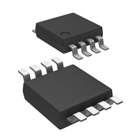
The CM1214A PicoGuard™ ESD protector is used to protect bipolar signal lines against electrostatic discharge (ESD). The CM1214A allows operation in high-speed environments with signals levels up to ±5V. The CM1214A comes in two versions: • The CM1214A-01SO is a single channel ESD protector and is available in a 3-lead SOT23-3 package. • The CM1214A-02MR is a dual channel ESD protector and is available in an 8-lead MSOP-8 package. The low sub-1pF loading capacitance makes the CM1214A-01SO ideal for protecting high-speed interfaces including RF switches and amplifiers. The CM1214A-02MR is ideal for dual high-speed signal pairs used in Gigabit Ethernet, ADSL, etc. The CM1214A-02MR can also be used for higher transmit voltage applications by connecting the two channels in series. Both devices come in lead-free finishing.
Applications
• • • • RF switch and amplifier protection RF modules and RF IC protection Wireless handsets and WLAN High-speed AC signals for Gbit Ethernet, etc.
Electrical Schematics
CH1 CH1 CH3
CH2
CM1214A-01SO
CH2
CH4
CM 1214A-02MR
*Standard test condition is IEC61000-4-2 level 4 test circuit with each pin subjected to ±8kV contact discharge for 1000 pulses. Discharges are timed at 1 second intervals and all 1000 strikes are completed in one continuous test run. The part is then subjected to standard production test to verify that all of the tested parameters are within spec after the 1000 strikes.
© 2007 California Micro Devices Corp. All rights reserved.
490 N. McCarthy Blvd., Milpitas, CA 95035-5112
●
Tel: 408.263.3214 Issue A – 10/29/07
●
Fax: 408.263.7846
●
www.cmd.com
1
�CM1214A
PACKAGE / PINOUT DIAGRAMS
Top View
CH1
1
Top View
CH1 N.C.* 1 8 N.C.* CH2 CH4 N.C.*
RF2S
2 3 4
7 6 5
RF1S
2
3
N.C.*
N.C.* CH3
CH2
SOT23-3
MSOP-8
Notes: 1) These drawings are not to scale. 2) All N.C. pins must be left floating (i.e., not connected to the PCB). See applications section for more information.
SOT23-3 PACKAGE PIN DESCRIPTIONS PIN 1 2 3 NAME DESCRIPTION CH1 CH2 N.C. ESD Channel ESD Channel No connect PIN 1 2 3 4 5 6 7 8
MSOP-8 PACKAGE PIN DESCRIPTIONS NAME DESCRIPTION CH1 N.C. N.C. CH3 N.C. CH4 CH2 N.C. ESD Channel No connect No connect ESD Channel No connect ESD Channel ESD Channel No connect
Ordering Information
PART NUMBERING INFORMATION
Lead-free Finish Pins 3 8 Package SOT23 MSOP Ordering Part Number1 CM1214A-01SO CM1214A-02MR Part Marking RF1S RF2S
Note 1: Parts are shipped in Tape & Reel form unless otherwise specified.
© 2007 California Micro Devices Corp. All rights reserved.
2
490 N. McCarthy Blvd., Milpitas, CA 95035-5112
●
Tel: 408.263.3214 Issue A – 10/29/07
●
Fax: 408.263.7846
●
www.cmd.com
�CM1214A
Specifications
ABSOLUTE MAXIMUM RATINGS
PARAMETER DC Voltage between CH pins Operating Temperature Range Storage Temperature Range Package Power Rating SOT23-3 Package (CM1214A-01SO) MSOP8 Package (CM1214A-02MR) RATING 7 –40 to +85 –65 to +150 225 400 UNITS V °C °C mW mW
STANDARD OPERATING CONDITIONS
PARAMETER Operating Temperature Range RATING –40 to +85 UNITS °C
ELECTRICAL OPERATING CHARACTERISTICS (SEE NOTE 1)
SYMBOL PARAMETER VST VESD Standoff Voltage ESD Voltage Protection Peak discharge voltage between CH pins a) Contact discharge per IEC 61000-4-2 standard Channel Leakage Current Dynamic Resistance Channel Clamp Voltage Channel Input Capacitance Voltage between CH pins = 0V Voltage between CH pins = 5V
Note 1: Note 2: Note 3: Note 4: Note 5:
CONDITIONS I=10μA Notes 2, 3 and 4
MIN
TYP ±7
MAX
UNITS V
±8 TA=25°C, 5.5V between CH pins TA=25°C, IPP = 1A, tP = 8/20μS; Any I/O pin to Ground; Notes 2 and 5 TA=25°C, IPP = 1A, tP = 8/20μS; Notes 2 & 5 Measured at 1MHz between CH pins; Note 2 applies 0.4 0.35 ±0.1 1.36 11.3 ±1.0
kV μA Ω V
ILEAK RDYN VCL CIN
0.6 0.54
0.9 0.8
pF pF
All parameters specified at TA = –40°C to +85°C unless otherwise noted. These parameters guaranteed by design and characterization. Standard IEC 61000-4-2 with CDischarge = 150pF, RDischarge = 330Ω,. From CH pin with other CH pin grounded. No Connect pins are left open for all tests.
© 2007 California Micro Devices Corp. All rights reserved.
490 N. McCarthy Blvd., Milpitas, CA 95035-5112
●
Tel: 408.263.3214 Issue A – 10/29/07
●
Fax: 408.263.7846
●
www.cmd.com
3
�CM1214A
Performance Information
Typical Capacitance Characteristics vs. Voltage Figure 1 illustrates how the loading capacitance remains mainly flat across the voltage range from 0V to 5V, the voltage between CH pins. Typical Voltage-Current (VI) Characteristics (high current, pulse condition) Figure 3 shows how the CM1214A experiences a symmetrical I/V curve, without any snapback or trigger voltage. The curve shows only one polarity.
10 9 8 7 6 5 4 3 2
0 1 2 Voltage [V] 3 4 5
Capacitance vs. Voltage (measured at 1MHz)
1.2 1.1 1 0.9 0.8 0.7 0.6 0.5 0.4 0.3 0.2
Capacitance [pF]
Current [uA]
1 0 0 1 2 3 4 5 6 7 8
Figure 1. CM1214A Capacitance vs. Voltage Typical Voltage Current (VI) Characteristics (low current) Figure 2 shows how the CM1214A experiences a symmetrical I/V curve, without any snapback or trigger voltage. It gradually starts to turn on at about 6V and clamps about 7V.
10 9 8 7 6 4 3 2 1 0 0 1 2 3 4 5 6 7 8
Input Capacitance (pF)
Voltage [V]
Figure 3. CM1214A VI Characteristics, Low Current, Pulse (clamping) Condition
Typical Capacitance Temperature
Characteristics
vs.
Figure 4 illustrates the loading capacitance for both 0VDC and 1.65VDC input across the -40 to 85°C temperature range.
Current [uA]
0.660 0.640 0.620 0.600 0.580 0.560 0.540 0.520 -50 -25 0 25 50 Temperature (°C) 75 100
0V DC Input Bias 1.65V DC Input Bias
5
Voltage [V]
Figure 2. CM1214A VI Characteristics, Low Current
Figure 4. CM1214A Capacitance vs. Temperature
© 2007 California Micro Devices Corp. All rights reserved.
4
490 N. McCarthy Blvd., Milpitas, CA 95035-5112
●
Tel: 408.263.3214 Issue A – 10/29/07
●
Fax: 408.263.7846
●
www.cmd.com
�CM1214A
Performance Information (cont’d)
Typical Filter Performance (nominal conditions unless specified otherwise, 50 Ohm Environment)
Figure 5. Insertion Loss vs. Frequency (0V DC Bias)
Figure 6. Insertion Loss vs. Frequency (2.5V DC Bias)
© 2007 California Micro Devices Corp. All rights reserved.
490 N. McCarthy Blvd., Milpitas, CA 95035-5112
●
Tel: 408.263.3214 Issue A – 10/29/07
●
Fax: 408.263.7846
●
www.cmd.com
5
�CM1214A
Application Information
CM1214A-01SO The CM1214A-01SO protects a single bipolar signal line often found in RF circuits. One I/O pin (pin 1 for example) is connected to the signal line for protection, and the other I/O pin is tied to GND. It is important to have a solid ground connection to reduce the clamping voltage. Pin 3 of the 3-lead SOT23 must be left open (and not connected on the PCB). CM1214A-02MR The CM1214A-02MR protects two bipolar lines, such as for Gbit Ethernet. The PCB traces underneath the package connect across to the corresponding pins (Pins 1, 4, 6 and 7). Pins 2, 3, 5 and 8 of the MSOP-8 package must be left open (and not connected on the PCB). Any disturbance on the line above or below the standoff voltage is clamped.
RF ANTENNA
LNA
SIGNAL LINE SWITCH ESD N.C. ESD GND
SOT23-3
C
L
PA
Figure 7. Typical Application - RF Switch and Amplifier Protection, CM1214A-01SO in 3-lead SOT23
R CM1214A-02MR
R CM1214A-02MR
Figure 8. Typical Application - Ethernet Protection, CM1214A-02MR in 8-lead MSOP
© 2007 California Micro Devices Corp. All rights reserved.
6
490 N. McCarthy Blvd., Milpitas, CA 95035-5112
●
Tel: 408.263.3214 Issue A – 10/29/07
●
Fax: 408.263.7846
●
www.cmd.com
�CM1214A
Application Information (cont’d)
IEEE1394
1 2 3 4
PHY
LLC
GALV iso
CM1214-02 CM1214-02
GND
Keep the ESD devices on the PHY side of the galvanic isolation and inside the VCC domain of the PHY controller.
Figure 9. Typical Application - IEEE1394 Protection, CM1214A-02MR in 8-lead MSOP
© 2007 California Micro Devices Corp. All rights reserved.
490 N. McCarthy Blvd., Milpitas, CA 95035-5112
●
Tel: 408.263.3214 Issue A – 10/29/07
●
Fax: 408.263.7846
●
www.cmd.com
7
�CM1214A
Mechanical Details
The CM1214A is supplied in SOT23-3 and MSOP-8 packages. Dimensions are presented below. SOT23-3 Mechanical Specifications The CM1214A-01SO is supplied in a 3-pin SOT23 package. Dimensions are presented below.
TOP VIEW
Mechanical Package Diagrams
b
PACKAGE DIMENSIONS
Package Pins Dimensions A A1 b c D E E1 e e1 L L1 # per tape and reel Millimeters Min 0.89 0.01 0.30 0.08 2.80 2.10 1.20 Max 1.12 0.10 0.50 0.20 3.04 2.64 1.40 Min 0.0350 0.0004 0.0118 0.0031 0.1102 0.0827 0.0472 SOT23-3 (JEDEC name is TO-236) 3 Inches Max 0.0441 0.0039 0.0197 0.0079 0.1197 0.1039 0.0551 e
1
3
E1 E
2
e1
SIDE VIEW
D
A1 A
0.95 BSC 1.90 BSC 0.40 0.60 0.54 REF
0.0374 BSC 0.0748 BSC 0.0157 0.0236
END VIEW
0.0213 REF 3000 pieces
Controlling dimension: millimeters
c L1 L
Package Dimensions for SOT23-3
© 2007 California Micro Devices Corp. All rights reserved.
8
490 N. McCarthy Blvd., Milpitas, CA 95035-5112
●
Tel: 408.263.3214 Issue A – 10/29/07
●
Fax: 408.263.7846
●
www.cmd.com
�CM1214A
Mechanical Details (cont’d)
MSOP-8 Mechanical Specifications, 8 pin The CM1214A-02MR is supplied in an 8-pin MSOP package. Dimensions are presented below. Mechanical Package Diagrams
TOP VIEW
PACKAGE DIMENSIONS
8 7
D
6 5
Package Pins Dimensions A A1 B C D E e H L # per tape and reel Millimeters Min 0.75 0.05 0.28 0.13 2.90 2.90 Max 0.95 0.15 0.38 0.23 3.10 3.10
MSOP 8 Inches Min 0.030 0.002 0.011 0.005 0.114 0.114 Max 0.037 0.006 0.015 0.009 0.122 0.122
SIDE VIEW 1 2 3 4
H
Pin 1 Marking
E
0.65 BSC 4.90 BSC 0.40 0.70
0.026 BSC 0.193 BSC 0.016 0.028 4000 pieces
SEATING PLANE
A A1 B e
END VIEW
Controlling dimension: millimeters
C
L Package Dimensions for MSOP-8
© 2007 California Micro Devices Corp. All rights reserved.
490 N. McCarthy Blvd., Milpitas, CA 95035-5112
●
Tel: 408.263.3214 Issue A – 10/29/07
●
Fax: 408.263.7846
●
www.cmd.com
9
�