CAT3604
4-Channel Regulated Charge Pump White LED Driver
FEATURES
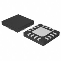
Drives individually up to 4 LEDs Output current up to 30mA per LED Digital control On/Off of each LED Compatible with supply voltage of 3V to 5.5V Power efficiency up to 93% 2 modes of operation 1x and 1.5x Automatic short circuit detect/disable High-frequency Operation at 1MHz Low value ceramic capacitors "604" compatible pinout Soft start and current limiting TQFN 16-pad package, 4 x 4mm, 0.8mm max height
DESCRIPTION
The CAT3604 is a charge pump operating in either 1x (LDO) mode or 1.5x fractional mode regulating current through each of the 4 LED pins. Operation at a fixed high frequency of 1MHz typical allows the use of very small value ceramic capacitors. The CAT3604 drives white light-emitting diodes (LEDs) connected in parallel and provides tightly matched regulated current to achieve uniformity of brightness in LCD backlighting applications. An external resistor RSET controls the output current level. LED currents of up to 30mA are supported over a range of input supply voltages from 3V to 5.5V, making the device ideal for battery-powered applications. LED dimming can be accomplished by several methods including using a DC voltage to set the RSET pin current, applying a PWM signal on the Control signals, or adding a switched resistor in parallel with RSET. The Enable input pin allows the device to be placed in power-down mode with "zero” quiescent current. The CAT3604 features short circuit and overcurrent limiting protection. The device is available in a 16-pad TQFN package with a max height of 0.8mm. For Ordering Information details, see page 11.
APPLICATION
Color LCD and keypad Backlighting Cellular Phones Handheld Devices Digital Cameras PDAs Portable MP3 players
ORDERING INFORMATION
Part Number Package
(2)
Quantity per Reel Marking 2000 2000 G364 CDBA
CAT3604HV4-T2 TQFN-16 (1) CAT3604HV4-GT2 TQFN-16
Notes: (1) Matte-Tin Plated Finish (RoHS-compliant). (2) NiPdAu Plated Finish (RoHS-compliant).
TYPICAL APPLICATION CIRCUIT
1µF 1µF
C1+ VIN Battery VIN 3V to 4.2V CIN 1µF EN Control 0 Control 1 Control 2 RSET 24kΩ EN CTR0 CTR1 CTR2 RSET
C1- C2+
C2VOUT
VOUT COUT 1µF 20mA
CAT3604 LED1 LED2 LED3 GND LED4
© Catalyst Semiconductor, Inc. Characteristics subject to change without notice
1
Doc. No. MD-5008 Rev. J
�CAT3604
PIN CONFIGURATION (1)
TQFN 16-pad (4 x 4mm) (Top View)
LED1
16 EN CTR0 CTR1 CTR2 1 2 3 4 5 6 7 8 GND
15
LED2 VOUT
14
LED3
13 12 GND 11 C2+ 10 C29 C1-
LED4
RSET
VIN
C1+
PIN DESCRIPTIONS
Pin Number 1 2 3 4 5 6 7 8 9 10 11 12 13 14 15 16 Pad Name EN CTR0 CTR1 CTR2 RSET VOUT VIN C1+ C1 C2 C2+ GND LED4 LED3 LED2 LED1 GND Pad Function Enable input, active HIGH Digital control input 0 Digital control input 1 Digital control input 2 The LED output current is set by the current sourced out of the RSET pin Charge pump output connected to the LED anodes Supply voltage Bucket capacitor 1 terminal Bucket capacitor 1 terminal Bucket capacitor 2 terminal Bucket capacitor 2 terminal Ground reference LED 4 cathode terminal LED 3 cathode terminal LED 2 cathode terminal LED 1 cathode terminal Ground reference
Notes: (1) The package exposed pad is electrically connected inside the package to GND and to pin 12.
Doc. No. MD-5008 Rev. J
2
© Catalyst Semiconductor, Inc. Characteristics subject to change without notice
�CAT3604
ABSOLUTE MAXIMUM RATINGS
Parameter VIN, VOUT, LEDx voltage EN, CTRx voltage RSET voltage RSET current Ambient Temperature Range Storage Temperature Range Lead Temperature ESD Ratings Human Body Model (HBM) Machine Model (MM) (1) Rating -0.3 to 7.0 -0.3 to VIN -0.3 to VIN ±1 -40 to +85 -65 to +160 300 2000 200 Unit V V V mA ºC ºC ºC V V
RECOMMENDED OPERATING CONDITIONS
Parameter VIN Ambient Temperature Range Input/Output/Bucket Capacitors ILED per LED pin Range 3.0 to 5.5 -40 to +85 1 ± 20% typical 0 to 30 Unit V ºC µF mA
Typical application circuit with external components is shown on page 1.
ELECTRICAL OPERATING CHARACTERISTICS
Limits over recommended operating conditions unless specified otherwise. Typical values at TA = 25˚C, VIN = 3.5V, IRSET = 5µA Symbol IQ VRSET ILED ILED-ACC ILED-DEV ROUT fOSC TDROPOUT IEN-CTR VEN-CTR ISC ILIM Parameter Quiescent Current RSET Regulated Voltage Programmed LED Current LED Current Accuracy LED Channel Matching Output Resistance (Open Loop) Charge Pump Frequency 1x to 1.5x Mode Transition Dropout Delay Input Leakage Current High Detect Threshold Low D t CurrenthLimit ld Input t Th Maximum Input Current IRSET = 5µA IRSET = 37µA IRSET = 78µA 0.5mA < ILED < 3mA 3mA < ILED < 30mA (ILED - ILEDAVG) / ILEDAVG 1x Mode 1.5x Mode, IOUT = 100mA 0.8 0.4 On Inputs EN, CTR0, 1 & 2 On Inputs EN, CTR0, 1 & 2 VOUT = GND VOUT > 1V 0.4 30 200 Conditions VEN = 0V Shutdown Mode 1x Mode, No Load 1.5x Mode, No Load 1.17 Min Typ 0.05 0.3 2.6 1.2 2.4 15.0 30.0 +15 +5 +3 1.4 6.5 1.0 0.6 0.001 0.8 07 45 400 2.5 10 1.3 0.9 1 1.3 60 600 Max 1 1 5 1.23 Unit µA mA mA V mA mA mA % % % Ω Ω MHz ms µA V V mA mA
Notes: (1) Machine model is with 200pF capacitor discharged directly into each pin. © Catalyst Semiconductor, Inc.
Characteristics subject to change without notice
3
Doc. No. MD-5008 Rev. J
�CAT3604
BLOCK DIAGRAM
1µF C1C1+ C21µF C2+
VIN Battery VIN 3V to 4.2V CIN 1µF
1x mode (LDO) 1.5x Charge Pump
VOUT
COUT 1MHz Oscillator Mode Control 1µF
EN
LED1 LED2 1.2V Ref LED3 LED4 20mA
RSET RSET 24kΩ CTR0 CTR1 CTR2
Current Setting 4 Current Sink Regulators LED Output Select GND
Figure 1. CAT3604 Functional Block Diagram
BASIC OPERATION
At power-up, the CAT3604 starts operation in 1x mode. If it is able to drive the programmed LED current, it continues in 1x mode. If the battery voltage drops to a level where the LED current cannot be met, the driver automatically switches into 1.5x mode. The 1.5x charge pump will boost the output voltage accordingly to achieve the nominal LED current. The operating mode is reinitialized each and every time the chip is powered up or is taken out of shutdown mode (via EN pin). The use of the control pins (CTR0, CTR1, CTR2) does not reconfigure the mode of operation.
Doc. No. MD-5008 Rev. J
4
© Catalyst Semiconductor, Inc. Characteristics subject to change without notice
�CAT3604
LED CURRENT SETTING The LED current is set by the external resistor RSET connected between the RSET pin and ground. Table 1 lists various LED currents and the associated RSET resistor value for standard 1% precision surface mount resistors. Table 1. RSET Resistor Selection LED Current (mA) 1 2 5 10 15 20 30 RSET (kΩ) 649 287 102 49.9 32.4 23.7 15.4 VOUT - VLED ≤ 1V (LED channel OFF) Note: The CAT3604 is designed to drive LEDs with forward voltage greater than 1V and is not compatible with resistive loads. SHORT CIRCUIT DETECT/DISABLES The unused LED channels can also be turned off by connecting the respective LED pins to VOUT. In which case, the corresponding LED driver is disabled and the typical LED sink current is only about 20µA. When the following equation is true on any channel, the driver turns off the LED channel:
The digital control lines CTR0, CTR1 adn CTR2 allow to turn On or Off a combition of LEDs as shown in Table 2. Table 2: LED Selection Control Lines CTR2 CTR1 CTR0 LED4 0 0 0 0 1 1 1 1
Notes: 1 = logic high (or VIN) 0 = logic low (or GND) – = LED output OFF
LED Outputs LED3 – – ON – – ON ON – LED2 – ON – – ON ON ON – LED1 ON – – – ON ON ON – 0 1 0 1 0 1 0 1 – – – ON – – ON –
0 0 1 1 0 0 1 1
© Catalyst Semiconductor, Inc.
Characteristics subject to change without notice
5
Doc. No. MD-5008 Rev. J
�CAT3604
TYPICAL CHARACTERISTICS
VIN = 3.6V, EN = VIN, CIN = COUT = 1µF, RSET = 24kΩ, TAMB = 25ºC, unless otherwise specified.
Efficiency vs. Input Voltage (4 LEDs)
100 90 1x mode
EFFICIENCY (% )
Efficiency vs. Total LED Current (4 LEDs)
100 90 VIN = 4V (1x mode)
EFFICIENCY (%)
80 70 60 50 40 4.2 4.0 3.8 3.6 20m A per LED
1.5x mode
80 70 60 50 40 VIN = 3.2V (1.5x mode)
15m A per LED
3.4
3.2
3.0
0
50
100
150
200
DISCHARGING BATTERY [V]
TOTA L LED CURRENT [mA]
LED Current vs. Input Voltage
24 22 1 LED at 20mA
LED Current vs. Temperature
16.0
LED CURRENT [mA]
LED CURRENT [mA]
20 18 16 14 12 10 3.0 3.2 3.4 3.6 3.8 4.0 4.2
INPUT VOLT AGE [V]
15.5
4 LEDs at 15mA Vin = 4V
4 LEDs at 20m A
15.0
4 LEDs at 15m A
14.5
14.0 -50 -25 0 25 50 75 100 125 TEMPERATURE [ºC]
Ground Current vs. Temperature (1x mode)
Ground Current vs. Input Voltage (1x mode)
0.5
0.5
GROUND CURRENT [mA]
0.4 0.3 0.2 4 LEDs OFF 0.1 0.0 3.0 3.2 3.4 3.6 3.8 4.0 INPUT VOLTAGE [V] 4.2
GROUND CURRENT [mA]
0.4 0.3 0.2 0.1 0.0 -40 -20 0 20 40 60 80 100 TEMPERATURE [ºC] 4 LEDs OFF Rset = 500kΩ
Doc. No. MD-5008 Rev. J
6
© Catalyst Semiconductor, Inc. Characteristics subject to change without notice
�CAT3604
TYPICAL CHARACTERISTICS VIN = 3.6V, EN = VIN, CIN = COUT = 1µF, RSET = 24kΩ, TAMB = 25ºC, unless otherwise specified.
Ground Current vs. Input Voltage (1.5 x mode)
5.0
GROUND CURRENT [mA]
SUPPLY CURRENT [mA]
Supply Current vs. Input Voltage
100 80 1.5x mode 60 40 20 4 LEDs at 15mA 0 3.0 3.2 3.4 3.6 3.8 4.0 INPUT VOLT AGE [V] 4.2 1x mode
4.0 3.0 2.0 1.0 0.0 3.0 3.2 3.4 3.6 3.8 4.0 INPUT VOLT AGE [V] 4.2 VIN = 3.6V all LEDs open
Oscillator Frequency vs. Input Voltage
1.10
CLOCK FREQUENCY [MHz]
CLOCK FREQUENCY[MHz]
Oscillator Frequency vs. Temperature
1.10
1.05
1.05
1.00 4 LEDs at 20mA 0.95
1.00
0.95
VIN = 3.6V 4 LEDs at 15mA
0.90 3.0 3.2 3.4 3.6 3.8 4.0 4.2 INPUT VOLTAGE [V]
0.90 -40 -20 0 20 40 60 80 100 TEMPERATURE [ºC ]
Output Resistance vs. Input Voltag e (1x mode)
4
]
Output Resistance vs. Input Voltag e (1.5x mode)
10
]
OUTPUT RESISTANCE
3 100mA load 2
OUTPUT RESISTANCE
8 100mA load 6 25mA load 4
1
0 3.0 3.2 3.4 3.6 3.8 4.0 INPUT VOLTAGE [V] 4.2
2 3.0 3.2 3.4 3.6 3.8 4.0 INPUT VOLTAGE [V] 4.2
© Catalyst Semiconductor, Inc.
Characteristics subject to change without notice
7
Doc. No. MD-5008 Rev. J
�CAT3604
TYPICAL CHARACTERISTICS VIN = 3.6V, EN = VIN, CIN = COUT = 1µF, RSET = 24kΩ, TAMB = 25ºC, unless otherwise specified.
Doc. No. MD-5008 Rev. J
8
© Catalyst Semiconductor, Inc. Characteristics subject to change without notice
�CAT3604
TYPICAL CHARACTERISTICS VIN = 3.6V, EN = VIN, CIN = COUT = 1µF, unless otherwise specified.
Foldback Current Limiting
5
OUTPUT VOLTAGE [V]
4 3 2 1 0 0
1x mode
100 200 300 400 OUTPUT CURRENT [mA]
500
RECOMMENDED LAYOUT
When the driver is in the 1.5x charge pump mode, the 1MHz switching frequency operation requires to minimize trace length and impedance to ground on all 4 capacitors. A ground plane should cover the area on the bottom side of the PCB opposite to the IC and the bypass capacitors. Capacitors Cin and Cout require short connection to ground which can be done with multiple vias as shown on Figure 2. A square copper area matches the QFN16 exposed pad (GND) which is connected by a trace to the pin 12 pad (GND). A large via (metalized hole) centered in the square pad provides a low impedance connection to the ground plane on the opposite side of the PCB and allows the heat dissipated by the driver IC to spread out resulting in excellent thermal performance.
0.65mm
2.25mm
2.25mm
0.76mm
0.35mm
Figure 2. PCB Layout
Figure 3. Recommended QFN 16 Package Land Pattern
© Catalyst Semiconductor, Inc.
Characteristics subject to change without notice
9
Doc. No. MD-5008 Rev. J
1.95mm
4.41mm
�CAT3604
PACKAGE OUTLINE DRAWING
TQFN 16-Pad 4 x 4mm (HV4)
(1)(2)
D
A DETAIL A
E
E2
PIN#1 ID D2
PIN#1 INDEX AREA TOP VIEW
A1 SIDE VIEW
BOTTOM VIEW
SYMBOL
MIN
NOM
MAX
b
e
A A1 A3 b D D2 E E2 e L
0.70 0.00 0.25 3.90 2.00 3.90 2.00 0.45
0.75 0.02 0.20 REF 0.30 4.00 – 4.00 – 0.65 BSC –
0.80 0.05 0.35 4.10 2.25 4.10 2.25 0.65
A1 FRONT VIEW A3 A L DETAIL A
For current Tape and Reel information, download the PDF file from: http://www.catsemi.com/documents/TapeandReel.pdf
Notes: (1) All dimensions are in millimeters. (2) Complies with JEDEC standard MO-220.
Doc. No. MD-5008 Rev. J
10
© Catalyst Semiconductor, Inc. Characteristics subject to change without notice
�CAT3604
EXAMPLE OF ORDERING INFORMATION 1
Prefix CAT
Device # 3604
Suffix HV4 –G T2
Product Number 3604 Optional Company ID Package HV4: TQFN
Lead Finish G: NiPdAu Blank: Matte-Tin
Tape & Reel T: Tape & Reel 2: 2,000/Reel
For Product Top Mark Codes, click here: http://www.catsemi.com/techsupport/producttopmark.asp
Notes: (1) All packages are RoHS-compliant (Lead-free, Halogen-free). (2) The standard lead finish is NiPdAu. (3) The device used in the above example is a CAT3604HV4-GT2 (TQFN, NiPdAu Plated Finish, Tape & Reel, 2,000/Reel). (4) For additional package and temperature options, please contact your nearest Catalyst Semiconductor Sales office.
© Catalyst Semiconductor, Inc.
Characteristics subject to change without notice
11
Doc. No. MD-5008 Rev. J
�REVISION HISTORY
Date 19-Aug-04 21-Sept-04 22-Sept-04 29-Sept-04 4-Jan-05 21-Jan-05 15-Apr-05 06-June-05 15-July-05 30-May-08 Rev. A B C D E F G H I J Reason Initial issue Minor Changes Added Green package in all areas Minor Changes Added QFN land pattern (figure 3) Minor Changes Update Features Update Short Circuit Detect/Disable Update Ordering Information Update Basic Operation Add MD- to documenr number Update Package Outline Drawing Delete PbSn plated finish; add NiPdAu plated finish Add Example of Ordering Information
Copyrights, Trademarks and Patents © Catalyst Semiconductor, Inc. Trademarks and registered trademarks of Catalyst Semiconductor include each of the following: Adaptive Analog™, Beyond Memory™, DPP™, EZDim™, LDD™, MiniPot™, Quad-Mode™ and Quantum Charge Programmable™ Catalyst Semiconductor has been issued U.S. and foreign patents and has patent applications pending that protect its products. CATALYST SEMICONDUCTOR MAKES NO WARRANTY, REPRESENTATION OR GUARANTEE, EXPRESS OR IMPLIED, REGARDING THE SUITABILITY OF ITS PRODUCTS FOR ANY PARTICULAR PURPOSE, NOR THAT THE USE OF ITS PRODUCTS WILL NOT INFRINGE ITS INTELLECTUAL PROPERTY RIGHTS OR THE RIGHTS OF THIRD PARTIES WITH RESPECT TO ANY PARTICULAR USE OR APPLICATION AND SPECIFICALLY DISCLAIMS ANY AND ALL LIABILITY ARISING OUT OF ANY SUCH USE OR APPLICATION, INCLUDING BUT NOT LIMITED TO, CONSEQUENTIAL OR INCIDENTAL DAMAGES. Catalyst Semiconductor products are not designed, intended, or authorized for use as components in systems intended for surgical implant into the body, or other applications intended to support or sustain life, or for any other application in which the failure of the Catalyst Semiconductor product could create a situation where personal injury or death may occur. Catalyst Semiconductor reserves the right to make changes to or discontinue any product or service described herein without notice. Products with data sheets labeled "Advance Information" or "Preliminary" and other products described herein may not be in production or offered for sale. Catalyst Semiconductor advises customers to obtain the current version of the relevant product information before placing orders. Circuit diagrams illustrate typical semiconductor applications and may not be complete.
Catalyst Semiconductor, Inc. Corporate Headquarters 2975 Stender Way Santa Clara, CA 95054 Phone: 408.542.1000 Fax: 408.542.1200 0Hwww.catsemi.com
Document No: MD-5008 Revision: J Issue date: 05/30/2008
�


 工商网监
湘ICP备2023018690号
工商网监
湘ICP备2023018690号
