DATA SHEET
SILICON TRANSISTOR
NE67839 / 2SC5455
JEITA
Part No.
FEATURE
UE
D
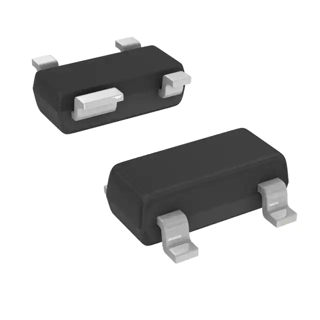
NPN EPITAXIAL SILICON TRANSISTOR
4-PIN MINI MOLD
PACKAGE DIMENSIONS (in mm)
• Ideal for medium-output applications
+0.2
100
mA
PT
200
mW
Junction Temperature
Tj
150
°C
Storage Temperature
Tstg
–65 to +150
°C
NT
Total Power Dissipation
SC
O
ELECTRICAL CHARACTERISTICS (TA = 25 °C)
PARAMETER
SYMBOL
TEST CONDITIONS
Collector Cut-off Current
ICBO
VCB = 5 V, IE = 0
Emitter Cut-off Current
IEBO
VEB = 1 V, IC = 0
DC Current Gain
Gain Bandwidth Product
Reverse Transfer Capacitance
Insertion Power Gain
Noise Figure
hFE
VCE = 3 V, IC = 30
fT
Cre
|S21e|
NF
mANote 1
+0.1
(1.9)
4
1
MIN.
TYP.
75
12.0
0.5
8.0
VCE = 3 V, IC = 7 mA, f = 2 GHz
MAX.
UNIT
0.1
µA
0.1
µA
150
MHzNote 2
VCE = 3 V, IC = 30 mA, f = 2 GHz
5°
PIN CONNECTIONS
1: Collector
2: Emitter
3: Base
4: Emitter
VCE = 3 V, IC = 30 mA, f = 2 GHz
VCB = 3 V, IE = 0, f = 1
2
5°
0.16
IC
0.4
V
VEBO
5°
+0.1
–0.06
2
Emitter to Base Voltage
+0.1
–0.05
V
VCEO
5°
0 to 0.1
6
Collector to Emitter Voltage
3
2
V
VCBO
+0.1
9
Collector to Base Voltage
0.6 –0.05
UNIT
+0.2
RATING
1.1–0.1
0.8
SYMBOL
IN
ABSOLUTE MAXIMUM RATINGS (TA = 25 °C)
PARAMETER
+0.2
1.5 –0.1
2.9 ± 0.2
(1.8)
0.85 0.95
• Can operate at low voltage
0.4 –0.05
+0.1
• Small reverse transfer capacitance
Collector Current
2.8 –0.3
0.4 –0.05
• High gain, low noise
GHz
0.7
10.0
1.5
pF
dB
2.5
dB
DI
Notes 1. Pulse measurement PW ≤ 350 µs, duty cycle ≤ 2 %
2. Collector to base capacitance measured by capacitance meter (automatic balance bridge method) when
emitter pin is connected to the guard pin.
Because this product uses high-frequency process, avoid excessive input of static electricity, etc.
The information in this document is subject to change without notice.
Document No. P13081EJ1V0DS00 (1st edition)
Date Published February 1998 N CP(K)
�NE67839 / 2SC5455
hFE CLASSIFICATION
100
180 μ A
160 μ A
140 μ A
120 μ A
100 μ A
15
80 μ A
60 μ A
40 μ A
IB = 20 μ A
10
5
1
2
3
4
5
6
DI
VCE - Collector to Emitter Voltage - V
2
25
0
200
200 μ A
0
50
0.5
VBE - DC Base Voltage - V
1.0
DC CURRENT GAIN vs. COLLECTOR CURRENT
SC
O
IC - Collector Current - mA
150
COLLECTOR CURRENT vs.
COLLECTOR TO EMITTER VOLTAGE
20
75 to 150
VCE = 3 V
NT
50
100
TA - Ambient Temperature - °C
25
hFE
IN
IC - Collector Current - mA
200
30
R55
UE
Free Air
35
Marking
COLLECTOR CURRENT vs. DC BASE VOLTAGE
60
7
DC Current Gain - hFE
PT - Total Power Dissipation - mW
TOTAL POWER DISSIPATION
vs. AMBIENT TEMPERATURE
40
FB
D
TYPICAL CHARACTERISTICS (TA = 25 °C)
0
RANK
VCE = 3 V
100
0
0.1 0.2
0.5
1
2
5
10 20
IC - Collector Current - mA
50 100
�NE67839 / 2SC5455
GAIN BANDWIDTH PRODUCT
vs. COLLECTOR CURRENT
10
8
6
4
2
2
5
10
20
50
IC - Collector Current - mA
VCE = 3 V
f = 2 GHz
14
12
10
Ga
8
6
4
NF
2
1
8
6
4
2
0
1
2
5
10
20
50
IC - Collector Current - mA
100
REVERSE TRANSFER CAPACITANCE
vs. COLLECTOR TO BASE VOLTAGE
IN
GAIN WITH MINIMUM NF/NOISE FIGURE
vs. COLLECTOR CURRENT
16
10
IC - Collector Current - mA
1
100
f = 1 MHZ
0.8
0.6
0.4
0.2
0
1
10
100
VCB - Collector to Base Voltage - V
DI
SC
O
0
100
10
Cre - Reverse Transfer Capacitance - pF
1
12
D
12
VCE = 3 V
f = 2 GHz
14
UE
|S21e| 2 - Insertion Power Gain - dB
14
0
Ga - Gain with Minimum NF - dB
NF - Noise Figure - dB
16
VCE = 3 V
f = 2 GHz
NT
fT - Gain Bandwidth Product - GHz
16
INSERTION POWER GAIN
vs. COLLECTOR CURRENT
3
�NE67839 / 2SC5455
24
VCE = 3 V
IC = 30 mA
20
20
|S21e|2
10
0
0.1
10
1
12
VCE = 3 V
IQ = 5 mA
f = 2 GHz
–4
–8
–20 –16
–10
–4
0
4
10
16
DI
SC
O
PIN - Input Power - dB
4
VCE = 3 V
IQ = 5 mA
f = 1 GHz
–8
–20
–16
–10
IN
16
0
0
NT
POUT - Output Power - dB
20
4
4
–4
0
4
PIN - Input Power - dB
OUTPUT POWER vs. INPUT POWER
8
8
–4
f - Frequency - GHz
24
12
UE
MAG
16
D
MSG
30
OUTPUT POWER vs. INPUT POWER
POUT - Output Power - dB
MAG - Maximum Available Gain - dB
MSG - Maximum Stable Gain - dB
|S21e|2 - Insertion Power Gain - dB
MAXIMUM AVAILABLE GAIN/
MAXIMUM STABLE GAIN/INSERTION
POWER GAIN vs. FREQUENCY
10
16
�NE67839 / 2SC5455
S PARAMETERS
VCE = 3.0 V, IC = 5.0 mA, Z0 = 50 Ω
MAG
–29.2
–55.4
–78.7
–97.0
–113.2
–127.0
–137.9
–147.8
–156.2
–163.6
–170.1
–176.2
178.4
173.4
168.7
164.5
160.5
156.8
153.0
149.9
146.4
143.5
140.5
137.6
135.1
132.4
130.3
127.7
125.7
123.3
14.200
12.643
11.179
9.470
8.319
7.339
6.450
5.764
5.176
4.717
4.318
3.974
3.673
3.429
3.202
2.984
2.831
2.669
2.523
2.396
2.268
2.162
2.044
1.952
1.870
1.773
1.712
1.632
1.561
1.494
S 21
ANG
MAG
159.5
142.7
128.9
118.4
107.7
100.0
93.3
87.3
82.2
77.3
72.9
68.7
64.7
60.7
57.1
53.5
49.9
46.5
42.7
39.6
36.1
32.9
29.9
26.7
24.4
21.2
18.2
15.9
12.6
10.7
0.026
0.046
0.060
0.069
0.074
0.078
0.080
0.082
0.083
0.084
0.085
0.086
0.086
0.087
0.089
0.090
0.091
0.093
0.095
0.097
0.099
0.102
0.104
0.108
0.111
0.115
0.120
0.124
0.129
0.133
ANG
MAG
153.2
132.8
118.6
108.8
99.9
93.3
87.8
82.9
78.4
74.3
70.6
66.9
63.6
59.9
56.9
53.5
50.3
47.4
44.0
41.1
38.1
35.1
32.4
29.6
27.4
24.8
21.8
19.7
16.9
15.0
0.023
0.039
0.048
0.053
0.057
0.060
0.063
0.066
0.069
0.072
0.075
0.079
0.082
0.085
0.089
0.092
0.096
0.100
0.103
0.107
0.111
0.115
0.118
0.122
0.126
0.131
0.136
0.140
0.146
0.149
S 12
ANG
MAG
74.3
60.0
49.1
41.5
36.6
32.3
30.4
28.7
26.9
26.3
25.4
25.9
26.2
26.3
26.8
27.3
28.1
29.2
29.7
30.6
31.2
31.6
32.7
33.4
34.1
34.6
35.2
34.7
34.5
34.3
0.948
0.849
0.742
0.644
0.569
0.511
0.462
0.427
0.395
0.374
0.358
0.343
0.334
0.326
0.322
0.321
0.316
0.319
0.319
0.323
0.328
0.333
0.341
0.346
0.357
0.369
0.384
0.393
0.412
0.418
ANG
MAG
69.0
55.1
46.1
41.7
39.5
38.6
38.2
38.1
38.4
38.8
38.8
39.4
39.9
40.0
39.9
39.9
40.1
40.1
39.8
40.0
39.6
39.1
39.0
38.7
38.7
38.1
37.6
36.8
35.8
35.3
0.898
0.737
0.597
0.496
0.423
0.375
0.332
0.307
0.285
0.269
0.257
0.249
0.244
0.241
0.240
0.243
0.244
0.248
0.251
0.255
0.266
0.268
0.281
0.283
0.299
0.306
0.326
0.332
0.350
0.356
S 22
ANG
–16.9
–32.0
–43.3
–52.7
–58.6
–64.0
–69.0
–73.1
–77.0
–80.9
–84.8
–88.1
–92.4
–96.2
–100.4
–103.9
–108.7
–111.9
–117.2
–119.9
–125.4
–127.0
–133.3
–133.8
–139.6
–140.4
–145.9
–148.1
–152.4
–155.2
D
0.849
0.792
0.732
0.688
0.640
0.613
0.594
0.581
0.574
0.570
0.569
0.570
0.574
0.577
0.583
0.589
0.596
0.603
0.610
0.617
0.624
0.632
0.637
0.645
0.646
0.654
0.660
0.666
0.673
0.676
ANG
UE
100.00
200.00
300.00
400.00
500.00
600.00
700.00
800.00
900.00
1000.00
1100.00
1200.00
1300.00
1400.00
1500.00
1600.00
1700.00
1800.00
1900.00
2000.00
2100.00
2200.00
2300.00
2400.00
2500.00
2600.00
2700.00
2800.00
2900.00
3000.00
S 11
IN
MAG
NT
FREQUENCY
MHz
VCE = 3.0 V, IC = 10.0 mA, Z0 = 50 Ω
MAG
100.00
200.00
300.00
400.00
500.00
600.00
700.00
800.00
900.00
1000.00
1100.00
1200.00
1300.00
1400.00
1500.00
1600.00
1700.00
1800.00
1900.00
2000.00
2100.00
2200.00
2300.00
2400.00
2500.00
2600.00
2700.00
2800.00
2900.00
3000.00
0.741
0.668
0.612
0.576
0.553
0.541
0.535
0.532
0.531
0.533
0.536
0.540
0.546
0.551
0.558
0.565
0.572
0.579
0.587
0.592
0.603
0.611
0.614
0.624
0.625
0.635
0.639
0.647
0.655
0.658
S 11
ANG
MAG
–41.6
–75.4
–101.6
–120.4
–135.2
–147.0
–156.6
–164.6
–171.5
–177.6
177.0
171.9
167.6
163.4
159.6
156.0
152.6
149.5
146.3
143.8
140.6
138.1
135.5
133.0
130.7
128.3
126.5
124.1
122.2
120.0
23.253
19.107
15.604
12.659
10.612
9.108
7.906
6.994
6.238
5.639
5.148
4.726
4.367
4.060
3.788
3.543
3.333
3.146
2.975
2.819
2.680
2.548
2.409
2.300
2.203
2.097
2.028
1.934
1.856
1.783
DI
SC
O
FREQUENCY
MHz
S 21
S 12
S 22
ANG
–25.2
–44.8
–58.1
–68.0
–74.5
–80.4
–86.3
–90.7
–95.6
–100.2
–105.1
–109.3
–114.2
–118.1
–123.1
–126.5
–131.6
–134.7
–140.5
–142.2
–148.0
–148.5
–154.5
–154.0
–159.2
–159.4
–164.0
–165.3
–168.9
–171.0
5
�NE67839 / 2SC5455
VCE = 3.0 V, IC = 20.0 mA, Z0 = 50 Ω
VCE = 3.0 V, IC = 30.0 mA, Z0 = 50 Ω
MAG
100.00
200.00
300.00
400.00
500.00
600.00
700.00
800.00
900.00
1000.00
1100.00
1200.00
1300.00
1400.00
1500.00
1600.00
1700.00
1800.00
1900.00
2000.00
2100.00
2200.00
2300.00
2400.00
2500.00
2600.00
2700.00
2800.00
2900.00
3000.00
0.540
0.512
0.500
0.503
0.500
0.502
0.508
0.511
0.516
0.521
0.526
0.533
0.539
0.545
0.553
0.559
0.567
0.572
0.582
0.587
0.594
0.603
0.607
0.618
0.617
0.628
0.633
0.641
0.648
0.652
–59.0
–99.3
–124.7
–142.0
–153.8
–163.0
–170.7
–177.0
177.7
172.7
168.4
164.1
160.4
156.8
153.4
150.3
147.4
144.6
141.8
139.6
136.7
134.6
132.0
129.8
127.7
125.5
123.9
121.5
119.9
117.7
33.348
24.680
18.769
14.726
12.083
10.226
8.816
7.760
6.889
6.214
5.654
5.188
4.795
4.447
4.162
3.883
3.660
3.453
3.253
3.086
2.917
2.784
2.638
2.509
2.409
2.287
2.216
2.119
2.033
1.959
ANG
MAG
–70.7
–112.4
–136.0
–150.9
–161.7
–169.8
–176.6
177.8
172.6
168.2
164.3
160.3
156.9
153.5
150.6
147.5
144.8
142.2
139.6
137.4
134.7
132.7
130.3
128.1
126.1
123.9
122.5
120.0
118.6
116.4
38.305
26.801
19.773
15.344
12.506
10.529
9.061
7.950
7.064
6.367
5.804
5.306
4.899
4.553
4.263
3.967
3.744
3.528
3.334
3.161
2.992
2.847
2.695
2.564
2.459
2.339
2.263
2.165
2.077
2.003
S 21
S 11
S 21
DI
SC
O
FREQUENCY
MHz
MAG
6
ANG
MAG
145.2
123.3
110.1
101.4
94.2
88.7
83.9
79.8
76.2
72.4
68.9
65.9
62.7
59.7
56.7
53.7
50.7
47.8
44.8
42.1
39.2
36.5
34.1
31.5
29.4
27.0
24.3
22.4
19.8
18.0
0.020
0.031
0.038
0.042
0.047
0.051
0.055
0.059
0.064
0.068
0.073
0.077
0.083
0.087
0.091
0.096
0.101
0.106
0.110
0.115
0.119
0.124
0.128
0.132
0.136
0.142
0.147
0.151
0.156
0.160
S 12
ANG
MAG
65.2
52.4
48.1
46.0
46.7
47.5
48.0
48.4
49.2
49.1
49.0
49.4
48.9
49.0
48.2
47.7
47.1
46.5
45.5
45.0
44.3
43.3
42.6
41.5
41.2
40.3
39.3
38.2
36.9
36.0
0.820
0.613
0.470
0.382
0.322
0.287
0.256
0.241
0.227
0.218
0.216
0.211
0.214
0.215
0.220
0.224
0.233
0.236
0.245
0.247
0.261
0.260
0.279
0.274
0.296
0.298
0.318
0.323
0.341
0.347
S 22
ANG
–35.6
–58.4
–73.0
–83.6
–91.6
–98.7
–105.3
–111.0
–116.8
–121.8
–127.6
–131.7
–136.8
–140.8
–146.1
–148.7
–153.2
–156.3
–161.2
–162.1
–166.9
–167.6
–172.6
–172.3
–175.9
–175.6
–179.5
179.6
177.1
175.1
D
0.608
0.556
0.527
0.505
0.510
0.508
0.509
0.512
0.516
0.521
0.525
0.531
0.538
0.544
0.551
0.557
0.566
0.571
0.580
0.586
0.594
0.602
0.607
0.617
0.617
0.628
0.633
0.641
0.647
0.651
ANG
UE
100.00
200.00
300.00
400.00
500.00
600.00
700.00
800.00
900.00
1000.00
1100.00
1200.00
1300.00
1400.00
1500.00
1600.00
1700.00
1800.00
1900.00
2000.00
2100.00
2200.00
2300.00
2400.00
2500.00
2600.00
2700.00
2800.00
2900.00
3000.00
S 11
IN
MAG
NT
FREQUENCY
MHz
ANG
MAG
140.7
118.8
106.5
98.5
91.8
86.8
82.3
78.4
74.9
71.5
68.3
65.2
62.2
59.2
56.4
53.5
50.4
47.8
44.8
42.3
39.4
36.8
34.4
31.8
29.9
27.6
24.8
23.1
20.5
18.9
0.019
0.028
0.033
0.037
0.043
0.048
0.053
0.057
0.062
0.068
0.073
0.078
0.083
0.088
0.093
0.098
0.104
0.108
0.113
0.118
0.123
0.128
0.132
0.136
0.140
0.146
0.150
0.155
0.160
0.164
S 12
ANG
MAG
63.3
51.9
49.4
51.0
51.3
52.1
52.6
52.8
53.0
53.6
53.1
53.2
52.2
51.8
51.2
50.8
49.5
48.2
47.4
46.6
45.5
44.4
43.5
42.9
42.0
40.9
40.0
38.9
37.4
36.1
0.773
0.547
0.415
0.337
0.285
0.256
0.234
0.222
0.213
0.208
0.207
0.207
0.211
0.213
0.221
0.226
0.233
0.241
0.251
0.251
0.268
0.265
0.285
0.280
0.302
0.302
0.326
0.328
0.346
0.352
S 22
ANG
–41.2
–65.8
–80.8
–92.0
–100.3
–107.8
–114.9
–120.7
–126.9
–132.0
–137.8
–142.0
–146.3
–150.9
–154.8
–157.3
–162.3
–164.1
–168.2
–169.9
–174.0
–175.0
–179.0
–178.5
177.6
177.7
174.6
173.7
171.5
169.7
�NE67839 / 2SC5455
VCE = 5.0 V, IC = 5.0 mA, Z0 = 50 Ω
MAG
–28.0
–53.2
–75.8
–93.6
–110.2
–123.8
–135.1
–145.2
–153.7
–161.3
–168.0
–174.2
–179.7
175.1
170.3
166.0
161.9
158.1
154.3
151.1
147.5
144.5
141.5
138.5
135.9
133.2
131.1
128.4
126.4
124.0
14.245
12.754
11.353
9.639
8.532
7.532
6.650
5.962
5.351
4.876
4.466
4.115
3.806
3.546
3.330
3.106
2.946
2.766
2.623
2.484
2.357
2.249
2.125
2.028
1.940
1.842
1.782
1.696
1.625
1.557
S 21
ANG
MAG
160.5
143.3
130.1
119.6
108.8
101.1
94.3
88.4
83.1
78.0
73.7
69.4
65.4
61.5
58.0
54.2
50.2
47.3
43.5
40.2
36.8
33.6
30.5
27.3
24.8
21.8
18.7
16.2
13.2
11.1
0.025
0.044
0.057
0.066
0.072
0.075
0.077
0.079
0.080
0.081
0.082
0.083
0.085
0.085
0.086
0.088
0.089
0.090
0.093
0.095
0.097
0.100
0.102
0.106
0.109
0.113
0.118
0.121
0.127
0.131
ANG
MAG
154.1
134.2
120.0
110.2
101.0
94.4
88.8
83.8
79.4
75.2
71.3
67.7
64.2
60.8
57.5
54.4
51.0
47.9
44.6
41.9
38.6
35.8
33.1
30.1
28.0
25.2
22.3
20.2
17.3
15.5
0.022
0.038
0.046
0.052
0.056
0.059
0.062
0.065
0.068
0.071
0.074
0.077
0.080
0.084
0.087
0.091
0.094
0.097
0.101
0.104
0.109
0.112
0.116
0.120
0.124
0.128
0.134
0.138
0.144
0.148
S 12
ANG
MAG
74.0
60.6
50.2
42.7
37.7
34.1
31.4
29.3
28.0
27.5
27.0
26.6
27.1
27.4
27.9
28.5
29.5
30.2
30.7
31.9
32.8
33.4
34.0
34.7
35.9
36.3
36.7
36.3
36.3
36.0
0.949
0.856
0.753
0.657
0.582
0.525
0.475
0.444
0.410
0.388
0.370
0.356
0.346
0.337
0.331
0.329
0.326
0.329
0.326
0.329
0.334
0.340
0.342
0.351
0.360
0.372
0.387
0.396
0.415
0.419
ANG
MAG
70.0
56.1
47.1
42.9
40.6
39.4
38.7
38.5
38.7
39.1
39.4
39.9
40.3
40.8
40.6
40.7
41.1
40.9
40.7
40.5
40.6
40.0
40.0
39.6
39.6
39.3
38.9
37.7
36.9
36.4
0.899
0.751
0.615
0.515
0.440
0.388
0.344
0.318
0.294
0.277
0.264
0.255
0.250
0.244
0.242
0.243
0.244
0.247
0.250
0.254
0.264
0.265
0.277
0.279
0.295
0.299
0.320
0.328
0.347
0.352
S 22
ANG
–16.1
–30.3
–41.4
–50.2
–56.0
–61.3
–66.2
–69.7
–73.9
–77.1
–81.0
–84.3
–88.2
–91.9
–96.0
–99.5
–104.1
–107.4
–112.9
–115.1
–121.1
–122.7
–128.6
–129.8
–135.2
–136.4
–142.2
–144.2
–148.4
–151.6
D
0.858
0.800
0.739
0.691
0.642
0.611
0.590
0.575
0.567
0.562
0.561
0.560
0.565
0.567
0.572
0.578
0.585
0.592
0.600
0.607
0.614
0.622
0.626
0.635
0.637
0.645
0.651
0.657
0.664
0.668
ANG
UE
100.00
200.00
300.00
400.00
500.00
600.00
700.00
800.00
900.00
1000.00
1100.00
1200.00
1300.00
1400.00
1500.00
1600.00
1700.00
1800.00
1900.00
2000.00
2100.00
2200.00
2300.00
2400.00
2500.00
2600.00
2700.00
2800.00
2900.00
3000.00
S 11
IN
MAG
NT
FREQUENCY
MHz
VCE = 5.0 V, IC = 10.0 mA, Z0 = 50 Ω
MAG
100.00
200.00
300.00
400.00
500.00
600.00
700.00
800.00
900.00
1000.00
1100.00
1200.00
1300.00
1400.00
1500.00
1600.00
1700.00
1800.00
1900.00
2000.00
2100.00
2200.00
2300.00
2400.00
2500.00
2600.00
2700.00
2800.00
2900.00
3000.00
0.756
0.680
0.616
0.578
0.548
0.532
0.532
0.520
0.518
0.520
0.522
0.525
0.531
0.536
0.543
0.550
0.558
0.564
0.573
0.578
0.587
0.596
0.601
0.611
0.612
0.622
0.627
0.635
0.642
0.647
S 11
ANG
MAG
–39.2
–71.6
–97.0
–116.3
–131.4
–143.4
–153.4
–161.6
–168.8
–175.2
179.2
174.0
169.5
165.1
161.2
157.5
154.1
150.9
147.7
145.0
141.8
139.4
136.6
134.0
131.7
129.2
127.5
125.0
123.1
120.9
23.248
19.314
15.939
12.974
10.940
9.424
8.187
7.256
6.480
5.861
5.342
4.906
4.535
4.213
3.949
3.685
3.483
3.289
3.098
2.942
2.791
2.646
2.515
2.396
2.302
2.189
2.116
2.020
1.936
1.861
DI
SC
O
FREQUENCY
MHz
S 21
S 12
S 22
ANG
–23.7
–42.3
–55.1
–64.5
–70.8
–76.2
–81.1
–85.8
–90.3
–94.3
–98.9
–102.7
–107.3
–111.7
–116.3
–120.2
–125.0
–128.5
–134.3
–136.1
–141.7
–142.7
–149.1
–148.5
–153.8
–154.0
–159.2
–160.8
–164.3
–166.7
7
�NE67839 / 2SC5455
VCE = 5.0 V, IC = 20.0 mA, Z0 = 50 Ω
VCE = 5.0 V, IC = 30.0 mA, Z0 = 50 Ω
MAG
100.00
200.00
300.00
400.00
500.00
600.00
700.00
800.00
900.00
1000.00
1100.00
1200.00
1300.00
1400.00
1500.00
1600.00
1700.00
1800.00
1900.00
2000.00
2100.00
2200.00
2300.00
2400.00
2500.00
2600.00
2700.00
2800.00
2900.00
3000.00
0.572
0.521
0.496
0.487
0.485
0.484
0.486
0.489
0.493
0.499
0.504
0.510
0.516
0.522
0.529
0.536
0.544
0.551
0.560
0.565
0.574
0.583
0.586
0.599
0.599
0.611
0.614
0.623
0.631
0.635
–54.4
–93.3
–118.9
–136.8
–149.4
–159.3
–167.5
–174.2
179.8
174.5
170.0
165.6
161.8
158.1
154.7
151.5
148.7
145.9
143.0
140.7
137.8
135.7
133.1
130.8
128.7
126.5
124.9
122.4
120.9
118.6
33.512
25.234
19.353
15.238
12.561
10.646
9.192
8.090
7.203
6.487
5.907
5.426
5.010
4.651
4.343
4.071
3.819
3.607
3.402
3.235
3.060
2.916
2.763
2.631
2.524
2.407
2.325
2.226
2.135
2.057
ANG
MAG
–64.3
–105.1
–129.7
–146.1
–157.1
–166.1
–173.3
–179.3
175.2
170.5
166.5
162.3
158.9
155.3
152.2
149.2
146.4
143.8
141.0
138.9
136.0
134.3
131.6
129.5
127.4
125.2
123.7
121.3
119.8
117.6
38.635
27.544
20.521
15.977
13.055
11.019
9.493
8.343
7.411
6.670
6.077
5.575
5.148
4.785
4.465
4.169
3.928
3.715
3.496
3.326
3.136
2.992
2.835
2.700
2.599
2.462
2.382
2.285
2.188
2.115
S 21
S 11
S 21
DI
SC
O
FREQUENCY
MHz
MAG
8
ANG
MAG
146.5
124.9
111.5
102.7
95.2
89.6
84.9
80.6
76.9
73.1
69.8
66.6
63.5
60.3
57.4
54.4
51.4
48.5
45.5
42.9
40.1
37.2
34.7
32.0
30.0
27.7
24.8
22.9
20.2
18.5
0.020
0.031
0.037
0.042
0.046
0.050
0.054
0.058
0.062
0.068
0.072
0.076
0.081
0.086
0.090
0.095
0.099
0.103
0.108
0.112
0.117
0.121
0.126
0.130
0.134
0.139
0.144
0.149
0.154
0.158
S 12
ANG
MAG
66.2
53.6
48.0
47.5
47.1
47.4
48.0
48.6
49.0
49.6
49.5
49.2
48.9
49.0
48.4
48.0
47.6
46.7
46.2
45.3
44.8
43.7
43.2
42.4
41.7
41.1
40.3
39.0
37.8
36.8
0.830
0.630
0.485
0.395
0.332
0.294
0.263
0.243
0.229
0.219
0.213
0.208
0.209
0.208
0.211
0.216
0.221
0.224
0.234
0.236
0.249
0.250
0.266
0.264
0.284
0.285
0.308
0.314
0.331
0.337
S 22
ANG
–33.2
–55.1
–69.0
–79.0
–86.2
–92.5
–98.6
–103.6
–109.7
–114.4
–119.6
–124.6
–129.5
–133.9
–138.7
–141.7
–146.9
–149.5
–154.6
–156.4
–161.6
–162.2
–167.5
–166.9
–171.1
–170.9
–175.1
–175.8
–178.6
179.3
D
0.635
0.566
0.526
0.505
0.498
0.493
0.492
0.494
0.497
0.501
0.505
0.511
0.518
0.524
0.531
0.537
0.546
0.552
0.561
0.567
0.576
0.585
0.589
0.600
0.601
0.611
0.616
0.625
0.632
0.636
ANG
UE
100.00
200.00
300.00
400.00
500.00
600.00
700.00
800.00
900.00
1000.00
1100.00
1200.00
1300.00
1400.00
1500.00
1600.00
1700.00
1800.00
1900.00
2000.00
2100.00
2200.00
2300.00
2400.00
2500.00
2600.00
2700.00
2800.00
2900.00
3000.00
S 11
IN
MAG
NT
FREQUENCY
MHz
ANG
MAG
142.3
120.4
107.8
99.8
92.9
87.8
83.2
79.4
75.8
72.2
69.0
66.0
63.1
60.0
57.2
54.4
51.4
48.6
45.7
43.0
40.2
37.7
35.1
32.5
30.7
28.1
25.6
23.9
21.2
19.5
0.018
0.028
0.033
0.038
0.043
0.047
0.052
0.057
0.062
0.067
0.072
0.077
0.082
0.086
0.092
0.097
0.101
0.106
0.111
0.115
0.120
0.125
0.129
0.134
0.138
0.143
0.148
0.153
0.158
0.162
S 12
ANG
MAG
64.8
53.5
50.0
50.1
50.5
51.4
52.7
52.8
53.3
53.1
53.2
52.6
52.7
51.9
51.1
50.6
49.8
48.9
47.9
47.1
46.4
45.1
44.4
43.3
42.7
41.7
40.7
39.4
38.1
37.0
0.780
0.567
0.427
0.346
0.291
0.260
0.235
0.219
0.210
0.205
0.200
0.199
0.203
0.204
0.209
0.213
0.221
0.224
0.235
0.239
0.253
0.251
0.268
0.265
0.288
0.288
0.310
0.316
0.331
0.338
S 22
ANG
–38.5
–61.5
–75.6
–86.2
–94.3
–100.7
–107.4
–113.0
–119.7
–124.6
–130.2
–135.0
–139.3
–143.3
–147.8
–151.5
–155.4
–158.4
–163.5
–164.2
–168.8
–169.9
–174.6
–173.3
–177.8
–177.6
178.8
178.0
175.3
173.9
�NOTICE
Descriptions of circuits, software and other related information in this document are provided only to illustrate the operation of semiconductor products and
application examples. You are fully responsible for the incorporation of these circuits, software, and information in the design of your equipment. California
Eastern Laboratories and Renesas Electronics assumes no responsibility for any losses incurred by you or third parties arising from the use of these circuits,
software, or information.
2.
California Eastern Laboratories has used reasonable care in preparing the information included in this document, but California Eastern Laboratories does
not warrant that such information is error free. California Eastern Laboratories and Renesas Electronics assumes no liability whatsoever for any damages
incurred by you resulting from errors in or omissions from the information included herein.
3.
California Eastern Laboratories and Renesas Electronics do not assume any liability for infringement of patents, copyrights, or other intellectual property
rights of third parties by or arising from the use of Renesas Electronics products or technical information described in this document. No license, express,
implied or otherwise, is granted hereby under any patents, copyrights or other intellectual property rights of California Eastern Laboratories or Renesas
Electronics or others.
4.
You should not alter, modify, copy, or otherwise misappropriate any Renesas Electronics product, whether in whole or in part. California Eastern
Laboratories and Renesas Electronics assume no responsibility for any losses incurred by you or third parties arising from such alteration, modification, copy
or otherwise misappropriation of Renesas Electronics product.
5.
Renesas Electronics products are classified according to the following two quality grades: “Standard” and “High Quality”. The recommended applications
for each Renesas Electronics product depends on the product’s quality grade, as indicated below. “Standard”: Computers; office equipment; communications
equipment; test and measurement equipment; audio and visual equipment; home electronic appliances; machine tools; personal electronic equipment; and
industrial robots etc. “High Quality”: Transportation equipment (automobiles, trains, ships, etc.); traffic control systems; anti-disaster systems; anti-crime
systems; and safety equipment etc. Renesas Electronics products are neither intended nor authorized for use in products or systems that may pose a direct
threat to human life or bodily injury (artificial life support devices or systems, surgical implantations etc.), or may cause serious property damages (nuclear
reactor control systems, military equipment etc.). You must check the quality grade of each Renesas Electronics product before using it in a particular
application. You may not use any Renesas Electronics product for any application for which it is not intended. California Eastern Laboratories and Renesas
Electronics shall not be in any way liable for any damages or losses incurred by you or third parties arising from the use of any Renesas Electronics product
for which the product is not intended by California Eastern Laboratories or Renesas Electronics.
6.
You should use the Renesas Electronics products described in this document within the range specified by California Eastern Laboratories, especially with
respect to the maximum rating, operating supply voltage range, movement power voltage range, heat radiation characteristics, installation and other product
characteristics. California Eastern Laboratories shall have no liability for malfunctions or damages arising out of the use of Renesas Electronics products
beyond such specified ranges.
7.
Although Renesas Electronics endeavors to improve the quality and reliability of its products, semiconductor products have specific characteristics such as
the occurrence of failure at a certain rate and malfunctions under certain use conditions. Further, Renesas Electronics products are not subject to radiation
resistance design. Please be sure to implement safety measures to guard them against the possibility of physical injury, and injury or damage caused by
fire in the event of the failure of a Renesas Electronics product, such as safety design for hardware and software including but not limited to redundancy,
fire control and malfunction prevention, appropriate treatment for aging degradation or any other appropriate measures. Because the evaluation of
microcomputer software alone is very difficult, please evaluate the safety of the final products or systems manufactured by you.
8.
Please contact a California Eastern Laboratories sales office for details as to environmental matters such as the environmental compatibility of each Renesas
Electronics product. Please use Renesas Electronics products in compliance with all applicable laws and regulations that regulate the inclusion or use of
controlled substances, including without limitation, the EU RoHS Directive. California Eastern Laboratories and Renesas Electronics assume no liability for
damages or losses occurring as a result of your noncompliance with applicable laws and regulations.
9.
Renesas Electronics products and technology may not be used for or incorporated into any products or systems whose manufacture, use, or sale is prohibited
under any applicable domestic or foreign laws or regulations. You should not use Renesas Electronics products or technology described in this document
for any purpose relating to military applications or use by the military, including but not limited to the development of weapons of mass destruction. When
exporting the Renesas Electronics products or technology described in this document, you should comply with the applicable export control laws and
regulations and follow the procedures required by such laws and regulations.
10. It is the responsibility of the buyer or distributor of California Eastern Laboratories, who distributes, disposes of, or otherwise places the Renesas Electronics
product with a third party, to notify such third party in advance of the contents and conditions set forth in this document, California Eastern Laboratories and
Renesas Electronics assume no responsibility for any losses incurred by you or third parties as a result of unauthorized use of Renesas Electronics products.
11. This document may not be reproduced or duplicated in any form, in whole or in part, without prior written consent of California Eastern Laboratories.
12. Please contact a California Eastern Laboratories sales office if you have any questions regarding the information contained in this document or Renesas
Electronics products, or if you have any other inquiries.
SC
O
NT
IN
UE
D
1.
NOTE 1: “Renesas Electronics” as used in this document means Renesas Electronics Corporation and also includes its majority-owned subsidiaries.
NOTE 2: “Renesas Electronics product(s)” means any product developed or manufactured by or for Renesas Electronics.
NOTE 3: Products and product information are subject to change without notice.
DI
CEL Headquarters • 4590 Patrick Henry Drive, Santa Clara, CA 95054 • Phone (408) 919-2500 • www.cel.com
For a complete list of sales offices, representatives and distributors,
Please visit our website: www.cel.com/contactus
�