NEC's MEDIUM POWER NPN
NE678M04
SILICON HIGH FREQUENCY TRANSISTOR
FEATURES
•
NEW LOW PROFILE M04 PACKAGE:
SOT-343 footprint, with a height of only 0.59 mm
Flat lead style for better RF performance
+0.40-0.05
2
1.25
0.650.65
2.0±0.1
R55
1
NEC's NE678M04 is fabricated using NEC's HFT3 wafer
process. With a transition frequency of 12 GHz, the NE678M04
is usable in applications from 100 MHz to 3 GHz. The NE678M04
provides P1dB of 18 dBm, even with low voltage and low
current, making this device an excellent choice for the driver
stage for mobile or fixed wireless applications.
+0.01
0.59±0.05
+0.30-0.05 (leads 1, 3 and ,4)
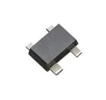
The NE678M04 is housed in NEC's new low profile/flat lead
style "M04" package
ELECTRICAL CHARACTERISTICS (TA = 25°C)
+0.1
DESCRIPTION
2.05±0.1
1.25±0.1
PIN CONNECTIONS
1. Emitter
2. Collector
3. Emitter
4. Base
PART NUMBER
PACKAGE OUTLINE
EIAJ3 REGISTRATION NUMBER
DC
SYMBOLS
PARAMETERS AND CONDITIONS
UNITS
Collector Cutoff Current at VCB = 5V, IE = 0
nA
IEBO
Emitter Cutoff Current at VEB = 1 V, IC = 0
nA
hFE
DC Current1 Gain at VCE = 3 V, IC = 30 mA
P1dB
Output Power at 1 dB compression point at VCE = 2.8 V, ICQ = 10 mA,
f = 1.8 GHz, Pin = 7 dBm
GL
RF
NE678M04
M04
2SC5753
ICBO
Linear Gain at VCE = 2.8 V, IC = 10 mA, f = 1.8 GHz, Pin = -5 dBm
Maximum Available Gain4 at VCE = 3 V, IC = 30 mA, f = 2 GHz
MAG
|S21E|2
ηc
Noise Figure at VCE = 3 V, IC = 7 mA, f = 2 GHz, ZS = Zopt
Reverse Transfer Capacitance2 at VCB = 3 V, IC = 0, f = 1 MHz
Cre
100
120
dB
13.0
dBm
13.5
%
MAX
100
18.0
dB
Gain Bandwidth at VCE = 3 V, IC = 30 mA, f = 2 GHz
TYP
dBm
Collector Efficiency at VCE = 2.8 V, ICQ = 10 mA, f = 1.8 GHz,
Pin = 7 dBm
fT
MIN
75
Insertion Power Gain at VCE = 3 V, IC = 30 mA, f = 2 GHz
NF
1.30
HIGH LINEAR GAIN:
GL = 13 dB at 1.8 GHz
+0.11-0.05
•
3
HIGH OUTPUT POWER:
P-1dB = 18 dBm at 1.8 GHz
0.650.65
•
4
HIGH GAIN BANDWIDTH:
fT = 12 GHz
+0.30
•
8.0
150
10.5
55
dB
1.7
GHz
12.0
pF
0.42
2.5
0.7
Notes:
1. Pulsed measurement, pulse width ≤ 350 µs, duty cycle ≤ 2 %.
2. Collector to Base capacitance measured by capacitance meter(automatic balance bridge method) when emitter pin is connected to the
guard pin of capacitance meter.
3. Electronic Industrail Association of Japan.
4. MAG = |S21|
|S12|
(K ±
K 2- 1
).
California Eastern Laboratories
�NE678M04
ABSOLUTE MAXIMUM RATINGS1 (TA = 25°C)
ORDERING INFORMATION
SYMBOLS
PARAMETERS
UNITS
RATINGS
PART NUMBER
QUANTITY
VCBO
Collector to Base Voltage
V
9.0
NE678M04-T2-A
3k pcs./reel
VCEO
Collector to Emitter Voltage
V
6.0
VEBO
Emitter to Base Voltage
V
2.0
IC
Collector Current
mA
100
PT
Total Power Dissipation2
mW
205
TJ
Junction Temperature
°C
150
TSTG
Storage Temperature
°C
-65 to +150
Note:
1. Operation in excess of any one of these parameters may result
in permanent damage.
2. Mounted on a 1.08cm2 x 1.0 mm thick glass epoxy PCB.
THERMAL RESISTANCE
SYMBOLS
PARAMETERS
UNITS
RATINGS
Rth j-a
Thermal Resistance from
Junction to Ambient
°C/W
600
Note:
1. Mounted on a 1.08cm2 x 1.0 mm thick glass epoxy PCB.
TYPICAL PERFORMANCE CURVES (TA = 25 °C)
TOTAL POWER DISSIPATION
vs. AMBIENT TEMPERATURE
REVERSE TRANSFER CAPACITANCE
vs. COLLECTOR TO BASE VOLTAGE
Reverse Transfer Capacitance Cre (pF)
Total Power Dissipation Pout (mW)
300
Mounted on Glass Epoxy PCB
2
(1.08 cm x 1.0 mm (t) )
250
205
200
150
100
50
0
25
50
75
100
125
150
f= 1 MHz
0.9
0.8
0.7
0.6
0.5
0.4
0.3
0.2
0.1
0
1
2
3
4
6
5
Ambient Temperature TA (ºC)
Collector to Base Voltage VCB (V)
COLLECTOR CURRENT
vs. COLLECTOR TO EMITTER VOLTAGE
DC CURRENT GAIN
vs. COLLECTOR CURRENT
1000
100
VCE = 3 V
90
700 µA
80
600 µA
70
DC Current Gain (hFE)
Collector Current IC (mA)
1.0
500 µA
60
400 µA
50
300 µA
40
200 µA
30
100
20
10
0
IB =100 µA
2
4
6
Collector to Emitter Voltage VCE (V)
8
10
0.1
1
10
Collector Current IC (mA)
100
�NE678M04
TYPICAL PERFORMANCE CURVES (TA = 25 °C)
GAIN BANDWIDTH PRODUCT
vs. COLLECTOR CURRENT
10
5
Insertion Power Gain |S21e|2, (dB)
Maximum Available Power Gain MAG (dB)
10
100
VCE = 3 V
IC = 30 mA
30
MSG
MAG
25
20
15
10
|S21e|2
5
0
0.1
1
10
Collector Current IC (mA)
Frequency f (mA)
INSERTION POWER GAIN,
MAG, MSG vs. COLLECTOR CURRENT
INSERTION POWER GAIN,
MAG, MSG vs. COLLECTOR CURRENT
25
VCE = 3 V
f = 1 GHz
MSG
MAG
20
15
|S21e|2
10
5
0
1
10
100
Insertion Power Gain |S21e|2, (dB)
Maximum Available Power Gain MAG (dB)
Maximum Stable Power Gain MSG (dB)
Insertion Power Gain |S21e|2, (dB)
Maximum Available Power Gain MAG (dB)
Maximum Stable Power Gain MSG (dB)
0
1
35
25
VCE = 3 V
f = 2 GHz
20
MAG
10
|S21e|2
5
0
1
10
100
Collector Current IC (mA)
Collector Current IC (mA)
INSERTION POWER GAIN,
MAG vs. COLLECTOR CURRENT
NOISE FIGURE, ASSOCIATED GAIN
vs. COLLECTOR CURRENT
8
25
VCE = 3 V
f = 2.5 GHz
16
VCE = 3 V
f = 2 GHz
Ga
20
15
MAG
10
|S21e|2
5
0
MSG
15
6
12
4
8
4
2
NF
1
10
Collector Current IC (mA)
100
0
1
10
Collector Current IC (mA)
0
100
Associated Gain Ga (dB)
VCE = 3 V
f = 2 GHz
Noise Figure NF (dB)
Gain Bandwidth Product fT (GHz)
15
Insertion Power Gain |S21e|2, (dB)
Maximum Available Power Gain MAG (dB)
Maximum Stable Power Gain MSG (dB)
INSERTION POWER GAIN,
MAG, MSG vs. FREQUENCY
�NE678M04
TYPICAL PERFORMANCE CURVES (TA = 25 °C)
OUTPUT POWER, POWER GAIN,
COLLECTOR CURRENT, COLLECTOR
EFFICIENCY vs. INPUT POWER
25 VCE = 3.2 V
250
Output Power Pout (dbm)
Power Gain Gp (dB)
200
20
GP
15
10
150
100
IC
5
50
ηC
0
-10
-5
0
5
10
Collector Current IC (mA),
Collector Efficiency ηc (%)
Pout
f = 0.9 GHz
Icq = 10 mA (RF OFF)
0
15
Input Power Pin (dBm)
OUTPUT POWER, POWER GAIN,
COLLECTOR CURRENT, COLLECTOR
EFFICIENCY vs. INPUT POWER
20
250
Pout
200
15
150
GP
10
100
ηC
5
50
25
Output Power Pout (dbm)
Power Gain Gp (dB)
VCE = 2.8 V
f = 1.8 GHz
Icq = 10 mA (RF OFF)
Collector Current IC (mA),
Collector Efficiency ηc (%)
Output Power Pout (dbm)
Power Gain Gp (dB)
25
20
250
VCE = 3.2 V
f = 1.8 GHz
Icq = 10 mA (RF OFF)
-5
0
150
GP
10
100
ηC
5
50
IC
5
10
0
15
0
-10
OUTPUT POWER, POWER GAIN,
COLLECTOR CURRENT, COLLECTOR
EFFICIENCY vs. INPUT POWER
20
250
Pout
200
15
150
GP
10
100
ηC
5
50
IC
0
-10
-5
0
5
10
Input Power Pin (dBm)
0
15
Collector Current IC (mA),
Collector Efficiency ηc (%)
Output Power Pout (dbm)
Power Gain Gp (dB)
25
-5
0
5
10
Input Power Pin (dBm)
Input Power Pin (dBm)
VCE = 3.2 V
f = 2.4 GHz
Icq = 10 mA (RF OFF)
200
15
IC
0
-10
Pout
0
15
Collector Current IC (mA),
Collector Efficiency ηc (%)
OUTPUT POWER, POWER GAIN,
COLLECTOR CURRENT, COLLECTOR
EFFICIENCY vs. INPUT POWER
�NE678M04
TYPICAL SCATTERING PARAMETERS (TA = 25°C)
+90º
j50
j100
j25
j10
0
+45º
+135º
S22
25
10
5 10 15 20
50 100
+0º
+180º
S11
-j10
-45º
-135º
-j100
-j25
-90º
-j50
NE678M04
VC = 2 V, IC = 10 mA
FREQUENCY
S11
GHz
MAG
0.100
0.200
0.300
0.400
0.500
0.600
0.700
0.800
0.900
1.000
1.500
1.800
1.900
2.000
2.500
3.000
3.500
4.000
4.500
5.000
5.500
6.000
0.72
0.68
0.65
0.63
0.62
0.60
0.60
0.60
0.60
0.60
0.59
0.59
0.59
0.59
0.59
0.60
0.61
0.63
0.65
0.67
0.69
0.71
S21
ANG
-45.97
-81.43
-106.66
-124.06
-136.69
-148.20
-155.78
-161.77
-167.38
-171.69
170.30
161.69
158.90
156.19
142.62
128.82
114.69
101.16
89.04
78.45
68.99
59.90
MAG
23.42
19.17
15.41
12.56
10.53
8.85
7.72
6.86
6.15
5.59
3.81
3.21
3.05
2.90
2.35
1.97
1.69
1.47
1.29
1.15
1.02
0.92
S12
ANG
152.40
132.28
118.19
108.21
100.63
94.98
89.80
85.45
81.38
77.66
61.44
52.84
50.05
47.32
33.99
21.32
9.12
-2.44
-13.44
-23.86
-33.79
-43.00
MAG
0.02
0.04
0.05
0.05
0.06
0.06
0.06
0.06
0.07
0.07
0.08
0.09
0.09
0.09
0.11
0.13
0.14
0.16
0.18
0.19
0.21
0.23
S22
ANG
MAG
65.62
52.02
42.17
37.11
33.66
32.53
31.81
31.70
31.29
31.31
33.17
33.52
33.69
33.45
32.55
29.86
26.40
21.89
16.66
10.92
4.77
-1.43
0.90
0.74
0.61
0.52
0.46
0.38
0.36
0.34
0.33
0.32
0.31
0.32
0.32
0.33
0.36
0.39
0.43
0.47
0.50
0.53
0.57
0.60
K
ANG
-29.51
-51.31
-66.86
-77.84
-86.27
-92.24
-98.70
-102.52
-106.64
-110.16
-123.84
-130.08
-131.91
-133.96
-142.01
-149.47
-156.17
-163.41
-171.39
179.62
170.14
160.66
MAG1
(dB)
0.10
0.18
0.26
0.34
0.42
0.56
0.62
0.68
0.74
0.79
1.00
1.07
1.10
1.11
1.14
1.15
1.12
1.07
1.03
0.98
0.94
0.92
29.97
26.71
24.93
23.61
22.62
21.75
21.00
20.32
19.72
19.17
16.81
13.98
13.41
12.93
11.02
9.63
8.62
7.95
7.59
7.69
6.86
6.09
Note:
1. Gain Calculations:
MAG =
|S21|
|S12|
(K –
K 2- 1
). When K ≥ 1, MAG is undefined and MSG values are used. MSG =
MAG = Maximum Available Gain
MSG = Maximum Stable Gain
2
2
2
|S21|
, K = 1 + | ∆ | - |S11| - |S22| , ∆ = S11 S22 - S21 S12
|S12|
2 |S12 S21|
�NE678M04
TYPICAL SCATTERING PARAMETERS (TA = 25°C)
j50
+90º
j100
j25
j10
0
+45º
+135º
S11
25
10
10 20 30
50 100
S22
+0º
+180º
-j10
-45º
-135º
-j100
-j25
-90º
-j50
NE678M04
VC = 3 V, IC = 30 mA
FREQUENCY
S11
GHz
MAG
0.100
0.200
0.300
0.400
0.500
0.600
0.700
0.800
0.900
1.000
1.500
1.800
1.900
2.000
2.500
3.000
3.500
4.000
4.500
5.000
5.500
6.000
0.52
0.55
0.56
0.56
0.56
0.56
0.57
0.57
0.57
0.57
0.57
0.57
0.57
0.57
0.57
0.57
0.58
0.60
0.62
0.64
0.65
0.67
S21
ANG
-74.30
-114.70
-136.33
-149.34
-158.35
-167.02
-172.39
-176.68
179.14
176.07
161.30
153.82
151.23
148.83
136.19
123.25
109.78
96.93
85.43
75.45
66.54
57.90
MAG
39.85
28.29
20.98
16.42
13.45
11.22
9.70
8.57
7.66
6.93
4.70
3.96
3.76
3.58
2.90
2.44
2.10
1.84
1.63
1.46
1.32
1.19
S12
ANG
141.89
120.64
108.33
100.26
94.25
90.08
85.86
82.27
78.87
75.71
61.65
53.96
51.43
48.96
36.74
24.91
13.41
2.30
-8.43
-18.79
-28.80
-38.45
MAG
0.02
0.03
0.03
0.03
0.04
0.04
0.04
0.05
0.05
0.06
0.08
0.09
0.09
0.10
0.12
0.14
0.16
0.18
0.19
0.21
0.22
0.24
S22
ANG
MAG
63.14
50.10
45.90
45.26
45.86
47.13
48.18
49.01
49.82
50.22
49.69
48.26
47.59
46.86
42.26
36.84
30.78
24.27
17.67
11.05
4.47
-2.21
0.79
0.58
0.46
0.40
0.36
0.30
0.28
0.27
0.27
0.26
0.27
0.27
0.28
0.28
0.31
0.34
0.37
0.40
0.43
0.47
0.50
0.53
K
ANG
-43.24
-69.59
-86.51
-97.94
-106.44
-115.48
-121.83
-125.22
-128.89
-131.89
-142.80
-147.21
-148.33
-149.67
-154.80
-159.87
-164.45
-170.06
-176.72
175.39
166.91
158.44
MAG1
(dB)
0.22
0.37
0.49
0.61
0.69
0.83
0.88
0.92
0.96
0.98
1.07
1.09
1.09
1.09
1.09
1.08
1.06
1.04
1.01
0.98
0.95
0.93
33.48
30.30
28.27
26.78
25.46
24.40
23.43
22.51
21.72
20.95
16.35
14.70
14.25
13.81
12.03
10.71
9.71
9.03
8.78
8.46
7.72
7.05
Note:
1. Gain Calculations:
MAG =
|S21|
|S12|
(K –
K 2- 1
). When K ≥ 1, MAG is undefined and MSG values are used. MSG =
MAG = Maximum Available Gain
MSG = Maximum Stable Gain
2
2
2
|S21|
, K = 1 + | ∆ | - |S11| - |S22| , ∆ = S11 S22 - S21 S12
|S12|
2 |S12 S21|
�NE678M04
TYPICAL SCATTERING PARAMETERS (TA = 25°C)
+90º
j50
j100
j25
j10
0
+45º
+135º
S11
10 20 30 40
25 50 100
10
+0º
+180º
S22
-j10
-45º
-135º
-j100
-j25
-j50
-90º
NE678M04
VC = 5 V, IC = 70 mA
FREQUENCY
S11
GHz
MAG
0.100
0.200
0.300
0.400
0.500
0.600
0.700
0.800
0.900
1.000
1.500
1.800
1.900
2.000
2.500
3.000
3.500
4.000
4.500
5.000
5.500
6.000
0.46
0.51
0.53
0.54
0.55
0.55
0.56
0.56
0.56
0.56
0.56
0.55
0.55
0.55
0.55
0.56
0.57
0.58
0.60
0.62
0.64
0.65
S21
ANG
-92.27
-129.65
-147.72
-158.40
-165.77
-173.25
-177.75
178.53
174.86
172.16
158.57
151.40
148.96
146.64
134.28
121.53
108.26
95.62
84.34
74.53
65.76
57.22
MAG
47.62
31.64
22.84
17.67
14.38
11.98
10.33
9.12
8.14
7.36
4.98
4.19
3.98
3.79
3.07
2.58
2.22
1.95
1.73
1.55
1.40
1.27
S12
ANG
136.35
115.69
104.50
97.25
91.83
88.17
84.28
80.93
77.76
74.77
61.30
53.86
51.41
49.00
37.07
25.46
14.13
3.18
-7.49
-17.79
-27.80
-37.47
MAG
0.01
0.02
0.03
0.03
0.03
0.04
0.04
0.04
0.05
0.05
0.08
0.09
0.09
0.10
0.12
0.14
0.16
0.18
0.20
0.21
0.22
0.24
S22
ANG
MAG
61.08
51.85
50.27
51.38
53.36
54.92
55.88
56.52
56.38
57.10
55.00
52.53
51.60
50.56
44.90
38.56
32.10
25.40
18.42
11.57
4.84
-1.99
0.69
0.49
0.39
0.34
0.31
0.26
0.25
0.25
0.24
0.24
0.25
0.26
0.26
0.27
0.29
0.32
0.36
0.39
0.42
0.45
0.48
0.51
K
ANG
-50.06
-77.41
-94.24
-105.50
-113.55
-123.64
-129.49
-132.28
-135.41
-138.20
-147.24
-150.84
-151.75
-152.82
-157.03
-161.31
-165.52
-170.85
-177.21
175.01
166.70
158.43
MAG1
(dB)
0.35
0.51
0.65
0.76
0.84
0.94
0.98
1.00
1.02
1.04
1.08
1.09
1.09
1.09
1.09
1.07
1.06
1.03
1.01
0.98
0.96
0.94
35.14
31.73
29.60
27.89
26.43
25.20
24.08
22.69
21.26
20.18
16.43
14.89
14.44
14.02
12.29
10.96
9.97
9.29
9.02
8.67
7.95
7.29
Note:
1. Gain Calculations:
MAG =
|S21|
|S12|
(K –
K 2- 1
). When K ≥ 1, MAG is undefined and MSG values are used. MSG =
2
2
2
|S21|
, K = 1 + | ∆ | - |S11| - |S22| , ∆ = S11 S22 - S21 S12
|S12|
2 |S12 S21|
MAG = Maximum Available Gain
MSG = Maximum Stable Gain
Life Support Applications
These NEC products are not intended for use in life support devices, appliances, or systems where the malfunction of these products can reasonably
be expected to result in personal injury. The customers of CEL using or selling these products for use in such applications do so at their own risk and
agree to fully indemnify CEL for all damages resulting from such improper use or sale.
EXCLUSIVE NORTH AMERICAN AGENT FOR NEC RF, MICROWAVE & OPTOELECTRONIC SEMICONDUCTORS
CALIFORNIA EASTERN LABORATORIES • Headquarters • 4590 Patrick Henry Drive • Santa Clara, CA 95054-1817 • (408) 988-3500 • Telex 34-6393 • FAX (408) 988-0279
DATA SUBJECT TO CHANGE WITHOUT NOTICE
Internet: http://WWW.CEL.COM
02/07/2002
�4590 Patrick Henry Drive
Santa Clara, CA 95054-1817
Telephone: (408) 919-2500
Facsimile: (408) 988-0279
Subject: Compliance with EU Directives
CEL certifies, to its knowledge, that semiconductor and laser products detailed below are compliant
with the requirements of European Union (EU) Directive 2002/95/EC Restriction on Use of Hazardous
Substances in electrical and electronic equipment (RoHS) and the requirements of EU Directive
2003/11/EC Restriction on Penta and Octa BDE.
CEL Pb-free products have the same base part number with a suffix added. The suffix –A indicates
that the device is Pb-free. The –AZ suffix is used to designate devices containing Pb which are
exempted from the requirement of RoHS directive (*). In all cases the devices have Pb-free terminals.
All devices with these suffixes meet the requirements of the RoHS directive.
This status is based on CEL’s understanding of the EU Directives and knowledge of the materials that
go into its products as of the date of disclosure of this information.
Restricted Substance
per RoHS
Concentration Limit per RoHS
(values are not yet fixed)
Concentration contained
in CEL devices
-A
Not Detected
Lead (Pb)
< 1000 PPM
Mercury
< 1000 PPM
Not Detected
Cadmium
< 100 PPM
Not Detected
Hexavalent Chromium
< 1000 PPM
Not Detected
PBB
< 1000 PPM
Not Detected
PBDE
< 1000 PPM
Not Detected
-AZ
(*)
If you should have any additional questions regarding our devices and compliance to environmental
standards, please do not hesitate to contact your local representative.
Important Information and Disclaimer: Information provided by CEL on its website or in other communications concerting the substance
content of its products represents knowledge and belief as of the date that it is provided. CEL bases its knowledge and belief on information
provided by third parties and makes no representation or warranty as to the accuracy of such information. Efforts are underway to better
integrate information from third parties. CEL has taken and continues to take reasonable steps to provide representative and accurate
information but may not have conducted destructive testing or chemical analysis on incoming materials and chemicals. CEL and CEL
suppliers consider certain information to be proprietary, and thus CAS numbers and other limited information may not be available for
release.
In no event shall CEL’s liability arising out of such information exceed the total purchase price of the CEL part(s) at issue sold by CEL to
customer on an annual basis.
See CEL Terms and Conditions for additional clarification of warranties and liability.
�