HETERO JUNCTION FIELD EFFECT TRANSISTOR
NU
CE E
35
12 D
K
NE3511S02
2
X TO Ku BAND SUPER LOW NOISE AMPLIFIER
N-CHANNEL HJ-FET
FEATURES
• Super low noise figure and high associated gain
NF = 0.30 dB TYP., Ga = 13.5 dB TYP. @ f = 12 GHz
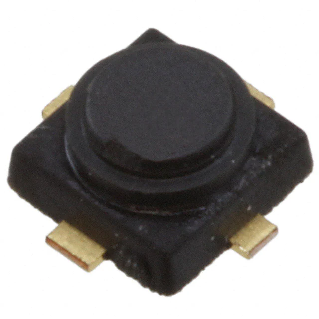
• Micro-X plastic (S02) package
APPLICATIONS
• X to Ku-band DBS LNB
• Other X to Ku-band communication systems
TI
ORDERING INFORMATION
Order Number
Package
NE3511S02-T1C
NE3511S02-T1C-A
S02 (Pb-Free)
NE3511S02-T1D
NE3511S02-T1D-A
Quantity
Marking
en
t:
Part Number
2 kpcs/reel
B
O
Re
p N
10 kpcs/reel
Supplying Form
• 8 mm wide embossed taping
• Pin 4 (Gate) faces the perforation side
of the tape
lac
em
Remark To order evaluation samples, contact your nearby sales office.
Part number for sample order: NE3511S02-A
ABSOLUTE MAXIMUM RATINGS (TA = +25°C)
Parameter
Symbol
Ratings
Unit
VDS
4
V
VGS
−3
V
Drain Current
ID
IDSS
mA
Gate Current
IG
100
µA
165
mW
Tch
+125
°C
Tstg
−65 to +125
°C
SC
Drain to Source Voltage
Gate to Source Voltage
Total Power Dissipation
In
Channel Temperature
D
D I
Storage Temperature
Ptot
Note
ro
p-
Note Mounted on 1.08 cm2 × 1.0 mm (t) glass epoxy PCB
Caution Observe precautions when handling because these devices are sensitive to electrostatic discharge.
Document No. PG10642EJ01V0DS (1st edition)
Date Published October 2006 NS CP(N)
�NE3511S02
RECOMMENDED OPERATING CONDITIONS (TA = +25°C)
Drain to Source Voltage
VDS
Drain Current
ID
Input Power
Pin
MIN.
TYP.
MAX.
Unit
1
2
3
V
5
10
20
mA
−
−
0
dBm
2
Symbol
NU
CE E
35
12 D
K
Parameter
ELECTRICAL CHARACTERISTICS (TA = +25°C, unless otherwise specified)
Parameter
Symbol
Gate to Source Leak Current
IGSO
Saturated Drain Current
IDSS
Gate to Source Cutoff Voltage
VGS (off)
gm
Noise Figure
NF
Associated Gain
Ga
MIN.
TYP.
MAX.
Unit
VGS = −3 V
−
0.5
10
µA
VDS = 2 V, VGS = 0 V
20
40
70
mA
VDS = 2 V, ID = 100 µA
−0.2
−0.7
−1.7
V
VDS = 2 V, ID = 10 mA
50
65
−
mS
VDS = 2 V, ID = 10 mA, f = 12 GHz
−
0.30
0.45
dB
12.5
13.5
−
dB
en
t:
lac
em
ro
p-
D
D I
In
SC
O
Re
p N
TI
Transconductance
Test Conditions
2
Data Sheet PG10642EJ01V0DS
�NE3511S02
TYPICAL CHARACTERISTICS (TA = +25°C, unless otherwise specified)
TOTAL POWER DISSIPATION
vs. AMBIENT TEMPERATURE
NU
CE E
35
12 D
K
100
250
200
150
100
50
2
Mounted on Glass Epoxy PCB
(1.08 cm2 × 1.0 mm (t) )
80
Drain Current ID (mA)
Total Power Dissipation Ptot (mW)
DRAIN CURRENT vs.
DRAIN TO SOURCE VOLTAGE
60
VGS = 0 V
40
–0.2 V
20
–0.4 V
–0.6 V
0
50
100
150
200
Ambient Temperature TA (˚C)
250
1.0
0
2.0
Drain to Source Voltage VDS (V)
80
60
20
0
–2.0
lac
em
40
O
Re
p N
Drain Current ID (mA)
VDS = 2 V
en
t:
TI
DRAIN CURRENT vs.
GATE TO SOURCE VOLTAGE
–1.0
0
MINIMUM NOISE FIGURE,
ASSOCIATED GAIN vs. FREQUENCY
1.4
Ga
1.2
0.8
0.6
0.4
0.2
ro
p-
1.0
2
4
6
NFmin
8
10
12
15
10
5
0.0
0
20
14
0
16 18 20
Minimum Noise Figure NFmin (dB)
In
1.6
25
VDS = 2 V
ID = 10 mA
Associated Gain Ga (dB)
1.8
D
D I
Minimum Noise Figure NFmin (dB)
2.0
MINIMUM NOISE FIGURE,
ASSOCIATED GAIN vs. DRAIN CURRENT
1.6
16
f = 12 GHz
1.4 VDS = 2 V
14
1.2
12
Ga
1.0
10
0.8
8
6
0.6
NFmin
0.4
4
Associated Gain Ga (dB)
SC
Gate to Source Voltage VGS (V)
2
0.2
0.0
0
Frequency f (GHz)
5
10
15
20
0
25
Drain Current ID (mA)
Remark The graphs indicate nominal characteristics.
Data Sheet PG10642EJ01V0DS
3
�NE3511S02
S-PARAMETERS
S-parameters/Noise parameters are provided on our web site in a form (S2P) that enables direct import to a
Click here to download S-parameters.
NU
CE E
35
12 D
K
microwave circuit simulator without keyboard input.
en
t:
lac
em
ro
p-
D
D I
In
SC
O
Re
p N
TI
URL http://www.ncsd.necel.com/microwave/index.html
4
Data Sheet PG10642EJ01V0DS
2
[RF and Microwave] → [Device Parameters]
�NE3511S02
RF MEASURING LAYOUT PATTERN (REFERENCE ONLY) (UNIT: mm)
NU
CE E
35
12 D
K
2.80
2.60
2
2.06
0.64
13.0
en
t:
TI
0.54
0.74
2.06
1.7 mm/R.P.
2.6
1.7
φ 0.3 TH
1.7
Reference Plane
(Calibration Plane)
lac
em
O
Re
p N
Reference Plane
(Calibration Plane)
6.0
RT/duroid 5880/ROGERS
t = 0.254 mm
εr = 2.20
tan delta = 0.0009 @10 GHz
ro
p-
D
D I
In
SC
L2–uX Ver. 1
Data Sheet PG10642EJ01V0DS
5
�NE3511S02
PACKAGE DIMENSIONS
NU
CE E
35
12 D
K
S02 (UNIT: mm)
(Bottom View)
2
(Top View)
3.2±0.2
0.65 TYP.
0.5 TYP.
B
2
2.2±0.2
1
1
2.6±0.1
2.2±0.2
4
4
2
3
3
2.2±0.2
lac
em
O
Re
p N
0.15±0.05
1.5 MAX.
1.7
en
t:
TI
(Side View)
PIN CONNECTIONS
1.
2.
3.
4.
Source
Drain
Source
Gate
ro
p-
D
D I
In
SC
3.2±0.2
6
Data Sheet PG10642EJ01V0DS
�NE3511S02
RECOMMENDED SOLDERING CONDITIONS
This product should be soldered and mounted under the following recommended conditions.
For soldering
Infrared Reflow
Partial Heating
Soldering Conditions
Condition Symbol
Peak temperature (package surface temperature)
: 260°C or below
Time at peak temperature
: 10 seconds or less
Time at temperature of 220°C or higher
: 60 seconds or less
Preheating time at 120 to 180°C
: 120±30 seconds
Maximum number of reflow processes
: 3 times
Maximum chlorine content of rosin flux (% mass)
: 0.2%(Wt.) or below
Peak temperature (terminal temperature)
: 350°C or below
Soldering time (per side of device)
: 3 seconds or less
Maximum chlorine content of rosin flux (% mass)
: 0.2%(Wt.) or below
IR260
2
Soldering Method
NU
CE E
35
12 D
K
methods and conditions other than those recommended below, contact your nearby sales office.
HS350
en
t:
lac
em
ro
p-
D
D I
In
SC
O
Re
p N
TI
Caution Do not use different soldering methods together (except for partial heating).
Data Sheet PG10642EJ01V0DS
7
�NE3511S02
GaAs Products
This product uses gallium arsenide (GaAs).
GaAs vapor and powder are hazardous to human health if inhaled or ingested, so please observe
the following points.
NU
CE E
35
12 D
K
Caution
• Follow related laws and ordinances when disposing of the product. If there are no applicable laws
and/or ordinances, dispose of the product as recommended below.
2
1. Commission a disposal company able to (with a license to) collect, transport and dispose of
materials that contain arsenic and other such industrial waste materials.
2. Exclude the product from general industrial waste and household garbage, and ensure that the
product is controlled (as industrial waste subject to special control) up until final disposal.
• Do not burn, destroy, cut, crush, or chemically dissolve the product.
ro
p-
D
D I
In
en
t:
lac
em
SC
O
Re
p N
TI
• Do not lick the product or in any way allow it to enter the mouth.
�2
I
en N
t:
U
CE E
35
12 D
K
4590 Patrick Henry Drive
Santa Clara, CA 95054-1817
Telephone: (408) 919-2500
Facsimile: (408) 988-0279
Subject: Compliance with EU Directives
CEL certifies, to its knowledge, that semiconductor and laser products detailed below are compliant
with the requirements of European Union (EU) Directive 2002/95/EC Restriction on Use of Hazardous
Substances in electrical and electronic equipment (RoHS) and the requirements of EU Directive
2003/11/EC Restriction on Penta and Octa BDE.
CEL Pb-free products have the same base part number with a suffix added. The suffix –A indicates
that the device is Pb-free. The –AZ suffix is used to designate devices containing Pb which are
exempted from the requirement of RoHS directive (*). In all cases the devices have Pb-free terminals.
All devices with these suffixes meet the requirements of the RoHS directive.
O
Re
pla N
c T
This status is based on CEL’s understanding of the EU Directives and knowledge of the materials that
go into its products as of the date of disclosure of this information.
Lead (Pb)
Mercury
Concentration Limit per RoHS
(values are not yet fixed)
em
Restricted Substance
per RoHS
< 1000 PPM
Concentration contained
in CEL devices
-A
Not Detected
< 1000 PPM
Not Detected
< 100 PPM
Not Detected
Hexavalent Chromium
< 1000 PPM
Not Detected
PBB
< 1000 PPM
Not Detected
< 1000 PPM
Not Detected
SC
Cadmium
PBDE
-AZ
(*)
-In
If you should have any additional questions regarding our devices and compliance to environmental
standards, please do not hesitate to contact your local representative.
ro
p
D
D I
Important Information and Disclaimer: Information provided by CEL on its website or in other communications concerting the substance
content of its products represents knowledge and belief as of the date that it is provided. CEL bases its knowledge and belief on information
provided by third parties and makes no representation or warranty as to the accuracy of such information. Efforts are underway to better
integrate information from third parties. CEL has taken and continues to take reasonable steps to provide representative and accurate
information but may not have conducted destructive testing or chemical analysis on incoming materials and chemicals. CEL and CEL
suppliers consider certain information to be proprietary, and thus CAS numbers and other limited information may not be available for
release.
In no event shall CEL’s liability arising out of such information exceed the total purchase price of the CEL part(s) at issue sold by CEL to
customer on an annual basis.
See CEL Terms and Conditions for additional clarification of warranties and liability.
�NOTICE
4.
5.
6.
7.
8.
9.
2
SC
10.
I
en N
t:
U
CE E
35
12 D
K
3.
em
2.
Descriptions of circuits, software and other related information in this document are provided only to illustrate the operation of semiconductor products and
application examples. You are fully responsible for the incorporation of these circuits, software, and information in the design of your equipment. California
Eastern Laboratories and Renesas Electronics assumes no responsibility for any losses incurred by you or third parties arising from the use of these circuits,
software, or information.
California Eastern Laboratories has used reasonable care in preparing the information included in this document, but California Eastern Laboratories does
not warrant that such information is error free. California Eastern Laboratories and Renesas Electronics assumes no liability whatsoever for any damages
incurred by you resulting from errors in or omissions from the information included herein.
California Eastern Laboratories and Renesas Electronics do not assume any liability for infringement of patents, copyrights, or other intellectual property
rights of third parties by or arising from the use of Renesas Electronics products or technical information described in this document. No license, express,
implied or otherwise, is granted hereby under any patents, copyrights or other intellectual property rights of California Eastern Laboratories or Renesas
Electronics or others.
You should not alter, modify, copy, or otherwise misappropriate any Renesas Electronics product, whether in whole or in part. California Eastern
Laboratories and Renesas Electronics assume no responsibility for any losses incurred by you or third parties arising from such alteration, modification, copy
or otherwise misappropriation of Renesas Electronics product.
Renesas Electronics products are classified according to the following two quality grades: “Standard” and “High Quality”. The recommended applications
for each Renesas Electronics product depends on the product’s quality grade, as indicated below. “Standard”: Computers; office equipment; communications
equipment; test and measurement equipment; audio and visual equipment; home electronic appliances; machine tools; personal electronic equipment; and
industrial robots etc. “High Quality”: Transportation equipment (automobiles, trains, ships, etc.); traffic control systems; anti-disaster systems; anti-crime
systems; and safety equipment etc. Renesas Electronics products are neither intended nor authorized for use in products or systems that may pose a direct
threat to human life or bodily injury (artificial life support devices or systems, surgical implantations etc.), or may cause serious property damages (nuclear
reactor control systems, military equipment etc.). You must check the quality grade of each Renesas Electronics product before using it in a particular
application. You may not use any Renesas Electronics product for any application for which it is not intended. California Eastern Laboratories and Renesas
Electronics shall not be in any way liable for any damages or losses incurred by you or third parties arising from the use of any Renesas Electronics product
for which the product is not intended by California Eastern Laboratories or Renesas Electronics.
You should use the Renesas Electronics products described in this document within the range specified by California Eastern Laboratories, especially with
respect to the maximum rating, operating supply voltage range, movement power voltage range, heat radiation characteristics, installation and other product
characteristics. California Eastern Laboratories shall have no liability for malfunctions or damages arising out of the use of Renesas Electronics products
beyond such specified ranges.
Although Renesas Electronics endeavors to improve the quality and reliability of its products, semiconductor products have specific characteristics such as
the occurrence of failure at a certain rate and malfunctions under certain use conditions. Further, Renesas Electronics products are not subject to radiation
resistance design. Please be sure to implement safety measures to guard them against the possibility of physical injury, and injury or damage caused by
fire in the event of the failure of a Renesas Electronics product, such as safety design for hardware and software including but not limited to redundancy,
fire control and malfunction prevention, appropriate treatment for aging degradation or any other appropriate measures. Because the evaluation of
microcomputer software alone is very difficult, please evaluate the safety of the final products or systems manufactured by you.
Please contact a California Eastern Laboratories sales office for details as to environmental matters such as the environmental compatibility of each Renesas
Electronics product. Please use Renesas Electronics products in compliance with all applicable laws and regulations that regulate the inclusion or use of
controlled substances, including without limitation, the EU RoHS Directive. California Eastern Laboratories and Renesas Electronics assume no liability for
damages or losses occurring as a result of your noncompliance with applicable laws and regulations.
Renesas Electronics products and technology may not be used for or incorporated into any products or systems whose manufacture, use, or sale is prohibited
under any applicable domestic or foreign laws or regulations. You should not use Renesas Electronics products or technology described in this document
for any purpose relating to military applications or use by the military, including but not limited to the development of weapons of mass destruction. When
exporting the Renesas Electronics products or technology described in this document, you should comply with the applicable export control laws and
regulations and follow the procedures required by such laws and regulations.
It is the responsibility of the buyer or distributor of California Eastern Laboratories, who distributes, disposes of, or otherwise places the Renesas Electronics
product with a third party, to notify such third party in advance of the contents and conditions set forth in this document, California Eastern Laboratories and
Renesas Electronics assume no responsibility for any losses incurred by you or third parties as a result of unauthorized use of Renesas Electronics products.
This document may not be reproduced or duplicated in any form, in whole or in part, without prior written consent of California Eastern Laboratories.
Please contact a California Eastern Laboratories sales office if you have any questions regarding the information contained in this document or Renesas
Electronics products, or if you have any other inquiries.
O
Re
pla N
c T
1.
11.
12.
D
D I
-In
NOTE 1: “Renesas Electronics” as used in this document means Renesas Electronics Corporation and also includes its majority-owned subsidiaries.
NOTE 2: “Renesas Electronics product(s)” means any product developed or manufactured by or for Renesas Electronics.
NOTE 3: Products and product information are subject to change without notice.
ro
p
CEL Headquarters • 4590 Patrick Henry Drive, Santa Clara, CA 95054 • Phone (408) 919-2500 • www.cel.com
For a complete list of sales offices, representatives and distributors,
Please visit our website: www.cel.com/contactus
�