NPN EPITAXIAL SILICON
TRANSISTOR HIGH FREQUENCY
LOW DISTORTION AMPLIFIER
FEATURES
•
•
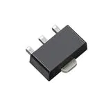
PACKAGE OUTLINE M02
HIGH COLLECTOR CURRENT:
250 mA MAX
NEW HIGH GAIN POWER MINI-MOLD PACKAGE
(SOT-89 TYPE)
HIGH OUTPUT POWER AT 1 dB COMPRESSION:
27 dBm TYP at 1 GHz
HIGH IP3:
37 dBm TYP at 1 GHz
BOTTOM VIEW
4.5±0.1
1.6±0.2
1.5±0.1
C
DESCRIPTION
NEC's NE461M02 is an NPN silicon epitaxial bipolar transistor
designed for medium power applications requiring high dynamic range and low intermodulation distortion. This device
offers excellent performance and reliability at low cost through
NEC's titanium, platinum, gold metallization system and direct
nitride passivation of the surface of the chip. The NE461M02
is an excellent choice for low noise amplifiers in the VHF to UHF
band and is suitable for CATV and other telecommunication
applications.
B
E
0.8
MIN
E
3.95±0.26
•
OUTLINE DIMENSIONS (Units in mm)
2.45±0.1
•
NE461M02
0.42
±0.06
0.42
±0.06
0.25±0.02
0.45
±0.06
1.5
3.0
PIN CONNECTIONS
E: Emitter
C: Collector
B: Base
ELECTRICAL CHARACTERISTICS (TA = 25°C)
PART NUMBER
EIAJ1 REGISTERED NUMBER
PACKAGE OUTLINE
SYMBOLS
NE461M02
2SC5337
M02
TYP
MAX
ICBO
Collector Cutoff Current at VCB = 20 V, IE = 0
µA
0.01
5.0
IEBO
Emitter Cutoff Current at VEB = 2 V, IC = 0
µA
0.03
5.0
hFE2
DC Current Gain at VCE = 10 V, IC = 50 mA
40
120
200
7.0
8.3
|S21E|2
NF1
PARAMETERS AND CONDITIONS
UNITS
Insertion Power Gain at VCE = 10 V, IC = 50 mA, f = 1 GHz
dB
Noise Figure 1 at VCE = 10 V, IC = 50 mA, f = 500 MHz3
dB
MIN
1.5
3.5
dB
2.0
3.5
dB
59.0
NF2
Noise Figure 2 at VCE = 10 V, IC = 50 mA, f = 1
IM2
2nd Order Intermodulation Distortion
VCE = 10 V, IC = 50 mA, Rs = RL = 75 Ω
Pin = 105 dB µV/75 Ω, f1 = 190 MHz
f2 = 90 MHz, f = f1 - f2
IM3
3rd Order Intermodulation Distortion
VCE = 10 V, IC = 50 mA, Rs = RL = 75 Ω
Pin = 105 dB µV/75 Ω, f1 = 190 MHz
f2 = 200 MHz, f = 2 x f1 - f2
dB
82.0
GHz3
Notes:
1. Electronic Industrial Association of Japan.
2. Pulsed measurement, pulse width ≤ 350 µs, duty cycle ≤ 2 %.
3. Rs = RL = 50 Ω, tuned.
California Eastern Laboratories
�NE461M02
ABSOLUTE MAXIMUM RATINGS1 (TA = 25°C)
SYMBOLS
PARAMETERS
UNITS
RATINGS
VCBO
Collector to Base Voltage
V
30
VCEO
Collector to Emitter Voltage
V
15
VEBO
Emitter to Base Voltage
V
3.0
mA
250
IC
Collector Current
PT
Total Power Dissipation2
W
2.0
TJ
Junction Temperature
°C
150
TSTG
Storage Temperature
°C
-65 to +150
ORDERING INFORMATION
PART NUMBER
NE461M02-T1-AZ
QUANTITY
PACKAGING
1000
Tape & Reel
Notes:
1. Operation in excess of any one of these parameters may result
in permanent damage.
2. Device mounted on 0.7 mm x 16 cm2 double-sided ceramic
substrate (copper plating).
TYPICAL PERFORMANCE CURVES (TA = 25°C)
DC CURRENT GAIN VS.
COLLECTOR CURRENT
COLLECTOR CURRENT VS.
COLLECTOR TO EMITTER VOLTAGE
300
0.5 mA
80
DC Current Gain, hFE
Collector Current, IC (mA)
VCE 10 V
IB=0.6 mA
100
0.4 mA
60
0.3 mA
40
0.2 mA
100
50
20
0.1 mA
10
10
0
0.1
20
Collector to Emitter Voltage, VCE (V)
10
100
1000
Collector Current, Ic (mA)
FEEDBACK CAPACITANCE vs.
COLLECTOR TO BASE VOLTAGE
GAIN BANDWIDTH PRODUCT vs.
COLLECTOR CURRENT
10
5.0
VCE = 10 V
f = 1 GHz
5
3
2
1
0.5
0.3
10
30
50
70
100
Collector Current, Ic (mA)
f = 1.0 MHz
Feedback Capacitance, CrE (pF)
Gain Bandwidth Product, fT (GHz)
1
3.0
2.0
1.0
0.5
0.3
1
3
5
10
20
Collector to Base Voltage, VCB (V)
30
�NE461M02
TYPICAL PERFORMANCE CURVES (TA = 25°C)
INSERTION POWER GAIN and MAXIMUM
AVAILABLE GAIN vs. FREQUENCY
10
5
0
10
30
50
|S21E|
Maximum Available Gain, MAG (dB)
VCE = 10 V
f = 1 GHz
Insertion Power Gain, IS21E|2 (dB)
Insertion Power Gain, IS21E|2 (dB)
INSERTION POWER GAIN vs.
COLLECTOR CURRENT
MAG
20
10
VCE = 10 V
IC = 50 MA
0
70 100
0.2
VCE = 10 V
f = 1 GHz
Noise Figure, NF (dB)
6
5
4
3
2
1
0
5
10
20
50
100
Collector Current, Ic (mA)
0.6 0.8 1.0
1.4
2.0
3RD ORDER INTERMODULATION DISTORTION
2ND ORDER INTERMODULATION DISTORTION (+) &
2ND ORDER INTERMODULATION DISTORTION (-) vs.
COLLECTOR CURRENT
3rd Order Intermodulation Distortion, IM3 (dBc)
2nd Order Intermodulation Distortion, IM2+ (dBc)
2nd Order Intermodulation Distortion,IM2- (dBc)
7
0.4
Frequency, f (GHz)
Collector Current, Ic (mA)
NOISE FIGURE vs.
COLLECTOR CURRENT
2
80
IM3
70
60
IM2+
IM250
40
VCE=10 V
30
10
IM3: Vo = 110 dB µV/75 Ω 2 tone each
f = 2 x 190 MHz - 200 Mhz
IM2+: Vo = 105 dB µV/75 Ω 2 tone each
f = 90 MHz + 100 MHz
IM2-: Vo 105 dB µV/75 Ω 2 tone each
f = 190 MHz - 90 MHz
50
100
Collector Current, IC (mA)
300
�NE461M02
TYPICAL SCATTERING PARAMETERS (TA = 25°C)
j50
90˚
120˚
j100
j25
60˚
S21
0.1 GHz
150˚
30˚
j10
S22
3 GHz
0
S11
3 GHz
S21
3 GHz
180˚
0
S12
0.1 GHz
-j10
S11
0.1 GHz
S22
0.1 GHz
Coordinates in Ohms
Frequency in GHz
VCE = 10 V, IC = 50 mA
-j100
-j25
NE461M02
VCE = 5 V, IC = 50 mA
FREQUENCY
-150˚
-120˚
S11
S21
GHz
MAG
ANG
0.603
0.615
0.618
0.616
0.612
0.607
0.602
0.596
0.588
0.581
0.572
0.563
0.553
0.544
0.535
0.527
-142.0
-165.0
178.5
168.9
161.2
154.4
148.0
142.0
136.2
130.6
125.0
119.6
114.0
108.4
102.7
97.0
-30˚
-60˚
-90˚
-j50
0.100
0.200
0.400
0.600
0.800
1.000
1.200
1.400
1.600
1.800
2.000
2.200
2.400
2.600
2.800
3.000
0˚
S12
3 GHz
S12
S22
MAG
ANG
MAG
ANG
MAG
22.351
11.847
6.043
4.072
3.089
2.506
2.123
1.858
1.661
1.514
1.397
1.307
1.232
1.169
1.118
1.074
109.2
95.2
83.2
75.1
68.2
61.8
55.8
50.2
44.9
39.8
35.1
30.3
25.9
21.6
17.5
13.4
0.031
0.042
0.066
0.092
0.119
0.146
0.172
0.198
0.224
0.250
0.275
0.300
0.325
0.349
0.373
0.396
47.3
52.4
60.8
63.4
63.4
62.2
60.4
58.2
55.9
53.3
50.6
47.8
44.9
41.9
38.8
35.6
0.456
0.345
0.309
0.307
0.310
0.315
0.321
0.328
0.335
0.341
0.347
0.353
0.359
0.363
0.369
0.373
K
ANG
-100.7
-129.0
-147.0
-152.1
-153.5
-153.6
-153.3
-152.8
-152.2
-151.7
-151.5
-151.4
-151.4
-151.8
-152.4
-153.3
MAG1
(dB)
0.50
0.77
0.97
1.04
1.06
1.07
1.07
1.06
1.06
1.05
1.04
1.03
1.02
1.01
1.00
1.00
28.6
24.5
19.6
15.3
12.7
10.8
9.3
8.2
7.3
6.5
5.9
5.4
5.0
4.6
4.5
4.3
VCE = 10 V, IC = 50 mA
FREQUENCY
S11
S21
GHz
MAG
ANG
0.100
0.200
0.400
0.600
0.800
1.000
1.200
1.400
1.600
1.800
2.000
2.200
2.400
2.600
2.800
3.000
0.599
0.602
0.601
0.599
0.596
0.591
0.586
0.581
0.573
0.566
0.557
0.549
0.540
0.531
0.523
0.515
-137.2
-162.2
179.8
169.8
161.9
155.0
148.5
142.4
136.6
131.0
125.5
120.1
114.5
108.9
103.2
97.5
S12
S22
MAG
ANG
MAG
ANG
MAG
23.210
12.353
6.307
4.248
3.220
2.609
2.208
1.929
1.722
1.568
1.444
1.349
1.269
1.202
1.148
1.101
109.9
95.7
83.5
75.4
68.4
62.1
56.1
50.5
45.2
40.1
35.3
30.5
26.1
21.8
17.6
13.5
0.031
0.042
0.066
0.091
0.117
0.144
0.169
0.195
0.220
0.245
0.270
0.295
0.319
0.342
0.366
0.388
48.0
51.4
60.0
62.8
63.0
61.9
60.2
58.1
55.8
53.3
50.7
48.0
45.1
42.2
39.1
36.0
0.455
0.335
0.295
0.292
0.295
0.301
0.309
0.317
0.325
0.333
0.340
0.347
0.354
0.360
0.366
0.372
K
ANG
-97.0
-125.3
-143.9
-149.2
-150.6
-150.7
-150.3
-149.7
-149.1
-148.6
-148.3
-148.2
-148.2
-148.6
-149.2
-150.1
MAG1
(dB)
0.48
0.75
0.97
1.03
1.06
1.07
1.07
1.06
1.06
1.05
1.04
1.03
1.02
1.01
1.00
0.99
28.7
24.7
19.8
15.6
12.9
11.0
9.6
8.4
7.5
6.7
6.1
5.6
5.2
4.8
4.8
4.5
Note:
1. Gain Calculations:
MAG =
|S21|
|S12|
(K ±
K 2- 1
). When K ≤ 1, MAG is undefined and MSG values are used. MSG =
MAG = Maximum Available Gain
MSG = Maximum Stable Gain
2
2
2
|S21|
, K = 1 + | ∆ | - |S11| - |S22| , ∆ = S11 S22 - S21 S12
|S12|
2 |S12 S21|
�NE461M02
TYPICAL SCATTERING PARAMETERS (TA = 25°C)
j50
90˚
120˚
j100
j25
60˚
S21
0.1 GHz
150˚
30˚
j10
S22
3 GHz
S11
3 GHz
0
180˚
0
S11
0.1 GHz
-j10
S22
0.1 GHz
Coordinates in Ohms
Frequency in GHz
VCE = 12 V, IC = 100 mA
-j100
-j25
NE461M02
VCE = 10 V, IC = 100 mA
FREQUENCY
0˚
S21
3 GHz
-150˚
S21
MAG
ANG
0.596
0.601
0.601
0.600
0.597
0.593
0.588
0.581
0.574
0.565
0.556
0.547
0.535
0.524
0.515
0.505
-144.8
-166.5
177.5
168.1
160.4
153.6
147.2
141.2
135.3
129.6
124.1
118.7
113.0
107.5
101.8
96.1
-30˚
-60˚
-90˚
S11
GHz
S12
3 GHz
-120˚
-j50
0.100
0.200
0.400
0.600
0.800
1.000
1.200
1.400
1.600
1.800
2.000
2.200
2.400
2.600
2.800
3.000
S12
0.1 GHz
S12
S22
MAG
ANG
MAG
ANG
MAG
23.959
12.575
6.386
4.296
3.258
2.640
2.236
1.953
1.747
1.590
1.468
1.371
1.292
1.225
1.170
1.122
106.7
93.9
82.7
75.0
68.3
62.1
56.3
50.8
45.6
40.6
35.8
31.1
26.6
22.3
18.1
14.1
0.029
0.040
0.066
0.093
0.120
0.147
0.174
0.201
0.227
0.252
0.277
0.302
0.325
0.348
0.371
0.393
48.5
55.6
63.6
65.3
64.7
63.1
60.9
58.5
55.9
53.1
50.3
47.4
44.3
41.3
38.2
35.1
0.422
0.334
0.308
0.306
0.309
0.313
0.318
0.324
0.330
0.335
0.341
0.346
0.351
0.355
0.359
0.363
K
ANG
-108.4
-135.7
-152.0
-156.5
-157.7
-157.8
-157.4
-156.6
-155.7
-154.9
-154.2
-153.5
-153.0
-152.8
-152.8
-153.0
MAG1
(dB)
0.56
0.82
0.99
1.04
1.06
1.06
1.06
1.06
1.05
1.05
1.04
1.03
1.02
1.02
1.01
1.00
29.2
25.0
19.9
15.4
12.9
11.0
9.5
8.4
7.5
6.7
6.1
5.5
5.1
4.7
4.4
4.2
VCE = 12 V, IC = 100 mA
FREQUENCY
GHz
0.100
0.200
0.400
0.600
0.800
1.000
1.200
1.400
1.600
1.800
2.000
2.200
2.400
2.600
2.800
3.000
S11
MAG
0.596
0.598
0.597
0.595
0.592
0.588
0.583
0.576
0.568
0.560
0.550
0.540
0.530
0.520
0.510
0.502
S21
ANG
-143.1
-165.5
178.0
168.4
160.6
153.7
147.3
141.3
135.5
129.9
124.4
119.0
113.5
107.9
102.3
96.7
MAG
24.061
12.640
6.417
4.313
3.268
2.647
2.241
1.957
1.750
1.593
1.471
1.373
1.294
1.228
1.172
1.123
S12
ANG
106.9
94.0
82.7
74.9
68.2
62.0
56.2
50.7
45.5
40.5
35.6
31.0
26.4
22.1
17.9
13.8
MAG
0.029
0.040
0.065
0.093
0.120
0.147
0.173
0.199
0.225
0.250
0.275
0.300
0.323
0.346
0.369
0.391
K
MAG1
0.56
0.82
0.99
1.04
1.06
1.07
1.07
1.07
1.06
1.05
1.04
1.03
1.03
1.02
1.01
1.01
(dB)
29.3
25.0
19.9
15.4
12.8
11.0
9.5
8.3
7.4
6.6
6.0
5.5
5.0
4.6
4.4
4.1
S22
ANG
48.3
55.1
63.0
64.8
64.3
62.8
60.7
58.3
55.8
53.1
50.2
47.4
44.3
41.3
38.2
35.0
MAG
0.416
0.328
0.301
0.299
0.302
0.306
0.312
0.318
0.324
0.330
0.336
0.342
0.347
0.353
0.357
0.362
ANG
-107.7
-135.1
-151.6
-156.2
-157.4
-157.4
-156.9
-156.1
-155.2
-154.3
-153.5
-152.8
-152.3
-152.0
-151.9
-152.2
Note:
1. Gain Calculations:
MAG =
|S21|
|S12|
(K ±
K 2- 1
). When K ≤ 1, MAG is undefined and MSG values are used. MSG =
2
2
2
|S21|
, K = 1 + | ∆ | - |S11| - |S22| , ∆ = S11 S22 - S21 S12
|S12|
2 |S12 S21|
MAG = Maximum Available Gain
MSG = Maximum Stable Gain
Life Support Applications
These NEC products are not intended for use in life support devices, appliances, or systems where the malfunction of these products can reasonably
be expected to result in personal injury. The customers of CEL using or selling these products for use in such applications do so at their own risk and
agree to fully indemnify CEL for all damages resulting from such improper use or sale.
EXCLUSIVE NORTH AMERICAN AGENT FOR
RF, MICROWAVE & OPTOELECTRONIC SEMICONDUCTORS
CALIFORNIA EASTERN LABORATORIES • Headquarters • 4590 Patrick Henry Drive • Santa Clara, CA 95054-1817 • (408) 988-3500 • Telex 34-6393 • FAX (408) 988-0279
24-Hour Fax-On-Demand: 800-390-3232 (U.S. and Canada only) • Internet: http://WWW.CEL.COM
PRINTED IN USA ON RECYCLED PAPER -12/98
DATA SUBJECT TO CHANGE WITHOUT NOTICE
�4590 Patrick Henry Drive
Santa Clara, CA 95054-1817
Telephone: (408) 919-2500
Facsimile: (408) 988-0279
Subject: Compliance with EU Directives
CEL certifies, to its knowledge, that semiconductor and laser products detailed below are compliant
with the requirements of European Union (EU) Directive 2002/95/EC Restriction on Use of Hazardous
Substances in electrical and electronic equipment (RoHS) and the requirements of EU Directive
2003/11/EC Restriction on Penta and Octa BDE.
CEL Pb-free products have the same base part number with a suffix added. The suffix –A indicates
that the device is Pb-free. The –AZ suffix is used to designate devices containing Pb which are
exempted from the requirement of RoHS directive (*). In all cases the devices have Pb-free terminals.
All devices with these suffixes meet the requirements of the RoHS directive.
This status is based on CEL’s understanding of the EU Directives and knowledge of the materials that
go into its products as of the date of disclosure of this information.
Restricted Substance
per RoHS
Concentration Limit per RoHS
(values are not yet fixed)
Concentration contained
in CEL devices
-A
Not Detected
Lead (Pb)
< 1000 PPM
Mercury
< 1000 PPM
Not Detected
Cadmium
< 100 PPM
Not Detected
Hexavalent Chromium
< 1000 PPM
Not Detected
PBB
< 1000 PPM
Not Detected
PBDE
< 1000 PPM
Not Detected
-AZ
(*)
If you should have any additional questions regarding our devices and compliance to environmental
standards, please do not hesitate to contact your local representative.
Important Information and Disclaimer: Information provided by CEL on its website or in other communications concerting the substance
content of its products represents knowledge and belief as of the date that it is provided. CEL bases its knowledge and belief on information
provided by third parties and makes no representation or warranty as to the accuracy of such information. Efforts are underway to better
integrate information from third parties. CEL has taken and continues to take reasonable steps to provide representative and accurate
information but may not have conducted destructive testing or chemical analysis on incoming materials and chemicals. CEL and CEL
suppliers consider certain information to be proprietary, and thus CAS numbers and other limited information may not be available for
release.
In no event shall CEL’s liability arising out of such information exceed the total purchase price of the CEL part(s) at issue sold by CEL to
customer on an annual basis.
See CEL Terms and Conditions for additional clarification of warranties and liability.
�