DATA SHEET
SHEET
DATA
SILICON TRANSISTOR
NE68033 / 2SC3585
JEITA
Part No.
+0.1
0.4 −0.05
2
1
3
ABSOLUTE MAXIMUM RATINGS (TA = 25 �C)
Marking
+0.1
0.16 −0.06
V
V
V
mA
mW
�C
�C
0.3
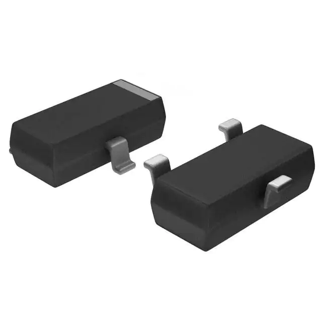
PIN CONNECTIONS
1. Emitter
2. Base
3. Collector
0 to 0.1
20
10
1.5
35
200
150
�65 to +150
1.1 to 1.4
VCBO
VCEO
VEBO
IC
PT
Tj
Tstg
PH
AS
Collector to Base Voltage
Collector to Emitter Voltage
Emitter to Base Voltage
Collector Current
Total Power Dissipation
Junction Temperature
Storage Temperature
0.65 −0.15
+0.1
@f = 2.0 GHz
@f = 2.0 GHz
+0.1
1.5
0.4 −0.05
1.8 dB TYP.
9 dB TYP.
E-
• NF
• Ga
2.8±0.2
0.95
FEATURES
PACKAGE DIMENSIONS
(Units: mm)
0.95
The NE68033 / 2SC3585 is an NPN epitaxial silicon transistor designed
for use in low-noise and small signal amplifiers from VHF band to UHF
band. The NE68033 / 2SC3585 features excellent power gain with very
low-noise figures.
The NE68033 / 2SC3585 employs direct nitride
passivated base surface process (DNP process) which is a proprietary
new fabrication technique which provides excellent noise figures at
high current values. This allows excellent associated gain and very
wide dynamic range.
2.9±0.2
DESCRIPTION
O
UT
MICROWAVE LOW NOISE AMPLIFIER
NPN SILICON EPITAXIAL TRANSISOR
ELECTRICAL CHARACTERISTICS (TA = 25 �C)
CHARACTERISTIC
SYMBOL
MIN.
TYP.
MAX.
UNIT
TEST CONDITIONS
Collector Cutoff Current
ICBO
1.0
�A
VCB = 10 V, IE = 0
Emitter Cutoff Current
IEBO
1.0
�A
VEB = 1 V, IC = 0
DC Current Gain
hFE *
Gain Bandwidth Product
fT
Feed-Back Capacitance
Cre **
Maximum Available Gain
100
250
10
GHz
8.0
dB
VCE = 6 V, IC = 10 mA, f = 2.0 GHz
MAG
10
dB
VCE = 6 V, IC = 10 mA, f = 2.0 GHz
NF
1.8
dB
VCE = 6 V, IC = 5 mA, f = 2.0 GHz
2
6.0
0.8
VCE = 6 V, IC = 10 mA
VCB = 10 V, IE = 0, f = 1.0 MHz
Noise Figure
0.3
VCE = 6 V, IC = 10 mA
pF
�S21e�
Insertion Power Gain
50
3.0
* Pulse Measurement PW � 350 �s, Duty Cycle � 2 %
** The emitter terminal and the case shall be connected to the gurad terminal of the three-terminal capacitance bridge.
hFE Classification
Class
R43/Q *
R44/R *
R45/S *
Marking
R43
R44
R45
hFE
50 to 100
80 to 160
125 to 250
* Old Specification / New Specification
Document No. P10361EJ4V1DS00 (4th edition)
Date Published March 1997 N
�NE68033 / 2SC3585
TYPICAL CHARACTERISTICS (TA = 25 C)
3
Free Air
200
100
50
0
100
150
TA-Ambient Temperature-°C
50
PH
AS
20
1
5
10
50
IC-Collector Current-mA
VCE = 6 V
20
10
7
5
3
2
1
2
GAIN BANDWIDTH PRODUCT vs.
COLLECTOR CURRENT
MAG-Maximum Available Gain-dB
|S21e|2-Insertion Gain -dB
fT-Gain Bandwidth Product-MHz
30
0.7
0.5
0.3
0.2
2
3
5
7
10
VCB-Collector to Base Voltage-V
20
30
20
30
INSERTION GAIN vs.
COLLECTOR CURRENT
VCE = 6 V
f = 2.0 GHz
E-
100
10
0.5
1
10
VCE = 6 V
|S21e|2-Insertion Gain-dB
hFE-DC Current Gain
200
f = 1.0 MHz
2
0.1
1
DC CURRENT GAIN vs.
COLLECTOR CURRENT
FEED-BACK CAPACITANCE vs.
COLLECTOR TO BASE VOLTAGE
O
UT
Cre-Feed-back Capacitance-pF
PT-Total Power Dissipation-W
TOTAL POWER DISSIPATION vs.
AMBIENT TEMPERATURE
2
3
5
7
10
IC-Collector Current-mA
20
30
8
6
4
2
0
1
20
16
2
3
5
7
10
IC-Collector Current-mA
INSERTION GAIN, MAXIMUM AVAILABLE
GAIN vs. FREQUENCY
VCE = 6 V
IC = 10 mA
MAG
|S21e|
2
12
8
4
0
0.1
0.2
0.3
0.5 7.0 1.0
f-Frequency-GHz
2.0 3.0
�NE68033 / 2SC3585
NOISE FIGURE vs.
COLLECTOR CURRENT
7
VCE = 6 V
f = 2.0 GHz
5
4
3
2
1
0
0.5
1
O
UT
NF-Noise Figure-dB
6
5
10
50 70
IC-Collector Current-mA
S-PARAMETER
VCE = 6.0 V, IC = 3.0 mA, ZO = 50
S11
S11
S21
S12
S12
S22
S22
200
0.858
23.1
8.499
153.3
0.030
46.5
0.905
13.5
400
0.724
40.6
6.923
131.6
0.060
58.7
0.826
21.2
600
0.580
51.1
5.951
118.4
0.080
60.3
0.749
27.0
800
0.457
58.9
4.615
104.9
0.099
60.2
0.666
28.6
1000
0.362
65.6
4.134
98.0
0.106
61.2
0.614
30.1
1200
0.304
73.1
3.412
88.9
0.129
61.1
0.574
30.0
1400
0.232
82.2
3.180
82.0
0.148
60.1
0.542
31.7
1600
0.179
84.9
2.763
75.7
0.154
59.5
0.514
35.2
1800
0.147
88.2
2.726
70.5
0.188
58.7
0.483
40.1
2000
0.108
104.1
2.378
64.9
0.197
56.8
0.455
42.6
S21
S21
S12
S12
S22
S22
E-
S21
PH
AS
f (MHz)
VCE = 6.0 V, IC = 10.0 mA, ZO = 50
f (MHz)
S11
S11
200
0.613
37.0
16.141
133.9
0.021
52.5
0.781
19.4
400
0.406
53.6
10.096
111.5
0.053
70.6
0.651
22.4
600
0.285
56.0
7.640
101.4
0.064
73.0
0.590
24.0
800
0.214
57.6
5.564
90.7
0.089
71.7
0.548
22.8
1000
0.156
58.1
4.787
86.0
0.095
70.6
0.526
23.3
1200
0.130
54.2
3.876
79.3
0.119
70.3
0.506
22.1
1400
0.105
56.5
3.573
74.0
0.141
68.3
0.489
24.8
1600
0.065
55.0
3.058
69.4
0.158
68.9
0.470
27.9
1800
0.042
48.9
2.997
65.3
0.178
66.5
0.439
31.4
2000
0.018
65.6
2.590
60.7
0.202
66.2
0.426
36.5
3
�NE68030 / 2SC3585
S-PARAMETER
1.4
1.2
1.0
0.9
1.6
0.7
1.8
2.0
5
O
UT
N
4
0.
O
4.0
1.0
0
1.
6.0
0.6
0.4
5.0
20
10
4.0
1.6
1.4
1.2
0.9
1.0
0.7
0.8
0.6
0.5
0.4
3.0
S22e 0.2 GHz
10
0.1
0.3
1.8
2.0
z
GH
0.27
0.23
IC = 3 mA
0.6
0
1.
5.0
0.8
(
E
NC
TA X
AC −J––O–
RE
–Z
0
3.
0.6
E
IV
AT
4.0
)
1.0
0.2 GHz
S11e
0
NE
G
2.0
1.8
0.35
0.15
−70
0.36
0.14
−80
−90
0.37
0.13
0.38
0.12
0.
4
0. 3
07
30
−1
0.39
0.11
−100
0
−11
0.40
0.10
0.4
0.0 2
8
0
−1
2
0.4
1
0.0
9
E-
4
0.3
6
0.1
1.4
1.6
0.2
1.2
0
1.0
3
0.3 7
−6
0.9
0.1
0.8
18
0
0.7
32
−5
0.6
0.
0.
5
0.4
0.
0. 31
19
0.
0.2
8
0.2
2
−20
8
0.
−4
4
−10
2.0
0.4
50
)
50
0.26
0.24
IC = 10 mA
0. 25
0.25
0.2
20
S22e
20
0.3
0.2
0.8
10
2.0 GHz
0
(
0.24
0.23
0.26
2
0.2
0.27
8
10
0.2
20
( –Z–+–J–XTANCE CO
) MPO
0
3.
0.8
0
.
2
9
0.2
1
0.3
−3
0.2 0
0
0
120°
S12e-FREQUENCY
CONDITION
PH
AS
IC = 10 mA
30°
S21e
60°
2.0 GHz
IC = 10 mA
150°
30°
S12e
IC = 3 mA
1.0 GHz
2.0 GHz
0.2 GHz 1.0 GHz
2.0 GHz
0
4
8
12
16
0° 180°
20
−30°
−60°
−120°
−90°
VCE = 6 V
90°
120°
60°
−150°
4
0.
18
32
0.
50
0.6
VCE = 6 V
90°
180°
0.1
0.3 7
3
600
1
0.2
9
0.2
30
S21e-FREQUENCY CONDITION
IC = 3 mA
0.1
6
0.3
4
0.4
REACTANCE COMPONENT
R
––––
0.2
ZO
0.
150°
70
0.
T
EN
0.2
0.2 GHz
0.15
0.35
0
0.2 0
0.3
WAVELE
NG
0.14
0.36
80
0.2
0.1
0.3
0.13
0.37
90
40
THS
0
0.01
0.49
0.02 TOWARD
0.48
0
0.49
0.0 GENE
0.01
7
0.48
3
RA
0.4
0.02 RD LOAD
0.4
0.0TOR
3 HS TOWLAE OF REFLECTION COEFFCIENT IN
6
7
.0
DEG
0NGT ANG
4
0.4
REE
0
E
0.4
6
L
0
S
.0W4AVE −1
6
0 .0
0
5
15
0.4 5
0.4 5
50
0
−1
.0
5
0
0.
0
44
POS
.
T
0.1
N
14 0.4 6
0 06 40
E
ITIV
ON
0
ER
4
MP
0. −1
EA
CO
C
0
12
0.12
0.38
0.11
0.39
100
19
0. 31
0.
07
43
0. 0
13
0.
0.10
0.40
110
0.6
8
0.0 2
0.4
9
0.0
1
0.4
0.8
VCE = 6 V
200 MHz Step
0.2
S11e, S22e-FREQUENCY CONDITION
0
0.2 GHz
0°
0.04 0.08 0.12 0.16 0.20
−150°
−30°
−60°
−120°
−90°
�NOTICE
Descriptions of circuits, software and other related information in this document are provided only to illustrate the operation of semiconductor products and
application examples. You are fully responsible for the incorporation of these circuits, software, and information in the design of your equipment. California
Eastern Laboratories and Renesas Electronics assumes no responsibility for any losses incurred by you or third parties arising from the use of these circuits,
software, or information.
2. California Eastern Laboratories has used reasonable care in preparing the information included in this document, but California Eastern Laboratories does
not warrant that such information is error free. California Eastern Laboratories and Renesas Electronics assumes no liability whatsoever for any damages
incurred by you resulting from errors in or omissions from the information included herein.
3. California Eastern Laboratories and Renesas Electronics do not assume any liability for infringement of patents, copyrights, or other intellectual property
rights of third parties by or arising from the use of Renesas Electronics products or technical information described in this document. No license, express,
implied or otherwise, is granted hereby under any patents, copyrights or other intellectual property rights of California Eastern Laboratories or Renesas
Electronics or others.
4. You should not alter, modify, copy, or otherwise misappropriate any Renesas Electronics product, whether in whole or in part. California Eastern
Laboratories and Renesas Electronics assume no responsibility for any losses incurred by you or third parties arising from such alteration, modification, copy
or otherwise misappropriation of Renesas Electronics product.
5. Renesas Electronics products are classified according to the following two quality grades: “Standard” and “High Quality”. The recommended applications
for each Renesas Electronics product depends on the product’s quality grade, as indicated below. “Standard”: Computers; office equipment; communications
equipment; test and measurement equipment; audio and visual equipment; home electronic appliances; machine tools; personal electronic equipment; and
industrial robots etc. “High Quality”: Transportation equipment (automobiles, trains, ships, etc.); traffic control systems; anti-disaster systems; anti-crime
systems; and safety equipment etc. Renesas Electronics products are neither intended nor authorized for use in products or systems that may pose a direct
threat to human life or bodily injury (artificial life support devices or systems, surgical implantations etc.), or may cause serious property damages (nuclear
reactor control systems, military equipment etc.). You must check the quality grade of each Renesas Electronics product before using it in a particular
application. You may not use any Renesas Electronics product for any application for which it is not intended. California Eastern Laboratories and Renesas
Electronics shall not be in any way liable for any damages or losses incurred by you or third parties arising from the use of any Renesas Electronics product
for which the product is not intended by California Eastern Laboratories or Renesas Electronics.
6. You should use the Renesas Electronics products described in this document within the range specified by California Eastern Laboratories, especially with
respect to the maximum rating, operating supply voltage range, movement power voltage range, heat radiation characteristics, installation and other product
characteristics. California Eastern Laboratories shall have no liability for malfunctions or damages arising out of the use of Renesas Electronics products
beyond such specified ranges.
7. Although Renesas Electronics endeavors to improve the quality and reliability of its products, semiconductor products have specific characteristics such as
the occurrence of failure at a certain rate and malfunctions under certain use conditions. Further, Renesas Electronics products are not subject to radiation
resistance design. Please be sure to implement safety measures to guard them against the possibility of physical injury, and injury or damage caused by
fire in the event of the failure of a Renesas Electronics product, such as safety design for hardware and software including but not limited to redundancy,
fire control and malfunction prevention, appropriate treatment for aging degradation or any other appropriate measures. Because the evaluation of
microcomputer software alone is very difficult, please evaluate the safety of the final products or systems manufactured by you.
8. Please contact a California Eastern Laboratories sales office for details as to environmental matters such as the environmental compatibility of each Renesas
Electronics product. Please use Renesas Electronics products in compliance with all applicable laws and regulations that regulate the inclusion or use of
controlled substances, including without limitation, the EU RoHS Directive. California Eastern Laboratories and Renesas Electronics assume no liability for
damages or losses occurring as a result of your noncompliance with applicable laws and regulations.
9. Renesas Electronics products and technology may not be used for or incorporated into any products or systems whose manufacture, use, or sale is prohibited
under any applicable domestic or foreign laws or regulations. You should not use Renesas Electronics products or technology described in this document
for any purpose relating to military applications or use by the military, including but not limited to the development of weapons of mass destruction. When
exporting the Renesas Electronics products or technology described in this document, you should comply with the applicable export control laws and
regulations and follow the procedures required by such laws and regulations.
10. It is the responsibility of the buyer or distributor of California Eastern Laboratories, who distributes, disposes of, or otherwise places the Renesas Electronics
product with a third party, to notify such third party in advance of the contents and conditions set forth in this document, California Eastern Laboratories and
Renesas Electronics assume no responsibility for any losses incurred by you or third parties as a result of unauthorized use of Renesas Electronics products.
11. This document may not be reproduced or duplicated in any form, in whole or in part, without prior written consent of California Eastern Laboratories.
12. Please contact a California Eastern Laboratories sales office if you have any questions regarding the information contained in this document or Renesas
Electronics products, or if you have any other inquiries.
PH
AS
E-
O
UT
1.
NOTE 1: “Renesas Electronics” as used in this document means Renesas Electronics Corporation and also includes its majority-owned subsidiaries.
NOTE 2: “Renesas Electronics product(s)” means any product developed or manufactured by or for Renesas Electronics.
NOTE 3: Products and product information are subject to change without notice.
CEL Headquarters • 4590 Patrick Henry Drive, Santa Clara, CA 95054 • Phone (408) 919-2500 • www.cel.com
For a complete list of sales offices, representatives and distributors,
Please visit our website: www.cel.com/contactus
�