THine Electronics, Inc.
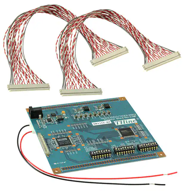
THEVA12LVDR820 Mode Setting & LVDS-Cable
2011/04/14
t=1.6mm
Description
120mm
GND
+12V
RA201
RA202
RA203
RA204
RA205
RA206
FI-X30SSL-HF
THC63LVD824
THC63LVD823B
RES210
RES211
RES212
RES207
RES208
RES209
RES213
R233
RA217
RA218
RA219
RA220
120mm
mm
RA207
RA208
R227
RA209
RA210
RA211
←Low
←High
SW201
SW202
Tx
TEST5
Tx
TEST4
Tx PRBS
Tx /PD
Tx MAP
Tx MAP
Tx MAP
Tx DDRN
Tx RS
Tx RS
Rx
DRVSEL
Rx R/F
Rx TESTO
Rx MODE1
Rx MODE0
FI-X30SSL-HF
SW203
LVDS Cable Type
LVDS-Cable
Type.
JAE
↓
FI-X30HL
・
・
・
・
・
FI-X30HL
JAE
↓
200mm
Copyright© 2011 THine Electronics
Electronics, Inc
Inc.
1/4
THEVA12LVDR820 manual Rev 1 00 E
THEVA12LVDR820_manual_Rev.1.00_E
�THine Electronics, Inc.
THEVA12LVDR820 Mode Setting & LVDS-Cable
2011/04/14
SW201 Setting
SW
Pin#
*
NodeName
Def.
* Def. : Default Setting
THC63LVD824
IC
Pin#
PinName
1
H
RX DRVSEL
9
DRVSEL
2
H
RX R/F
8
R/F
3
L
RX TESTO
7
GND
4
L
RX MODE1
6
MODE1
Description
Output Driverbility Select.
H : High power,
L : Low power.
Output Clock Triggering Edge Select.
H : Rising edge,
L : Falling edge.
Ground Pins for TTL outputs and digital circuitry.
Pixel Data Mode.
MODE1
L
L
MODE0
L
H
Mode
Dual Link
Single Link
5
L
RX MODE0
5
MODE0
6
H
RX /PD
4
/PDWN
H : Normal operation,
L : Power down (all outputs are pulled to ground)
7
L
RX TEST1
3
GND
Ground Pins for TTL outputs and digital circuitry.
8
H
N/C
-
-
Non Connected.
SW202 Setting
SW
Pin#
1
*
Def.
Node
Name
* Def. : Default Setting
THC63LVD823B
IC
Pin#
Description
PinName
LVDS mapping table select.
L
2
H
3
H
4
L
5
L
6
H
7
H
8
H
TX MAP
14
MAP
TX DDRN
13
DDRN
TX RS
12
RS
TX RF
11
R/F
1
L
H(open)
H(open)
SW-Pin#
2
3
H(open) H(open)
L
H(open)
H(open)
L
RS
Mapping Mode
VIHM
VIMM
VILM
Mapping MODE1
Mapping MODE2
Reserved
DDR function is active when
MODE = HL(Single-in/Dual-out mode).
Open or H : DDR(Double Edge input) function disable.
L : DDR(Double Edge input) function enable.
LVDS swing mode, VREF select.
SW-Pin#
RS
5
6
7
L
H(open) H(open)
VIHM
H(open)
L
H(open)
VIMM
H(open) H(open)
L
VILM
a. VREF is Input Reference Voltage.
LVDS Swing
350mV
350mV
200mV
Input Clock Triggering Edge Select.
H : Rising edge,
L : Falling edge
SW203 Setting
SW
Pin#
*
NodeName
Def.
* Def. : Default Setting
THC63LVD823B
1
H
TX TEST5
IC
Pin#
22
2
L
TX TEST4
21
3
L
TX PRBS
20
PRBS
4
H
TX /PD
19
/PDWN
5
L
TX 8/6
18
GND
6
H
TX OE
17
OE
7
L
TX MODE0
16
MODE0
8
L
TX MODE1
Small Swing
Input Support
N/A
RS=VREFa
N/A
15
PinName
N/C
Description
Must be Open.
Reserved Must be tied to GND.
MODE1
Copyright© 2011 THine Electronics
Electronics, Inc
Inc.
PRBS(Pseudo-Random Binary Sequence) generator is active in order to evaluate eye patterns when
MODE = LL(Dual-in/Dual-out mode).
H : PRBS generator is enable.
L : Normal Operation
H : Normal operation,
L : Power down (all outputs are Hi-Z)
Ground Pins for TTL inputs and digital circuitry.
Output enable.
H:O
Output
t t enable,
bl
L : Output disable (all outputs are Hi-Z).
Pixel Data Mode
MODE1
MODE0
L
H
L
H
L
L
H
H
Mode
Dual Link(Dual-in/Dual-out)
Dual Link(Single-in/Dual-out)
Single Link(Dual-in/Single-out)
Single Link(Single-in/Single-out)
2/4
THEVA12LVDR820 manual Rev 1 00 E
THEVA12LVDR820_manual_Rev.1.00_E
�THine Electronics, Inc.
THEVA12LVDR820 Mode Setting & LVDS-Cable
2011/04/14
Measures Type
#
Type
Un-Mount
TTL-I/O
LVDS-input
1
THC63LVD823
B
THC63LVD824
LVDS-output
RES207
RES208
RES209
RES210
RES211
RES212
RES213
R233
TTL-I/O
LVDS-input
THC63LVD823
B
THC63LVD824
0Ω-Mount
LVDS-output
2
RA201
RA202
RA203
RA204
RA205
RA206
RA207
RA208
RA209
RA210
RA211
RA217
RA218
RA219
RA220
R227
RES207
RES208
RES209
RES210
RES211
RES212
RES213
R233
RA201
RA202
RA203
RA204
RA205
RA206
RA207
RA208
RA209
RA210
RA211
RA217
RA218
RA219
RA220
R227
RES207
RES208
RES209
RES210
RES211
RES212
RES213
R233
RA201
RA202
RA203
RA204
RA205
RA206
RA207
RA208
RA209
RA210
RA211
RA217
RA218
RA219
RA220
R227
TTL-moniter
TTL-I/O
LVDS-input
THC63LVD823B
THC63LVD823
B
THC63LVD824
3
TTL-output
TTL-I/O
THC63LVD823
B
THC63LVD824
4
TTL-input
Copyright© 2011 THine Electronics
Electronics, Inc
Inc.
3/4
LVDS-output
RA201
RA202
RA203
RA204
RA205
RA206
RA207
RA208
RA209
RA210
RA211
RA217
RA218
RA219
RA220
R227
33Ω-Mount
RES207
RES208
RES209
RES210
RES211
RES212
RES213
R233
THEVA12LVDR820 manual Rev 1 00 E
THEVA12LVDR820_manual_Rev.1.00_E
�THine Electronics, Inc.
THEVA12LVDR820 Mode Setting & LVDS-Cable
2011/04/14
Notices and Requests
1. The product specifications described in this material are subject to change without prior notice.
2. The circuit diagrams
described in this material are examples
which may
g
p of the application
pp
y not always
y
apply to the customer’s design. We are not responsible for possible errors and omissions in this material.
Please note if errors or omissions should be found in this material, we may not be able to correct them
3. This material contains our copy right, know-how or other proprietary. Copying or disclosing to third parties
the contents of this material without our prior permission is prohibited.
4. Note that if infringement of any third party's industrial ownership should occur by using this product, we will be
e e pted from
o tthee responsibility
espo s b ty uunless
ess itt ddirectly
ect y relates
e ates to tthee production
p oduct o pprocess
ocess oor functions
u ct o s oof tthee pproduct.
oduct.
exempted
5. This product is presumed to be used for general electric equipment, not for the applications which require very hi
reliability (including medical equipment directly concerning people's life, aerospace equipment, or nuclear contro
equipment). Also, when using this product for the equipment concerned with the control and safety of the
transportation means, the traffic signal equipment, or various Types of safety equipment, please do it after applyin
appropriate measures to the product.
6. Despite our utmost efforts to improve the quality and reliability of the product, faults will occur with a certain
small probability, which is inevitable to a semi-conductor product. Therefore, you are encouraged to have suffici
redundant or error preventive design applied to the use of the product so as not to have our product cause any soc
or public damage.
7. Please note that this product is not designed to be radiation-proof.
8. Customers are asked, if required, to judge by themselves if this product falls under the category of strategic good
under the Foreign Exchange and Foreign Trade Control Law.
Law
THine Electronics, Inc.
sales@thine.co.jp
Copyright© 2011 THine Electronics, Inc.
4/4
THEVA12LVDR820_manual_Rev.1.00_E
�
很抱歉,暂时无法提供与“THEVA12LVDR820”相匹配的价格&库存,您可以联系我们找货
免费人工找货