NPN SILICON HIGH FREQUENCY TRANSISTOR
FEATURES
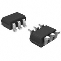
• • • • SMALL PACKAGE STYLE: 2 NE856 Die in a 2 mm x 1.25 mm package LOW NOISE FIGURE: NF = 1.2 dB TYP at 1 GHz HIGH GAIN: |S21E|2 = 9.0 dB TYP at 1 GHz HIGH COLLECTOR CURRENT: 100mA
0.65 2.0 ± 0.2 1
UPA801T
OUTLINE DIMENSIONS (Units in mm)
PACKAGE OUTLINE S06 (Top View) 2.1 ± 0.1
1.25 ± 0.1
6 0.2 (All Leads)
DESCRIPTION
NEC's UPA801T is two NPN high frequency silicon epitaxial transistors encapsulated in an ultra small 6 pin SMT package. Each transistor is independently mounted and easily configured for either dual transistor or cascode operation. The high fT, low voltage bias and small size make this device ideally suited for pager and other hand-held wireless applications.
1.3
2
5
3
4
0.9 ± 0.1 0.7 0.15 - 0.05
PIN OUT 0 ~ 0.1 1. Collector Transistor 1 2. Emitter Transistor 1 3. Collector Transistor 2 4. Emitter Transistor 2 5. Base Transistor 2 6. Base Transistor 1 Note: Pin 3 is identified with a circle on the bottom of the package.
+0.10
ELECTRICAL CHARACTERISTICS (TA = 25°C)
PART NUMBER PACKAGE OUTLINE SYMBOLS ICBO IEBO hFE1 fT Cre2 |S21E|2 NF hFE1/hFE2 PARAMETERS AND CONDITIONS Collector Cutoff Current at VCB = 10 V, IE = 0 Emitter Cutoff Current at VEB = 1 V, IC = 0 Forward Current Gain at VCE = 3 V, IC = 7 mA Gain Bandwidth at VCE = 3 V, IC = 7 mA Feedback Capacitance at VCB = 3 V, IE = 0, f = 1 MHz Insertion Power Gain at VCE = 3 V, IC = 7 mA, f = 1 GHz Noise Figure at VCE = 3 V, IC = 7 mA, f = 1 GHz hFE Ratio: hFE1 = Smaller Value of Q1 or Q2 hFE2 = Larger Value pf Q1 or Q2 GHz pF dB dB 0.85 7 UNITS µA µA 70 3.0 120 4.5 0.7 9 1.2 2.5 1.5 MIN UPA801T S06 TYP MAX 1.0 1.0 250
Notes: 1.Pulsed measurement, pulse width ≤ 350 µs, duty cycle ≤ 2 %. 2.The emitter terminal should be connected to the ground terminal of the 3 terminal capacitance bridge. For Tape and Reel version use part number UPA801T-T1, 3K per reel. .
California Eastern Laboratories
�UPA801T ABSOLUTE MAXIMUM RATINGS1 (TA = 25°C)
SYMBOLS VCBO VCEO VEBO IC PT PARAMETERS Collector to Base Voltage Collector to Emitter Voltage Emitter to Base Voltage Collector Current Total Power Dissipation 1 Die 2 Die Junction Temperature Storage Temperature UNITS V V V mA mW mW °C °C RATINGS 20 12 3 100 110 200 150 -65 to +150
TJ TSTG
Note: 1. Operation in excess of any one of these parameters may result in permanent damage.
TYPICAL PERFORMANCE CURVES (TA = 25°C)
TOTAL POWER DISSIPATION vs. AMBIENT TEMPERATURE
20
COLLECTOR CURRENT vs. BASE TO EMITTER VOLTAGE
VCE = 3 V
Total Power Dissipation, PT (mW)
em
en
ts
Pe
in
rE
lem
To t
al
en
Collector Current, IC (mA)
200
2
El
t
10
100
0
50
100
150
0
0.5
1.0
Ambient Temperature, TA (°C)
Base to Emitter Voltage, VBE (V)
COLLECTOR CURRENT vs. COLLECTOR TO EMITTER VOLTAGE
25 lB=160 µA 140 µA 200
DC CURRENT GAIN vs. COLLECTOR CURRENT
VCE = 3 V
Collector Current, IC (mA)
120 µA 15 100 µA 80 µA 10 60 µA 40 µA 5 20 µA
DC Current Gain, hFE
10
20
100
50
20
10 0 5 0.5 1 5 10 50
Collector to Emitter Voltage, VCE (V)
Collector Current, IC (mA)
�UPA801T TYPICAL PERFORMANCE CURVES (TA = 25°C)
GAIN BANDWIDTH PRODUCT vs. COLLECTOR CURRENT
20
15
INSERTION POWER GAIN vs. COLLECTOR CURRENT
Gain Bandwidth Product, fT (GHz)
10
Insertion Power Gain, IS21eI2 (dB)
VCE = 3 V f = 1 GHz
VCE = 3 V f = 1 GHz
10
5
5
2
1 0.5 1 5 10 50
0 0.5 1 5 10 50 100
Collector Current, IC (mA)
Collector Current, IC (mA)
NOISE FIGURE vs. COLLECTOR CURRENT
6 24 VCE = 3 V f = 1 GHz
INSERTION POWER GAIN vs. FREQUENCY
VCE = 3 V lc = 7 mA 20
Insertion Power Gain, IS21eI2 (dB)
Noise Figure (dB)
4
16
12
2
8
4
0 0.5 1.0 5.0 10 50 100
0 0.1 0.2 0.5 1.0 2.0 5.0
Collector Current, IC (mA)
Frequency, f (GHz)
FEED BACK CAPACITANCE vs. COLLECTOR TO BASE VOLTAGE
5.0 f = 1 MHz
Feed Back Capacitance, CRE (pF)
2.0
1.0
0.5
0.2
0.1 1 2 5 10 20 50
Collector to Base Voltage, VCB (V)
�UPA801T TYPICAL SCATTERING PARAMETERS (TA = 25°C)
UPA801T VCE = 3 V, IC = 1 mA, Z0 = 50 Ω
FREQUENCY (GHz) 0.10 0.20 0.30 0.40 0.50 0.60 0.70 0.80 0.90 1.00 1.10 1.20 1.30 1.40 1.50 1.60 1.70 1.80 1.90 2.00 MAG .967 .930 .884 .842 .801 .771 .742 .722 .706 .696 .689 .685 .681 .681 .683 .684 .684 .686 .689 .690 S11 ANG -22.9 -45.8 -67.1 -86.9 -103.1 -117.0 -130.0 -141.2 -151.1 -159.9 -167.7 -174.9 178.7 172.6 166.8 161.4 156.1 151.4 146.6 142.1 MAG 1.935 1.968 1.938 1.827 1.748 1.576 1.498 1.403 1.326 1.242 1.169 1.102 1.030 .979 .925 .884 .842 .804 .773 .738 S21 ANG 159.9 143.1 129.1 117.2 106.7 97.4 89.2 81.9 75.6 69.6 64.5 59.6 55.3 50.9 47.2 43.6 40.4 37.3 34.6 32.3 MAG .045 .083 .108 .125 .134 .137 .137 .134 .129 .124 .118 .112 .106 .103 .100 .102 .107 .115 .127 .141 S12 ANG 74.0 60.1 48.9 39.4 32.6 27.1 22.9 20.0 18.5 17.8 18.1 19.8 23.5 28.0 33.6 40.4 47.5 53.5 57.9 62.1 MAG .978 .931 .870 .822 .779 .749 .722 .702 .690 .680 .671 .666 .660 .658 .654 .651 .651 .649 .646 .646 S22 ANG -9.2 -17.4 -23.2 -28.0 -31.9 -35.3 -38.4 -41.3 -44.4 -47.4 -50.4 -53.6 -56.9 -60.4 -64.0 -67.6 -71.5 -75.1 -79.2 -83.0
VCE = 3 V, IC = 3 mA, Z0 = 50 Ω
FREQUENCY (GHz) 0.10 0.20 0.30 0.40 0.50 0.60 0.70 0.80 0.90 1.00 1.10 1.20 1.30 1.40 1.50 1.60 1.70 1.80 1.90 2.00 MAG .899 .808 .723 .660 .610 .583 .560 .547 .538 .535 .534 .533 .533 .534 .538 .542 .545 .548 .552 .556 S11 ANG -30.5 -60.0 -86.7 -106.2 -125.9 -138.6 -150.0 -159.4 -167.4 -174.4 179.3 173.4 168.3 163.2 158.7 154.3 150.0 146.1 142.0 138.3 MAG 5.578 5.327 4.877 4.341 3.883 3.388 3.046 2.741 2.498 2.287 2.111 1.965 1.830 1.721 1.620 1.544 1.464 1.396 1.336 1,280 S21 ANG 153.7 134.4 119.6 108.1 98.5 90.9 84.3 78.5 73.4 68.9 64.6 60.2 56.3 52.7 49.2 45.7 42.7 39.5 36.6 33.6 MAG .042 .069 .084 .093 .098 .102 .106 .108 .112 .116 .120 .125 .131 .139 .146 .155 .164 .174 .187 .199 S12 ANG 69.0 54.5 46.0 41.1 38.8 37.4 37.8 38.1 39.5 41.0 43.0 45.1 46.7 48.3 49.8 51.3 52.4 53.0 53.7 54.1 MAG .923 .793 .679 .604 .550 .613 .487 .468 .455 .444 .435 .429 .424 .422 .417 .414 .415 .412 .411 .411 S22 ANG -17.3 -29.2 -36.4 -39.5 -42.0 -44.2 -45.9 -47.9 -49.9 -52.3 -54.7 57.2 -59.9 -62.8 -65.7 -68.8 -72.0 -75.3 -78.8 -82.3
�UPA801T TYPICAL SCATTERING PARAMETERS (TA = 25°C)
VCE = 3 V, IC = 5 mA, Z0 = 50 Ω
FREQUENCY (GHz) 0.10 0.20 0.30 0.40 0.50 0.60 0.70 0.80 0.90 1.00 1.10 1.20 1.30 1.40 1.50 1.60 1.70 1.80 1.90 2.00 MAG .819 .701 .608 .549 .511 .494 .481 .475 .472 .471 .473 .474 .474 .477 .481 .484 .489 .490 .495 .501 S11 ANG -38.9 -73.4 -102.3 -123.6 -139.6 -151.0 -160.8 -168.6 -175.7 178.2 172.8 167.6 162.9 158.4 154.4 150.3 146.5 142.9 139.3 136.0 MAG 8.934 8.007 6.898 5.819 4.970 4.255 3.750 3.328 3.004 2.734 2.522 2.355 2.176 2..038 1.921 1.818 1.726 1.647 1.578 1.505 S21 ANG 148.0 127.6 112.6 101.8 93.5 86.9 81.4 76.3 72.0 67.7 64.0 60.2 56.7 53.2 49.8 46.7 43.9 40.6 37.6 35.0 MAG .038 .060 .072 .079 .086 .093 .099 .107 .113 .122 .130 .139 .148 .158 .168 .177 .190 .200 .212 .223 S12 ANG 65.8 53.1 47.6 45.2 45.7 46.5 47.2 48.9 49.7 50.9 51.6 52.3 53.1 53.3 53.7 53.3 53.3 53.0 52.7 52.0 MAG .868 .687 .560 .483 .434 .402 .379 .361 .350 .340 .332 .328 .322 .319 .315 .313 .312 .312 .309 .309 S22 ANG -23.6 -36.7 -42.4 -45.4 -47.2 -48.6 -49.9 -51.5 -53.4 -55.4 -57.3 59.7 -62.3 -65.2 -68.2 -70.9 -73.9 -77.2 -80.8 -84.0
VCE = 3 V, IC = 7 mA, Z0 = 50 Ω
FREQUENCY (GHz) 0.10 0.20 0.30 0.40 0.50 0.60 0.70 0.80 0.90 1.00 1.10 1.20 1.30 1.40 1.50 1.60 1.70 1.80 1.90 2.00 MAG .750 .618 .528 .483 .459 .447 .441 .439 .437 .437 .440 .443 .444 .449 .450 .455 .459 .462 .466 .470 S11 ANG -45.7 -84.9 -114.5 -134.3 -148.5 -158.8 -167.4 -174.4 179.2 173.7 168.6 163.9 159.6 155.5 151.6 147.9 144.3 140.9 137.5 134.4 MAG 11.858 10.093 8.219 6.684 5.565 4.737 4.134 3.653 3.283 2.978 2.732 2.533 2.357 2.216 2.077 1.972 1.868 1.789 1.702 1.635 S21 ANG 144.0 122.3 107.7 97.9 90.5 84.6 79.7 75.2 71.1 67.2 63.7 60.0 66.6 53.4 50.3 47.4 44.3 41.3 38.4 36.1 MAG .035 .053 .054 .073 .081 .089 .098 .107 .117 .126 .136 .147 .158 .169 .180 .192 .202 .214 .226 .238 S12 ANG 63.3 53.2 50.6 50.6 50.7 52.3 53.5 54.2 54.9 55.6 55.8 55.3 55.4 55.3 54.7 64.5 53.9 53.0 52.3 51.5 MAG .816 .609 .481 .411 .365 .337 .337 .300 .290 .281 .275 .270 .267 .264 .259 .258 .256 .255 .253 .253 S22 ANG -28.5 -41.8 -46.7 -49.1 -50.5 -51.5 -51.5 -54.2 -55.9 -57.9 -59.8 -52.3 -64.7 -67.5 -70.5 -73.3 -76.3 -79.6 -83.0 -86.4
ORDERING INFORMATION
PART NUMBER UPA801T-T1-A QUANTITY 3000 PACKAGING Tape & Reel
�UPA801T NONLINEAR MODEL
BJT NONLINEAR MODEL PARAMETERS (1)
Parameters IS BF NF VAF IKF ISE NE BR NR VAR IKR ISC NC RE RB RBM IRB RC CJE VJE MJE CJC VJC Q1, Q2 6e-16 120 0.98 10 0.08 32e-16 1.93 12 0.991 3.9 0.17 0 2 0.38 4.16 3.6 1.96e-4 2 2.8e-12 1.3 0.5 1.1e-12 0.7 Parameters MJC XCJC CJS VJS MJS FC TF XTF VTF ITF PTF TR EG XTB XTI KF AF Q1, Q2 0.55 0.3 0 0.75 0 0.5 12e-12 6 10 0.2 0 1e-9 1.11 0 3 1.56e-18 1.49
UNITS
Parameter time capacitance inductance resistance voltage current Units seconds farads henries ohms volts amps
MODEL RANGE Frequency: 0.1 to 3.0 GHz Bias: VCE = 1 V to 5 V, IC = 1 mA to 10 mA Date: 12/98
(1) Gummel-Poon Model Note: This nonlinear model utilized the latest data available. See our Design Parameter Library at www.cel.com for this data.
�UPA801T NONLINEAR MODEL SCHEMATIC
0.07 pF C_C1B2 0.1 pF CCBPKG1 LC Pin_1 0.05 nH 0.07 pF CCB1 LB1 C_C1E1 0.05 pF LE Pin_2 0.05 nH CCE1 0.1 pF LE1 0.82 nH C_E1B2 0.1 pF LB2 0.6 nH C_B1B2 0.05 pF LB 0.05 nH C_B2E2 0.05 pF LE2 0.65 nH 0.1 pF CCE2 0.1 pF CCEPKG2 0.06 pF CCBPKG2 LE 0.05 nH Pin_4 Pin_5 LB 0.05 nH Pin_6
Q1
0.6 nH
C_E1C2 0.05 pF CCB2 0.07 pF
Q2
LC Pin_3 0.05 nH
MODEL RANGE Frequency: 0.1 to 3.0 GHz Bias: VCE = 1 V to 5 V, IC = 1 mA to 10 mA Date: 12/98
Life Support Applications These NEC products are not intended for use in life support devices, appliances, or systems where the malfunction of these products can reasonably be expected to result in personal injury. The customers of CEL using or selling these products for use in such applications do so at their own risk and agree to fully indemnify CEL for all damages resulting from such improper use or sale.
EXCLUSIVE NORTH AMERICAN AGENT FOR RF, MICROWAVE & OPTOELECTRONIC SEMICONDUCTORS
CALIFORNIA EASTERN LABORATORIES • Headquarters • 4590 Patrick Henry Drive • Santa Clara, CA 95054-1817 • (408) 988-3500 • Telex 34-6393 • FAX (408) 988-0279 24-Hour Fax-On-Demand: 800-390-3232 (U.S. and Canada only) • Internet: http://WWW.CEL.COM 9/99 DATA SUBJECT TO CHANGE WITHOUT NOTICE
�4590 Patrick Henry Drive Santa Clara, CA 95054-1817 Telephone: (408) 919-2500 Facsimile: (408) 988-0279
Subject: Compliance with EU Directives
CEL certifies, to its knowledge, that semiconductor and laser products detailed below are compliant with the requirements of European Union (EU) Directive 2002/95/EC Restriction on Use of Hazardous Substances in electrical and electronic equipment (RoHS) and the requirements of EU Directive 2003/11/EC Restriction on Penta and Octa BDE. CEL Pb-free products have the same base part number with a suffix added. The suffix –A indicates that the device is Pb-free. The –AZ suffix is used to designate devices containing Pb which are exempted from the requirement of RoHS directive (*). In all cases the devices have Pb-free terminals. All devices with these suffixes meet the requirements of the RoHS directive. This status is based on CEL’s understanding of the EU Directives and knowledge of the materials that go into its products as of the date of disclosure of this information.
Restricted Substance per RoHS Lead (Pb) Mercury Cadmium Hexavalent Chromium PBB PBDE Concentration Limit per RoHS (values are not yet fixed) < 1000 PPM < 1000 PPM < 100 PPM < 1000 PPM < 1000 PPM < 1000 PPM Concentration contained in CEL devices -A Not Detected Not Detected Not Detected Not Detected Not Detected Not Detected -AZ (*)
If you should have any additional questions regarding our devices and compliance to environmental standards, please do not hesitate to contact your local representative.
Important Information and Disclaimer: Information provided by CEL on its website or in other communications concerting the substance content of its products represents knowledge and belief as of the date that it is provided. CEL bases its knowledge and belief on information provided by third parties and makes no representation or warranty as to the accuracy of such information. Efforts are underway to better integrate information from third parties. CEL has taken and continues to take reasonable steps to provide representative and accurate information but may not have conducted destructive testing or chemical analysis on incoming materials and chemicals. CEL and CEL suppliers consider certain information to be proprietary, and thus CAS numbers and other limited information may not be available for release. In no event shall CEL’s liability arising out of such information exceed the total purchase price of the CEL part(s) at issue sold by CEL to customer on an annual basis. See CEL Terms and Conditions for additional clarification of warranties and liability.
�