PRELIMINARY DATA SHEET
SILICON TRANSISTOR
UPA810T
NPN SILICON HIGH
FREQUENCY TRANSISTOR
OUTLINE DIMENSIONS (Units in mm)
FEATURES
•
•
•
•
•
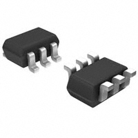
PACKAGE OUTLINE S06
(Top View)
SMALL PACKAGE STYLE:
2 NE856 Die in a 2 mm x 1.25 mm package
2.1 ± 0.1
LOW NOISE FIGURE:
NF = 1.2 dB TYP at 1 GHz
1.25 ± 0.1
HIGH GAIN:
|S21E|2 = 9.0 dB TYP at 1 GHz
EXCELLENT LOW VOLTAGE, LOW CURRENT
PERFORMANCE
HIGH COLLECTOR CURRENT: 100 mA
0.65
2.0 ± 0.2
1.3
DESCRIPTION
The UPA810T is two NPN high frequency silicon epitaxial
transistors encapsulated in an ultra small 6 pin SMT package.
Each transistor is independently mounted and easily configured for either dual transistor or cascode operation. The high
fT, low voltage bias and small size make this device suited for
various hand-held wireless applications.
1
6
2
5
3
4
0.2 (All Leads)
0.9 ± 0.1
0.7
0.15 - 0.05
PIN OUT
1. Collector Transistor 1
2. Base Transistor 2
3. Collector Transistor 2
4. Emitter Transistor 2
5. Emitter Transistor 1
6. Base Transistor 1
0 ~ 0.1
Note:
Pin 3 is identified with a circle on the bottom of the package.
ELECTRICAL CHARACTERISTICS (TA = 25°C)
PART NUMBER
PACKAGE OUTLINE
SYMBOLS
PARAMETERS AND CONDITIONS
UPA810T
S06
UNITS
MIN
TYP
MAX
ICBO
Collector Cutoff Current at VCB = 10 V, IE = 0
μA
1.0
IEBO
Emitter Cutoff Current at VEB = 1 V, IC = 0
μA
1.0
hFE1
fT
Cre2
|S21E|2
NF
hFE1/hFE2
Forward Current Gain at VCE = 3 V, IC = 7 mA
Gain Bandwidth at VCE = 3 V, IC = 7 mA
GHz
Feedback Capacitance at VCB = 3 V, IE = 0, f = 1 MHz
pF
Insertion Power Gain at VCE = 3 V, IC =7 mA, f = 1 GHz
dB
Noise Figure at VCE = 3 V, IC = 7 mA, f = 1 GHz
dB
hFE Ratio: hFE1 = Smaller Value of Q1, or Q2
hFE2 = Larger Value of Q1 or Q2
70
120
3.0
4.5
0.7
7
1.5
9
1.2
0.85
Notes: 1. Pulsed measurement, pulse width ≤ 350 μs, duty cycle ≤ 2 %.
2. The emitter terminal should be connected to the ground terminal of the 3 terminal capacitance bridge.
For Tape and Reel version use part number UPA810T-T1, 3K per reel.
The information in this document is subject to change without notice. Before using this document, please confirm
that this is the latest version.
Date Published: June 28, 2005
250
2.5
�UPA810T
ABSOLUTE MAXIMUM RATINGS1 (TA = 25°C)
SYMBOLS
PARAMETERS
UNITS
RATINGS
VCBO
Collector to Base Voltage
V
20
VCEO
Collector to Emitter Voltage
V
12
VEBO
Emitter to Base Voltage
V
3
IC
Collector Current
mA
100
PT
Total Power Dissipation
1 Die
2 Die
mW
mW
110
200
TJ
Junction Temperature
°C
150
TSTG
Storage Temperature
°C
-65 to +150
Note: 1.Operation in excess of any one of these parameters
may result in permanent damage.
ORDERING INFORMATION (Solder Contains Lead)
PART NUMBER
QUANTITY
UPA810T
Loose Products (50 pcs)
UPA810T-T1
Taping products
PACKAGING
Embossed tape 8mm wide. Pin 6 (Q1 Base),
Pin 5 (Q1 Emmitter) Pin 4 (Q2 Emitter)
face to perforation side of tape
(3 KPCS/Reel)
ORDERING INFORMATION (Pb-Free)
PART NUMBER
QUANTITY
UPA810T-A
Loose Products (50 pcs)
UPA810T-T1-A
Taping products
(3 KPCS/Reel)
PACKAGING
Embossed tape 8mm wide. Pin 6 (Q1 Base),
Pin 5 (Q1 Emmitter) Pin 4 (Q2 Emitter)
face to perforation side of tape
�
很抱歉,暂时无法提供与“UPA810T-T1-A”相匹配的价格&库存,您可以联系我们找货
免费人工找货