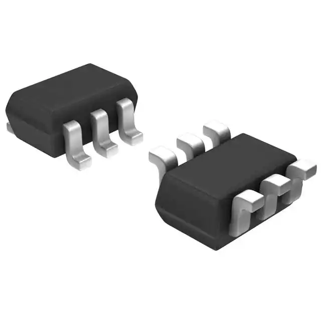
3 V SILICON RFIC FREQUENCY UPCONVERTER
FEATURES
• RECOMMENDED OPERATING FREQUENCY: fRFOUT = 0.8 GHz to 2.0 GHz fIFIN = 50 MHz to 300 MHz • SUPPLY VOLTAGE: VCC = 2.7 to 3.3 V • HIGH DENSITY SURFACE MOUNTING: 6-pin super minimold package • HIGH IP3: OIP3 = +9.5 dBm @ fRFOUT = 900 MHz • MINIMIZED CARRIER LEAKAGE: Due to double balanced mixer
IF input 1 LO input 3
UPC8163TB
BLOCK DIAGRAM
(Top View)
4
GND
GND
2
5
VCC
6 RF output
DESCRIPTION
NEC's UPC8163TB is a silicon RFIC designed as a frequency upconverter for cellular/cordless telephone transmitter stages, and features improved intermodulation. This device is housed in a 6 pin super mini mold or SOT-363 package making it ideal for reducing system size. The UPC8106TB is manufactured using NEC's 20 GHz fT NESATTM III silicon bipolar process. NEC's stringent quality assurance and test procedures ensure the highest reliability and performance.
APPLICATIONS
• Digital Cellular/Cordless Phones
ELECTRICAL CHARACTERISTICS
(TA = 25°C, VCC = VRFOUT = 3.0 V, fIFIN = 240 MHz, PLOIN = -5 dBm unless otherwise specified) PART NUMBER PACKAGE OUTLINE SYMBOLS ICC CG PSAT OIP3 PARAMETERS AND CONDITIONS Circuit Current (no signal) Conversion Gain Saturated Output Power fRFOUT = 0.9 GHz, PIFIN = -30 dBm fRFOUT = 1.9 GHz, PIFIN = -30 dBm fRFOUT = 0.9 GHz fRFOUT = 1.9 GHz UNITS mA dB dB dBm dBm MIN 11.5 6 4 -1.5 -4.5 UPC8163TB S06 TYP 16.5 9 7 0.5 -2 MAX 23 12 10
Output third Order Intercept Point, fIFIN1 = 240 MHz fIFIN2 = 240.4 MHz PIFIN = -20 dBm SSB Noise Figure
fRFOUT = 0.9 GHz fRFOUT = 1.9 GHz
dBm dBm dB dB
+9.5 +6.0 12.5 12.5
NF
fRFOUT = 0.9 GHz fRFOUT = 1.9 GHz
California Eastern Laboratories
�UPC8163TB ABSOLUTE MAXIMUM RATINGS1 (TA = 25°C)
SYMBOLS VCC PT PIN TOP TSTG PARAMETERS Supply Voltage2 Total Power Input Power Operating Temperature Storage Temperature Dissipation3 UNITS V mW dBm °C °C RATINGS 3.6 200 +10 -40 to +85 -55 to +150
RECOMMENDED OPERATING CONDITIONS
SYMBOLS VCC PLOIN fRFOUT fIFIN TOP PARAMETERS Supply Voltage1 Local Input Level2 RF Output Frequency3 IF Input Frequency Operating Temperature UNITS MIN V dBm GHz MHz ˚C 2.7 -10 0.8 50 -40 TYP MAX 3.0 -5 – – +25 3.3 0 2.0 300 +85
Notes: 1. Operation in excess of any one of these conditions may result in permanent damage. 2. TA = 25˚C, pins 5 and 6. 3. Mounted on a double-sided copperclad 50x50x1.6 mm epoxy glass PWB, TA = 85˚C).
Notes: 1. Same voltage applied to pins 5 and 6 2. ZS = 50 Ω (without matching) 3. With external matching circuit
PIN FUNCTIONS
Pin No. 1 Pin Name IFINPUT Applied Voltage — Pin Voltage 1.2 Description This pin is the IF input to double balanced mixer. The input is a high impedance. GND pin. Ground pattern on the board should be as wide as possible. Trace length should be kept as short as possible to minimize ground impedance. LO input pin. Recommended input level is -10 to 0 dBm. Supply voltage pin. This pin is the RF output. This pin is designed as an open collector. Due to the high impedance output, this pin requires an external LC matching circuit. Equivalent Circuit
2 4
GND
0
—
5 6 3
3
LOINPUT
—
2.1
1
5 6
VCC
2.7 to 3.3
— —
RFOUTPUT Same bias as VCC through external inductor
2
APPLICATION EXAMPLE
RX DEMO I Q
VCO SW
÷N
PLL PLL
I 0˚ TX PA UPC8163TB Phase Shifter 90˚ Q
�UPC8163TB OUTLINE DIMENSIONS (Units in mm)
PACKAGE OUTLINE S06
2.1±0.1 1.25±0.1 2.0±0.2 0.65 3 1.3 0.65 2
LEAD CONNECTIONS
(Top View) (Bottom View)
3
4 0.2 +0.1 -0
C2Y
4 5 6
4 5 6
3 2 1
2 1
5
1
6
DOT ON BACK SIDE
0.9 ± 0.1 0.7
0 ~0.1
+0.1 0.15 -0.5
1. 2. 3. 4. 5. 6.
IF INPUT GND LO INPUT GND VCC RF OUTPUT
Note: All dimensions are typical unless otherwise specified.
ORDERING INFORMATION
PART NUMBER UPC8163TB-E3-A QUANTITY 3K/Reel
Note: Embossed tape 8 mm wide. Pins 1,2,3 face tape perforation side.
TEST CIRCUIT 1 (RFOUT = 900 MHz)
(Top View)
100 pF
TEST CIRCUIT 2 (RFOUT = 1.9 GHz)
(Top View)
100 pF
3 LOin
GND
4
3 LOin
GND
4
2 GND
100 pF
VCC
5
2 GND
10 nH 1.0 pF 1000 pF 1000 pF 0.1 µF
100 pF
VCC
5
100 nH TL = 5 nH
1000 pF 1000 pF
0.1 µF
1 IFin
RFout 6
900 MHz Match
1 IFin
RFout 6
2.7 pF 1.9 GHz Match
Life Support Applications These NEC products are not intended for use in life support devices, appliances, or systems where the malfunction of these products can reasonably be expected to result in personal injury. The customers of CEL using or selling these products for use in such applications do so at their own risk and agree to fully indemnify CEL for all damages resulting from such improper use or sale.
EXCLUSIVE NORTH AMERICAN AGENT FOR
RF, MICROWAVE & OPTOELECTRONIC SEMICONDUCTORS
CALIFORNIA EASTERN LABORATORIES • Headquarters • 4590 Patrick Henry Drive • Santa Clara, CA 95054-1817 • (408) 988-3500 • Telex 34-6393 • FAX (408) 988-0279 24-Hour Fax-On-Demand: 800-390-3232 (U.S. and Canada only) • Internet: http://WWW.CEL.COM 02/14/2000 DATA SUBJECT TO CHANGE WITHOUT NOTICE
5-142
�4590 Patrick Henry Drive Santa Clara, CA 95054-1817 Telephone: (408) 919-2500 Facsimile: (408) 988-0279
Subject: Compliance with EU Directives
CEL certifies, to its knowledge, that semiconductor and laser products detailed below are compliant with the requirements of European Union (EU) Directive 2002/95/EC Restriction on Use of Hazardous Substances in electrical and electronic equipment (RoHS) and the requirements of EU Directive 2003/11/EC Restriction on Penta and Octa BDE. CEL Pb-free products have the same base part number with a suffix added. The suffix –A indicates that the device is Pb-free. The –AZ suffix is used to designate devices containing Pb which are exempted from the requirement of RoHS directive (*). In all cases the devices have Pb-free terminals. All devices with these suffixes meet the requirements of the RoHS directive. This status is based on CEL’s understanding of the EU Directives and knowledge of the materials that go into its products as of the date of disclosure of this information.
Restricted Substance per RoHS Lead (Pb) Mercury Cadmium Hexavalent Chromium PBB PBDE Concentration Limit per RoHS (values are not yet fixed) < 1000 PPM < 1000 PPM < 100 PPM < 1000 PPM < 1000 PPM < 1000 PPM Concentration contained in CEL devices -A Not Detected Not Detected Not Detected Not Detected Not Detected Not Detected -AZ (*)
If you should have any additional questions regarding our devices and compliance to environmental standards, please do not hesitate to contact your local representative.
Important Information and Disclaimer: Information provided by CEL on its website or in other communications concerting the substance content of its products represents knowledge and belief as of the date that it is provided. CEL bases its knowledge and belief on information provided by third parties and makes no representation or warranty as to the accuracy of such information. Efforts are underway to better integrate information from third parties. CEL has taken and continues to take reasonable steps to provide representative and accurate information but may not have conducted destructive testing or chemical analysis on incoming materials and chemicals. CEL and CEL suppliers consider certain information to be proprietary, and thus CAS numbers and other limited information may not be available for release. In no event shall CEL’s liability arising out of such information exceed the total purchase price of the CEL part(s) at issue sold by CEL to customer on an annual basis. See CEL Terms and Conditions for additional clarification of warranties and liability.
5-143
�5-144
�
很抱歉,暂时无法提供与“UPC8163TB-E3-A”相匹配的价格&库存,您可以联系我们找货
免费人工找货