CP710V-MPSA92
PNP - High Voltage Transistor Die
w w w. c e n t r a l s e m i . c o m
The CP710V-MPSA92 is a silicon PNP transistor designed for high voltage applications.
MECHANICAL SPECIFICATIONS:
Die Size
B
E
BACKSIDE COLLECTOR
R2
26 x 26 MILS
Die Thickness
7.1 MILS
Base Bonding Pad Size
6.1 x 4.9 MILS
Emitter Bonding Pad Size
5.2 x 5.2 MILS
Top Side Metalization
Al – 30,000Å
Back Side Metalization
Au – 9,000Å
Scribe Alley Width
2.2 MILS
Wafer Diameter
5 INCHES
Gross Die Per Wafer
25,214
MAXIMUM RATINGS: (TA=25°C)
Collector-Base Voltage
Collector-Emitter Voltage
Emitter-Base Voltage
Continuous Collector Current
Operating and Storage Junction Temperature
SYMBOL
VCBO
VCEO
300
UNITS
V
300
V
5.0
V
500
mA
-65 to +150
°C
VEBO
IC
TJ, Tstg
MIN
MAX
250
UNITS
nA
100
nA
ELECTRICAL
SYMBOL
ICBO
IEBO
CHARACTERISTICS: (TA=25°C)
TEST CONDITIONS
VCB=200V
VEB=3.0V
BVCBO
IC=100µA
300
V
BVCEO
IC=1.0mA
300
V
BVEBO
IE=100µA
5.0
VCE(SAT)
VBE(SAT)
IC=20mA, IB=2.0mA
IC=20mA, IB=2.0mA
hFE
hFE
VCE=10V, IC=1.0mA
VCE=10V, IC=10mA
25
hFE
25
fT
VCE=10V, IC=30mA
VCE=20V, IC=10mA, f=100MHz
Cob
VCB=20V, IE=0, f=1.0MHz
V
0.5
V
0.9
V
40
50
MHz
6.0
pF
R1 (1-August 2016)
�CP710V-MPSA92
Typical Electrical Characteristics
w w w. c e n t r a l s e m i . c o m
R1 (1-August 2016)
�BARE DIE PACKING OPTIONS
BARE DIE IN TRAY (WAFFLE) PACK
CT: �Singulated die in tray (waffle) pack.
(example: CP211-PART NUMBER-CT)
CM: S
� ingulated die in tray (waffle) pack 100% visually inspected as
per MIL-STD-750, (method 2072 transistors, method 2073 diodes).
(example: CP211-PART NUMBER-CM)
UNSAWN WAFER
WN: �Full wafer, unsawn, 100% tested with reject die inked.
(example: CP211-PART NUMBER-WN)
SAWN WAFER ON PLASTIC RING
WR: F
� ull wafer, sawn and mounted on plastic ring,
100% tested with reject die inked.
(example: CP211-PART NUMBER-WR)
Please note: Sawn Wafer on Metal Frame (WS)
is possible as a special order. Please contact your
Central Sales Representative at 631-435-1110.
Visit the Central website for a complete listing of specifications:
www.centralsemi.com/bdspecs
R2 (3-April 2017)
w w w. c e n t r a l s e m i . c o m
�OUTSTANDING SUPPORT AND SUPERIOR SERVICES
PRODUCT SUPPORT
Central’s operations team provides the highest level of support to insure product is delivered on-time.
• Supply management (Customer portals)
• Custom bar coding for shipments
• Inventory bonding
• Custom product packing
• Consolidated shipping options
DESIGNER SUPPORT/SERVICES
Central’s applications engineering team is ready to discuss your design challenges. Just ask.
• Free quick ship samples (2nd day air)
• Special wafer diffusions
• Online technical data and parametric search
• PbSn plating options
• SPICE models
• Package details
• Custom electrical curves
• Application notes
• Environmental regulation compliance
• Application and design sample kits
• Customer specific screening
• Custom product and package development
• Up-screening capabilities
REQUESTING PRODUCT PLATING
1. If requesting Tin/Lead plated devices, add the suffix “ TIN/LEAD” to the part number when
ordering (example: 2N2222A TIN/LEAD).
2. If requesting Lead (Pb) Free plated devices, add the suffix “ PBFREE” to the part number
when ordering (example: 2N2222A PBFREE).
CONTACT US
Corporate Headquarters & Customer Support Team
Central Semiconductor Corp.
145 Adams Avenue
Hauppauge, NY 11788 USA
Main Tel: (631) 435-1110
Main Fax: (631) 435-1824
Support Team Fax: (631) 435-3388
www.centralsemi.com
Worldwide Field Representatives:
www.centralsemi.com/wwreps
Worldwide Distributors:
www.centralsemi.com/wwdistributors
For the latest version of Central Semiconductor’s LIMITATIONS AND DAMAGES DISCLAIMER,
which is part of Central’s Standard Terms and Conditions of sale, visit: www.centralsemi.com/terms
w w w. c e n t r a l s e m i . c o m
(001)
�
很抱歉,暂时无法提供与“CP710V-MPSA92-CT20”相匹配的价格&库存,您可以联系我们找货
免费人工找货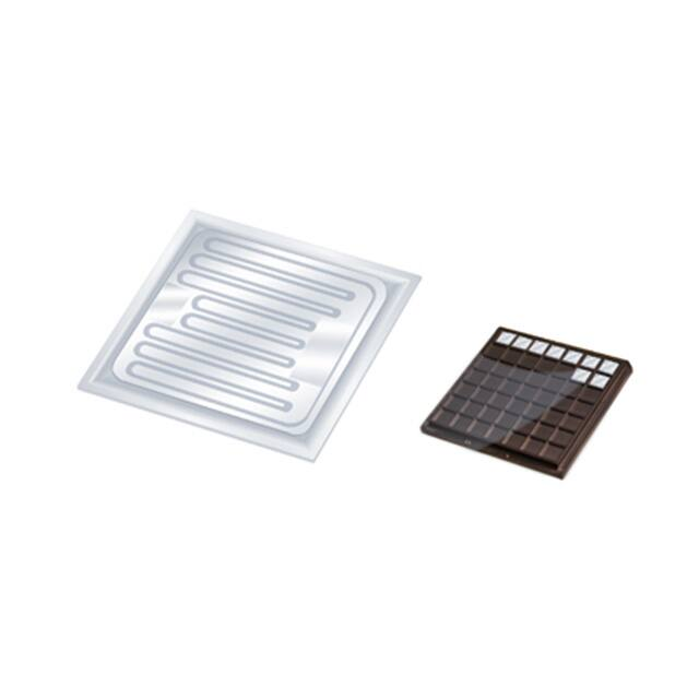


 工商网监
湘ICP备2023018690号
工商网监
湘ICP备2023018690号
