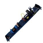
CDB1601-120W
CS1601 120W, High-efficiency PFC
Demonstration Board
Features
General Description
Line Voltage Range: 108 to 305 VACrms
Output Voltage (VLINK): 460V
Rated Pout : 115W
Efficiency: 95% @ 115W
The CDB1601-120W board demonstrates the performance of the CS1601 digital PFC controller as a standalone unit. This board is 95% efficient at full load, and
has been tailored for use with a resonant second stage
to power up to two T5 fluorescent lamps for a maximum
output power of 108W. A resonant second stage driver
efficiency of 94% is assumed for this application.
Spread Spectrum Switching Frequency
Integrated Digital Feedback Control
Low Component Count
ORDERING INFORMATION
CDB1601-120W Customer Demonstration Board
Actual Size:
258 mm x 43 mm
8.16 in x 1.7 in
www.cirrus.com
Copyright Cirrus Logic, Inc. 2011
(All Rights Reserved)
MAR ‘11
DS931DB3
�CDB1601-120W
IMPORTANT SAFETY INSTRUCTIONS
Read and follow all safety instructions prior to using this demonstration board.
7KLV�(QJLQHHULQJ�(YDOXDWLRQ�8QLW�RU�'HPRQVWUDWLRQ�%RDUG� PXVW�RQO\�EH�XVHG�IRU� DVVHVVLQJ�,&� SHUIRUPDQFH�LQ�D�
ODERUDWRU\�VHWWLQJ��7KLV�SURGXFW�LV�QRW�LQWHQGHG�IRU�DQ\�RWKHU�XVH�RU�LQFRUSRUDWLRQ�LQWR�SURGXFWV�IRU�VDOH��
7KLV�SURGXFW�PXVW�RQO\�EH�XVHG�E\�TXDOLILHG�WHFKQLFLDQV�RU�SURIHVVLRQDOV�ZKR�DUH�WUDLQHG�LQ�WKH�VDIHW\�SURFHGXUHV�
DVVRFLDWHG�ZLWK�WKH�XVH�RI�GHPRQVWUDWLRQ�ERDUGV���
�Risk of Electric Shock
•�
7KH�GLUHFW�FRQQHFWLRQ�WR�WKH� $&�SRZHU�OLQH�DQG�WKH� RSHQ�DQG�XQSURWHFWHG�ERDUGV�SUHVHQW�D�VHULRXV�ULVN�RI�HOHFWULF�
VKRFN�DQG�FDQ�FDXVH�VHULRXV�LQMXU\�RU�GHDWK��([WUHPH�FDXWLRQ�QHHGV�WR�EH�H[HUFLVHG�ZKLOH�KDQGOLQJ�WKLV�ERDUG��
•�
$YRLG� FRQWDFW�ZLW K�WK H� H[SRVHG� FRQGXFWRU�R U�WH UPLQDOV� RI� FRPSRQHQWV�R Q�WK H� ERDUG�� +LJK�Y ROWDJH�L V� SUHVHQW�RQ�
H[SRVHG�FRQGXFWRU�DQG�LW�PD\�EH�SUHVHQW�RQ�WHUPLQDOV�RI�DQ\�FRPSRQHQWV�GLUHFWO\�RU�LQGLUHFWO\�FRQQHFWHG�WR�WKH�$&�
OLQH���
•�
'DQJHURXV�YROWDJHV�DQG�RU�FXUUHQWV�PD\�EH�LQWHUQDOO\�JHQHUDWHG�DQG�DFFHVVLEOH�DW�YDULRXV�SRLQWV�DFURVV�WKH�ERDUG��
•�
&KDUJHG�FDSDFLWRUV�VWRUH�KLJK�YROWDJH��HYHQ�DIWHU�WKH�FLUFXLW�KDV�EHHQ�GLVFRQQHFWHG�IURP�WKH�$&�OLQH���
•�
0DNH� VXUH�WK DW�WKH� SRZHU� VRXUFH�L V�RII� EHIRUH�ZL ULQJ� DQ\� FRQQHFWLRQ��0D NH�VX UH�WKDW�DO O� FRQQHFWRUV� DUH� ZHOO�
FRQQHFWHG�EHIRUH�WKH�SRZHU�VRXUFH�LV�RQ��
•�
)ROORZ�DOO�ODERUDWRU\�VDIHW\�SURFHGXUHV�HVWDEOLVKHG�E\�\RXU�HPSOR\HU�DQG�UHOHYDQW�VDIHW\�UHJXODWLRQV�DQG�JXLGHOLQHV��
VXFK�DV�WKH�RQHV�OLVWHG�XQGHU��26+$�*HQHUDO�,QGXVWU\�5HJXODWLRQV���6XESDUW�6�DQG�1)3$���(��
6XLWDEOH�H\H�SURWHFWLRQ�PXVW�EH�ZRUQ�ZKHQ�ZRUNLQJ�ZLWK�RU�DURXQG�GHPRQVWUDWLRQ�ERDUGV��$OZD\V�
FRPSO\�ZLWK�\RXU�HPSOR\HU¶V�SROLFLHV�UHJDUGLQJ�WKH�XVH�RI�SHUVRQDO�SURWHFWLYH�HTXLSPHQW��
$OO�FRPSRQHQWV��KHDW�VLQNV�RU�PHWDOOLF�SDUWV�PD\�EH�H[WUHPHO\�KRW�WR�WRXFK�ZKHQ�HOHFWULFDOO\�DFWLYH��
+HDWVLQNLQJ�LV�UHTXLUHG�IRU�4���7KH�HQG�SURGXFW�VKRXOG�XVH�WDU�SLWFK�RU�DQ�HTXLYDOHQW�FRPSRXQG�IRU�WKLV�
SXUSRVH��)RU�ODE�HYDOXDWLRQ�SXUSRVHV��D�IDQ�LV�UHFRPPHQGHG�WR�SURYLGH�DGHTXDWH�FRROLQJ��
Contacting Cirrus Logic Support
For all product questions and inquiries contact a Cirrus Logic Sales Representative. To find the one nearest to you
go to www.cirrus.com
IMPORTANT NOTICE
Cirrus Logic, Inc. and its subsidiaries ("Cirrus") believe that the information contained in this document is accurate and reliable. However, the information is subject
to change without notice and is provided "AS IS" without warranty of any kind (express or implied). Customers are advised to obtain the latest version of relevant
information to verify, before placing orders, that information being relied on is current and complete. All products are sold subject to the terms and conditions of sale
supplied at the time of order acknowledgment, including those pertaining to warranty, indemnification, and limitation of liability. No responsibility is assumed by Cirrus
for the use of this information, including use of this information as the basis for manufacture or sale of any items, or for infringement of patents or other rights of third
parties. This document is the property of Cirrus and by furnishing this information, Cirrus grants no license, express or implied under any patents, mask work rights,
copyrights, trademarks, trade secrets or other intellectual property rights. Cirrus owns the copyrights associated with the information contained herein and gives
consent for copies to be made of the information only for use within your organization with respect to Cirrus integrated circuits or other products of Cirrus. This consent does not extend to other copying such as copying for general distribution, advertising or promotional purposes, or for creating any work for resale.
CERTAIN APPLICATIONS USING SEMICONDUCTOR PRODUCTS MAY INVOLVE POTENTIAL RISKS OF DEATH, PERSONAL INJURY, OR SEVERE PROPERTY OR ENVIRONMENTAL DAMAGE ("CRITICAL APPLICATIONS"). CIRRUS PRODUCTS ARE NOT DESIGNED, AUTHORIZED OR WARRANTED FOR
USE IN PRODUCTS SURGICALLY IMPLANTED INTO THE BODY, AUTOMOTIVE SAFETY OR SECURITY DEVICES, LIFE SUPPORT PRODUCTS OR OTHER
CRITICAL APPLICATIONS. INCLUSION OF CIRRUS PRODUCTS IN SUCH APPLICATIONS IS UNDERSTOOD TO BE FULLY AT THE CUSTOMER'S RISK
AND CIRRUS DISCLAIMS AND MAKES NO WARRANTY, EXPRESS, STATUTORY OR IMPLIED, INCLUDING THE IMPLIED WARRANTIES OF MERCHANTABILITY AND FITNESS FOR PARTICULAR PURPOSE, WITH REGARD TO ANY CIRRUS PRODUCT THAT IS USED IN SUCH A MANNER. IF THE CUSTOMER
OR CUSTOMER'S CUSTOMER USES OR PERMITS THE USE OF CIRRUS PRODUCTS IN CRITICAL APPLICATIONS, CUSTOMER AGREES, BY SUCH USE,
TO FULLY INDEMNIFY CIRRUS, ITS OFFICERS, DIRECTORS, EMPLOYEES, DISTRIBUTORS AND OTHER AGENTS FROM ANY AND ALL LIABILITY, INCLUDING ATTORNEYS' FEES AND COSTS, THAT MAY RESULT FROM OR ARISE IN CONNECTION WITH THESE USES.
Cirrus Logic, Cirrus, and the Cirrus Logic logo designs are trademarks of Cirrus Logic, Inc. All other brand and product names in this document may be trademarks
or service marks of their respective owners.
2
DS931DB3
�CDB1601-120W
1. INTRODUCTION
The CS1601 is a high-performance Variable Frequency Discontinuous Conduction Mode (VF-DCM), active Power Factor Correction (PFC) controller, optimized to deliver the lowest PFC system cost for electronic ballast applications. The CS1601 uses a digital control algorithm that is optimized for high efficiency
and near unity power factor over a wide input voltage range (108-305 VAC).
The CS1601 uses an adaptive digital control algorithm. Both the ON time and the switching frequency are
varied on a cycle-by-cycle basis over the entire AC line to achieve close to unity power factor. The variation in switching frequency also provides a spread frequency spectrum, thus minimizing the conducted
EMI filtering requirements.
The feedback loop is closed through an integrated digital control system within the IC. Protection features
such as overvoltage, overcurrent, overpower, open circuit, overtemperature, and brownout help protect
the device during abnormal transient conditions. Details of these features are provided in the CS1601 data
sheet.
The CDB1601-120W board demonstrates the performance of the CS1601 over a wide input voltage range
of 108 to 305 VAC, typically seen in universal input ballast applications. This board has been designed
for a 460 V, 115 W full load output application.
Extreme caution needs to be exercised while handling this board. This board is to be powered up by
trained professionals only.
Prior to applying AC power to the CDB1601-120W board, the CS1601 needs to be biased using an external 13 VDC power supply, applied across pins 1 and 3 of terminal block J5. Terminal block J6 is used to
connect the AC line. The load is connected to J7. As a safety measure, jumper J1 is provided as a means
to apply a small resistive load (200 kΩ minium) to rapidly discharge the output capacitors. Other jumpers
and test points are provided to evaluate the behavior of the IC and the various sections of the design.
AC Line
Input
J7
Output
Terminals
J6
J5
VDD Input
J1
Figure 1. Board Connections
DANGER
High Voltage Hazard
ONLY QUALIFIED PERSONNEL SHOULD HANDLE THE CDB1601-120W.
WARNING:
Heatsinking is required for Q4.
The end product should use tar pitch or an equivalent compound for this purpose.
For lab evaluation purposes, a fan is recommended to provide adequate cooling.
DS931DB3
3
�GROUND
NEUTRAL
2
3
CHGND
RV1
S14K300
NO POP
3.15A
SHORT WITH
28 AWG WIRE
C1
2200pF
SHORT WITH 28 AWG WIRE
L5
5mH
NO POP
1. ALL RESISTOR VALUES ARE IN OHMS.
2200pF
C2
C3
NO POP
0.22uF
L1
5mH
2
3
2
NOTES: UNLESS OTHERWISE SPECIFIED;
LINE
1
J6
TERM BLK
F2
1
4
1
4
45 - 65 Hz
2
3
108-305 VAC
1
2
1
3
2
4
C13
0.22uF
L3
1mH
1
4
1
3
2
4
1
-
C4
0.47uF
NO POP
L4
1mH
NO POP
C5
0.33uF
1.15M
R10
1.15M
R12
1.15M
R11
TP6
TP7
D1
1
L2
380uH
MUR160
1
2
3
4
GND
IFB
NC
IAC
CS
0
VDD
GD
GND
ZCD
U1
CS1601-FSZ
R4
R5
17.8K
TP5
8
7
6
5
NO POP
C11
X7R
2200pF
75V
LL4148
GND
R1
24.9
S
R9
0.1
2W
20K
R7
C9
X7R
4.7uF
G
D
MH4
MH3
FD1
1
1
603-00466-Z1
240-00466-Z1
LBL SUBASSY PROD ID AND REV
PCB DWG-
ASSY DWG-
422-00013-01
3057/1 BK005
600-00466-Z1
3050/1 BK005
SCH DWG-
L 500 UL1422 28/1 BLU
1
WIRE-BLACK-INSULATED-16AWG
FD3
WIRE-BLACK-INSULATED-24AWG
4880G
FD2
WIRE-BLUE-INSULATED-28AWG
SCREW-PHILIPS-4-40THR-PH-5/16-L-Z
TO220-INSUL-MOUNT-HEATSINK-KIT
MH2
MH1
2
R18
0.24
1W
COG
33pF
C7
NO POP
3
DESCRIPTION
CHANGED L2 TO NEW FOOTPRINT
INITIAL DESIGN
TP3
2
1
R17
1.78K
R22
0.24
1W
1
2
HS1
12.5W
TP1
R8
0.1
2W
NO POP
SHEET TITLE:
NO POP
DATE:
J3
1K
E3
J7
TERM BLK
115 W
GND
DC LOAD
2
1
3
11/22/2010
G.P. RADHAKRISHNAN
1 OF 1
SHEET
SIZE C
ENGINEER
CDB1601-120W FOR LIGHTING APPLICATIONS
REV C
Buss Bar
E4
J5
TERM BLK
2
1
SHORT WITH 24 AWG WIRE
TP8
Open for efficiency measurements
Jumper for preloading
J1
R20
100K
1W
Resistors for cap discharge
R19
100K
1W
3/21/11
3/21/11
TYPICAL VLINK
460 VDC
1/31/11
COLIN LAMBERT
A. GARZA
12/7/10
G.P. RADHAKRISHNAN
G.P. RADHAKRISHNAN
1/31/11
12/7/10
A. GARZA
A. GARZA
08/10/2010
CHK BY/DATE
G.P. RADHAKRISHNAN
G.MENDEL
08/27/2010
INC BY/DATE
SCHEM., CDB1601-120W
G.P. RADHAKRISHNAN
DRAWN BY:
R3
R2 100
1.15M
R16
1.15M
R15
1.15M
R13
600-00466-Z1
NO POP
C12
X7R
2200pF
R6
0
TP4
C8
COG
330pF
NO POP
C14
ELEC
47uF
250V
C6
ELEC
47uF
250V
GND
DESCRIPTION:
PART #:
C10
COG
100pF
1K
R14
JMP4
0.300" WIRE JUMPER
MURS360T3G
600V
D2
CHGD C13 TO 330V, CHGD WARNING LABEL
ADDED 28AWG, 24AWG & 16AWG WIRES
STF13NM60N
Q4
C
ECO840
1
B
B1
ECO826
A
REV
ECO804
AUXILIARY HARDWARE AND RELATED DOCUMENTS:
2
JMP2
0.750" WIRE JUMPER
Figure 2. Schematic
3
BR1
GBU4J-BP
600V
1
SHORT WITH 28 AWG WIRE
SHORT WITH 16 AWG WIRE
A1
A2
2
12
6
NO POP
L6
4mH
+
10
9
NO POP
L7
4mH
TP2
JMP1
1.15" WIRE JUMPER
FOR USE BY TRAINED PROFESSIONALS ONLY
D4
DANGER: HIGH VOLTAGE
2
1
4
JMP3
0.500" WIRE JUMPER
ECO#
CDB1601-120W
2. SCHEMATIC
DS931DB3
2
�&LUUXV�3�1
070-00157-Z1
011-00042-Z1
011-00055-Z1
011-00040-Z1
013-00034-Z1
012-00186-Z1
001-05280-Z1
001-05783-Z1
001-10233-Z1
001-05542-Z1
001-06276-Z1
011-00064-Z1
070-00132-Z1
070-00166-Z1
070-00001-Z1
180-00022-Z1
311-00019-Z1
115-00014-Z1
110-00301-Z1
110-00302-Z1
080-00013-Z1
050-00039-Z1
050-00050-Z1
040-00127-Z1
040-00127-Z1
050-00039-Z1
050-00047-Z1
304-00004-Z1
071-00107-Z1
020-06337-Z1
020-02502-Z1
020-02616-Z1
020-02273-Z1
020-06390-Z1
020-06310-Z1
030-00091-Z1
030-00091-Z1
020-06356-Z1
020-02616-Z1
020-06391-Z1
020-06372-Z1
030-00080-Z1
036-00015-Z1
110-00045-Z1
065-00331-Z3
080-00002-01
080-00040-Z1
311-00025-Z1
300-00025-Z1
240-00466-Z1
603-00466-Z1
600-00466-Z1
422-00013-01
,WHP
1
2
3
4
5
6
7
8
9
10
11
12
13
14
15
16
17
18
19
20
21
22
23
24
25
26
27
28
29
30
31
32
33
34
35
36
37
38
39
40
41
42
43
44
45
46
47
48
49
50
51
52
53
&,5586�/2*,&
&'%��������:B5HYB&
DS931DB3
A
A
A
A
A
A
A
A
A
A
A
A
A
A
A
A
A2
A
A
A
A
C
C
C
C
A
A
A
A
A
A
A
A
A
A
A
5HY
A
A
A
A
A
A
A
A
A
A
A
A
A
A
A
A
A
TRAN MOSFT nCH 11A 600V NPb TO220FP
RES 24.9 OHM 1/4W ±1% NPb 1206 FILM
RES 100 OHM 1/4W ±1% NPb 1206 FILM
RES 1k OHM 1/4W ±1% NPb 1206 FILM
RES 0 OHM 1/4W NPb 1206 FILM
RES 17.8K OHM 1/4W ±1% NPb 1206
RES 20K OHM 1/4W ±1% NPb 1206 FILM
RES 0.1 OHM 2W ±1% WW NPb AXL
RES 0.1 OHM 2W ±1% WW NPb AXL
RES 1.15M OHM 1/4W ±1% NPb 1206
RES 1k OHM 1/4W ±1% NPb 1206 FILM
RES 1.78K OHM 1/4W ±1% NPb 1206
RES 0.24 OHM 1W ±1% NPb 2512
RES 100K 1W ±5% MTL FLM NPb AXL
VARISTOR 470V RMS 14MM NPb RAD
CON TEST PT .1"CTR TIN PLAT NPb BLK
IC CRUS LPWR FACTOR CORR NPb SOIC8
WIRE 28/1 AWG, KYNAR MOD, 500FT
WIRE 16AWG SOLID PVC INS BLK NPb
HTSNK TO220 MOUNTING KIT NPb
SCREW 4-40X5/16" PH MACH SS NPb
PCB CDB1601-120W-Z-NPb
ASSY DWG CDB1601-120W-Z-NPb
SCHEM CDB1601-120W-Z-NPb
LBL SUBASSY PRODUCT ID AND REV
HDR 2x1 ML .1" 062BD ST GLD NPb TH
CON 3POS TERM BLK 5.08mm SPR NPb RA
CON 2POS TERM BLK 5.08mm SPR NPb RA
WIRE 24 AWG SOLID PVC INS BLK NPb
XFMR 5mH 1:1 1500Vrms 4PIN NPb TH
XFMR 380uH 10% .265O NPb TH
IND 1mH 1.3A ±15% TOR VERT NPb TH
IND 1mH 1.3A ±15% TOR VERT NPb TH
XFMR 5mH 1:1 1500Vrms 4PIN NPb TH
XFMR COMMON MODE CHOKE 1.3 A TH NPb
SPCR STANDOFF 4-40 THR .500"L NPb
'HVFULSWLRQ
DIODE RECT BRIDGE 600V 4A NPb GBU
CAP 2200pF ±10% 2000V CER NPb RAD
CAP 0.22uF ±20% 305V PLY FLM NPb TH
CAP 0.47uF ±20% 305V PLY FLM NPb TH
CAP 0.33uF ±10% 630V POLY NPb RAD
CAP 47UF ±20% 250V ELEC NPb RAD
CAP 33pF ±5% 50V C0G NPb 1206
CAP 330pF ±10% 50V C0G NPb 1206
CAP 4.7uF ±20% 25V X7R NPb 1206
CAP 100pF ±5% 50V C0G NPb 1206
CAP 2200pF ±10% 50V X7R NPb 1206
CAP 0.22uF ±20% 330V PLY FLM NPb TH
DIODE RECT 800V 1A 200mA NPb DO-41
DIODE RECT 600V 4A ULT FST NPb SMC
DIODE SS 75V 500mW NPb SOD80
FUSE 3.15A TLAG IEC NPb SHORT TR5
HTSNK W LOCK TAB .5" TO220 NPb
1
1
1
0
2
1
1
0
1
6
1
1
0
2
0
7
1
2.000
4.000
1
4
1
REF
REF
1
2
2
1
6.000
1
1
1
0
0
0
4
4W\
1
2
0
0
1
2
1
0
1
1
0
1
1
1
1
1
1
Q4
R1
R2
R3
R4 R6
R5
R7
R8
R9
R10 R11 R12 R13 R15 R16
R14
R17
R18 R22
R19 R20
RV1
TP2 TP3 TP4 TP5 TP6 TP7 TP8
U1
W1
W3
XHS1
XMH1MXMH2 XMH3 XMH4
J1 J3
J5 J6
J7
JMP1 JMP2 JMP3 JMP4 W2
L1
L2
L3
L4
L5
L6 L7
MH1 MH2 MH3 MH4
5HIHUHQFH�'HVLJQDWRU
BR1
C1 C2
C3
C4
C5
C6 C14
C7
C8
C9
C10
C11 C12
C13
D1
D2
D4
F2
HS1
ST MICROELECTRONICS
DALE
DALE
DALE
DALE
DALE
DALE
VISHAY
VISHAY
DALE
DALE
DALE
PANASONIC
XICON
EPCOS
KEYSTONE
CIRRUS LOGIC
SQUIRES
ALPHA WIRE COMPANY
AAVID THERMALLOY
BUILDING FASTENERS
CIRRUS LOGIC
CIRRUS LOGIC
CIRRUS LOGIC
CIRRUS LOGIC
SAMTEC
WEIDMULLER
WEIDMULLER
ALPHA WIRE COMPANY
PREMIER MAGNETICS
RENCO
BOURNS
BOURNS
PREMIER MAGNETICS
RENCO
KEYSTONE
0)*
MICRO COMMERCIAL CO
MURATA
EPCOS
EPCOS
PANASONIC
NICHICON
KEMET
KEMET
TDK
KEMET
KEMET
EPCOS
DIODES INC
ON SEMICONDUCTOR
DIODES INC
LITTLE FUSE
AAVID THERMALLOY
%,//�2)�0$7(5,$/��3DJH���RI���
STF13NM60N
CRCW120624R9FKEA
CRCW1206100RFKEA
CRCW12061K00FKEA
CRCW12060000Z0EA
CRCW120617K8FKEA
CRCW120620K0FKEA
G003R1000FE7080
G003R1000FE7080
CRCW12061M15FKEA
CRCW12061K00FKEA
CRCW12061K78FKEA
ERJ1TRQFR24U
294-100K-RC
S14K300
5001
CS1601-FSZ/A2
L 500 UL1422 28/1 BLU
3057/1 BK005
4880G
PMSSS 440 0031 PH
240-00466-Z1
603-00466-Z1
600-00466-Z1
422-00013-01
TSW-102-07-G-S
1716030000
1716020000
3050/1 BK005
TSD-2796
RLCS-1005
2124-V-RC
2124-V-RC
TSD-2796
RL-4400-2-4.00
2203
0)*�3�1
GBU4J-BP
DEBB33D222KA2B
B32923C3224M
B32922C3474M
ECQE6334KF
UVZ2E470MHD
C1206C330J5GAC
C1206C331K5GAC
C3216X7R1E475M
C1206C101J5GAC
C1206C222K5RAC
B32912B3224M
1N4006G-T
MURS360T3G
LL4148
37213150411
6021PBG
ECO840
ADD LENGTH TO BOM QUANTITY IN INCHES
ADD LENGTH TO BOM QUANTITY IN INCHES
INCLUDES ALL MOUNTING HARDWARE
SCREWS FOR STANDOFFS
ECO805/826/840
ECO805/826/840
ECO805/826/840
NO POP
NO POP
NO POP
NO POP
NO POP
NO POP
NO POP
REQUIRES SCREW 4-40X5X16" PH STEEL 300-00025Z1
SEE ASSY DWG FOR LENGTH
REQUIRES 1 SCREW, 300-00025-Z1, 1 WASHER, 30100013-Z1, 1 NUT, 302-00007-Z1 OR MOUNTING KIT
4880G AAVID
NO POP
ECO840
NO POP
NO POP
NO POP
1RWHV
CDB1601-120W
3. BILL OF MATERIALS
5
�6
Figure 5. Silkscreen (Top)
Figure 4. Solder Mask (Top)
Figure 3. Solder Mask (Bottom)
CDB1601-120W
4. BOARD LAYOUT
DS931DB3
�DS931DB3
Figure 8. Silkscreen (Bottom)
Figure 7. Solder Paste Mask (Bottom)
Figure 6. Circuit Routing (Bottom)
CDB1601-120W
7
�CDB1601-120W
5. TYPICAL PERFORMANCE PLOTS
100
277V
230V
95
120V
90
Efficiency (%)
85
80
75
70
65
60
55
50
10
20
30
40
50
60
70
80
90
100
110
120
Output Power (Watts)
Figure 9. Efficiency vs. Output Power
1.00
120V
0.98
230V
0.96
Power Factor
0.94
277V
0.92
0.90
0.88
0.86
0.84
0.82
0.80
20
30
40
50
60
70
80
90
100
110
120
Output Power (Watts)
Figure 10. Power Factor vs. Output Power
8
DS931DB3
�CDB1601-120W
50
45
40
35
THD (%)
30
25
277V
20
15
230V
10
120V
5
0
10
20
30
40
50
60
70
80
90
100
110
120
Output Power (Watts)
Figure 11. THD vs. Output Power
470
468
466
464
Vlink (V)
462
277V
230V
460
120V
458
456
454
452
450
0
10
20
30
40
50
60
70
80
90
100
110
120
Output Power (Watts)
Figure 12. VLink Voltage vs. Output Power
DS931DB3
9
�CDB1601-120W
Figure 13. Steady State Waveforms — 120 VAC
Figure 14. Steady State Waveforms — 230 VAC
10
DS931DB3
�CDB1601-120W
Figure 15. Steady State Waveforms — 277 VAC
DS931DB3
11
�CDB1601-120W
Ch. 1–VLINK
Ch. 2–VRECT
Ch. 3–Gate
Ch. 4–Inductor Current
Figure 16. Switching Frequency Profile at Peak of AC Line Voltage — 120 VAC
Ch. 1–VDS
Ch. 2–VRECT
Ch. 3–CS
Ch. 4–ZCD
Figure 17. Switching Frequency Profile at Peak of AC Line Voltage — 120 VAC (cont.)
12
DS931DB3
�CDB1601-120W
Ch. 1–VLINK
Ch. 2–VRECT
Ch. 3–Gate
Ch. 4–Inductor Current
Figure 18. Switching Frequency Profile at Trough of AC Line Voltage —120 VAC
Ch. 1–VDS
Ch. 2–VRECT
Ch. 3–CS
Ch. 4–ZCD
Figure 19. Switching Frequency Profile at Trough of AC Line Voltage — 120 VAC (cont.)
DS931DB3
13
�CDB1601-120W
Ch. 1–VLINK
Ch. 2–VRECT
Ch. 3–Gate
Ch. 4–Inductor Current
Figure 20. Switching Frequency Profile at Peak of AC Line Voltage — 230 VAC
Ch. 1–VDS
Ch. 2–VRECT
Ch. 3–CS
Ch. 4–ZCD
Figure 21. Switching Frequency Profile at Peak of AC Line Voltage — 230 VAC (cont.)
14
DS931DB3
�CDB1601-120W
Ch. 1–VLINK
Ch. 2–VRECT
Ch. 3–Gate
Ch. 4–Inductor Current
Figure 22. Switching Frequency Profile at Trough of AC Line Voltage — 230 VAC
Ch. 1–VDS
Ch. 2–VRECT
Ch. 3–CS
Ch. 4–ZCD
Figure 23. Switching Frequency Profile at Trough of AC Line Voltage — 230 VAC (cont.)
DS931DB3
15
�CDB1601-120W
Ch. 1–VLINK
Ch. 2–VRECT
Ch. 3–Gate
Ch. 4–Inductor Current
Figure 24. Switching Frequency Profile at Peak of AC Line Voltage — 277 VAC
Ch. 1–VDS
Ch. 2–VRECT
Ch. 3–CS
Ch. 4–ZCD
Figure 25. Switching Frequency Profile at Peak of AC Line Voltage — 277 VAC (cont.)
16
DS931DB3
�CDB1601-120W
Ch. 1–VLINK
Ch. 2–VRECT
Ch. 3–Gate
Ch. 4–Inductor Current
Figure 26. Switching Frequency Profile at Trough of AC Line Voltage — 277 VAC
Ch. 1–VDS
Ch. 2–VRECT
Ch. 3–CS
Ch. 4–ZCD
Figure 27. Switching Frequency Profile at Trough of AC Line Voltage — 277 VAC (cont.)
DS931DB3
17
�CDB1601-120W
Ch. 1–VLINK
Ch. 2–VRECT
Ch. 3–Gate
Ch. 4–Inductor Current
Figure 28. Transient — 15W to 115W Load at 10W/μs, Vin = 120VAC
Ch. 1–VDS
Ch. 2–VRECT
Ch. 3–CS
Ch. 4–ZCD
Figure 29. Transient — 15W to 115W Load at 10W/μs, Vin = 120VAC (cont.)
18
DS931DB3
�CDB1601-120W
Ch. 1–VLINK
Ch. 2–VRECT
Ch. 3–Gate
Ch. 4–Inductor Current
Figure 30. Transient — 15W to 115W Load at 10W/μs, Vin = 230VAC
Ch. 1–VDS
Ch. 2–VRECT
Ch. 3–CS
Ch. 4–ZCD
Figure 31. Transient — 15W to 115W Load at 10W/μs, Vin = 230VAC (cont.)
DS931DB3
19
�CDB1601-120W
Ch. 1–VLINK
Ch. 2–VRECT
Ch. 3–Gate
Ch. 4–Inductor Current
Figure 32. Transient — 15W to 115W Load at 10W/μs, Vin = 277VAC
Ch. 1–VDS
Ch. 2–VRECT
Ch. 3–CS
Ch. 4–ZCD
Figure 33. Transient — 15W to 115W Load at 10W/μs, Vin = 277VAC (cont.)
20
DS931DB3
�CDB1601-120W
Ch. 1–VLINK
Ch. 2–VRECT
Ch. 3–Gate
Ch. 4–Inductor Current
Figure 34. Transient — 115W to Zero Load at 10W/μs, Vin = 120VAC
Ch. 1–VDS
Ch. 2–VRECT
Ch. 3–CS
Ch. 4–ZCD
Figure 35. Transient — 115W to Zero Load at 10W/μs, Vin = 120VAC (cont.)
DS931DB3
21
�CDB1601-120W
Ch. 1–VLINK
Ch. 2–VRECT
Ch. 3–Gate
Ch. 4–Inductor Current
Figure 36. Transient — 115W to Zero Load at 10W/μs, Vin = 230VAC
Ch. 1–VDS
Ch. 2–VRECT
Ch. 3–CS
Ch. 4–ZCD
Figure 37. Transient — 115W to Zero Load at 10W/μs, Vin = 230VAC (cont.)
22
DS931DB3
�CDB1601-120W
Ch. 1–VLINK
Ch. 2–VRECT
Ch. 3–Gate
Ch. 4–Inductor Current
Figure 38. Transient — 115W to Zero Load at 10W/μs, Vin = 277VAC
Ch. 1–VDS
Ch. 2–VRECT
Ch. 3–CS
Ch. 4–ZCD
Figure 39. Transient — 115W to Zero Load at 10W/μs, Vin = 277VAC (cont.)
DS931DB3
23
�CDB1601-120W
6. REVISION HISTORY
Revision
24
Date
Changes
DB1
FEB 2011
Initial Release.
DB2
FEB 2011
Minor BOM change.
DB3
MAR 2011
Updated BOM & Layers to rev C.
DS931DB3
�