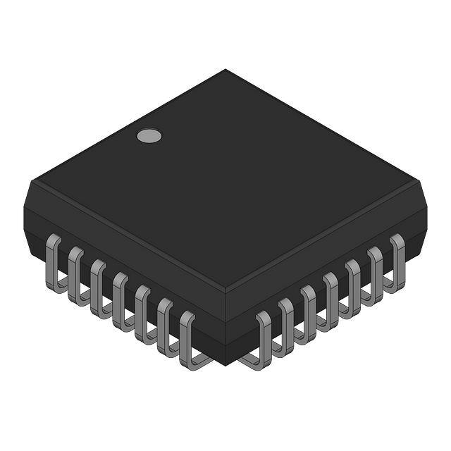
CS61535A
T1/E1 Line Interface
Features
General Description
•
The CS61535A combines the complete analog transmit
and receive line interface for T1 or E1 applications in a
low power, 28-pin device operating from a +5V supply.
Provides Analog PCM Line Interface
for T1 and E1 Applications
• Provides Line Driver, and Data and
Clock Recovery Functions
• Transmit Side Jitter Attenuation
Starting at 6 Hz, with > 300 UI of Jitter
Tolerance
• Low Power Consumption
•
• B8ZS/HDB3/AMI Encoders/Decoders
• 14 dB of Transmitter Return Loss
• Compatible with SONET, M13 , CCITT
G.742, and Other Asynchronous
Muxes
9
RPOS
[RDATA]
RNEG
[BPV]
AMI,
B8ZS,
HDB3
CODER
Interfacing customer premises equipment to a CSU.
Interfacing to E1 links.
Ordering Information
28 Pin Plastic DIP
28 Pin PLCC (j-leads)
(CLKE) (INT) (SDI) (SDO)
MODE TAOS LEN0 LEN1 LEN2
5
28
23
24
TGND
25
CONTROL
PULSE
SHAPER
14
TV+
15
LOOP
BACK
26
TRING
LINE DRIVER
LINE RECEIVER
19 RTIP
20 RRING
SIGNAL
QUALITY
MONITOR
27
RLOOP LLOOP
(CS) (SCLK)
Crystal Semiconductor Corporation
P.O. Box 17847, Austin, TX 78760
(512) 445-7222 FAX: (512) 445-7581
1
12
ACLKI LOS
TTIP
16
CLOCK &
DATA
RECOVERY
7
6
10
JITTER
ATTENUATOR
3
8
•
•
13
2
4
Interfacing network transmission equipment such as
SONET multiplexor and M13 to a DSX-1 cross connect.
CS61535A-IP1
CS61535A-IL1
[ ] = Pin Function in Extended Hardware Mode
( ) = Pin Function in Host Mode
XTALIN XTALOUT
TPOS
[TDATA]
TNEG
[TCODE]
RCLK
Both ICs use a digital Delay-Locked-Loop clock and
data recovery circuit which is continuously calibrated
from a crystal reference to provide excellent stability
and jitter tolerance.
Applications
(typically 175 mW)
TCLK
The device features a transmitter jitter attenuator making it ideal for use in asynchronous multiplexor systems
with gapped transmit clocks. The CS61535A provides a
matched, constant impedance output stage to insure
signal quality on mismatched, poorly terminated lines.
DRIVER
MONITOR
21
22
17 MTIP
[RCODE]
18
MRING
[PCS]
11
DPM
[AIS]
RV+ RGND
Copyright Crystal Semiconductor Corporation 1996
(All Rights Reserved)
MAY ’96
DS40F2
1
�CS61535A
ABSOLUTE MAXIMUM RATINGS
Symbol
Min
Max
Units
RV+
6.0
V
TV+
(RV+) + 0.3
V
Input Voltage, Any Pin
(Note 1)
Vin
RGND-0.3
(RV+) + 0.3
V
Input Current, Any Pin
(Note 2)
Iin
-10
10
mA
Ambient Operating Temperature
TA
-40
85
°C
Storage Temperature
Tstg
-65
150
°C
WARNING:Operations at or beyond these limits may result in permanent damage to the device.
Normal operation is not guaranteed at these extremes.
Notes: 1. Excluding RTIP, RRING, which must stay within -6V to (RV+) + 0.3V.
2. Transient currents of up to 100 mA will not cause SCR latch-up. Also TTIP, TRING, TV+ and TGND
can withstand a continuous current of 100 mA.
DC Supply
Parameter
(referenced to RGND,TGND=0V)
RECOMMENDED OPERATING CONDITIONS
Parameter
Symbol
Min
Typ
Max
Units
DC Supply
(Note 3) RV+, TV+
4.75
5.0
5.25
V
Ambient Operating Temperature
TA
-40
25
85
°C
Power Consumption
(Notes 4, 5)
PC
290
350
mW
Power Consumption
(Notes 4, 6)
PC
175
mW
Notes: 3. TV+ must not exceed RV+ by more than 0.3V.
4. Power consumption while driving line load over operating temperature range. Includes IC and load.
Digital input levels are within 10% of the supply rails and digital outputs are driving a 50 pF load.
5. Assumes 100% ones density and maximum line length at 5.25V.
6. Assumes 50% ones density and 300ft. line length at 5.0V.
2
DS40F2
�CS61535A
DIGITAL CHARACTERISTICS (TA = -40°C to 85°C; TV+, RV+ = 5.0V ±5%; GND = 0V)
Parameter
Symbol
Min
Typ
Max
High-Level Input Voltage
2.0
Pins 1-4, 17, 18, 23-28
(Notes 7, 8, 9)
VIH
Low-Level Input Voltage
Pins 1-4, 17, 18, 23-28
(Notes 7, 8, 9)
VIL
0.8
High-Level Output Voltage (IOUT = -40 µA)
4.0
VOH
Pins 6-8, 11, 12, 25
(Notes 7, 8, 10)
Low-Level Output Voltage (IOUT = 1.6 mA)
0.4
Pins 6-8, 11, 12, 23, 25
(Notes 7, 8, 10)
VOL
Input Leakage Current (Except Pin 5)
±10
Low-Level Input Voltage, Pin 5
VIL
0.2
High-Level Input Voltage, Pin 5
VIH
(RV+) - 0.2
Mid-Level Input Voltage, Pin 5
(Note 11)
VIM
2.3
2.7
Notes: 7. This specification guarantees TTL compatibility (VOH = 2.4V @ IOUT = -40µA).
8. In Host Mode, pin 23 is an open drain output and pin 25 is a tristate output.
9. Pins 17 and 18 of the CS61535A are digital inputs in the Extended Hardware Mode.
10. Output drivers will drive CMOS logic levels into a CMOS load.
11. As an alternative to supplying a 2.3-to-2.7V input, this pin may be left floating.
ANALOG SPECIFICATIONS
Parameter
Units
V
V
V
V
µA
V
V
V
(TA = -40°C to 85°C; TV+, RV+ = 5.0V ±5%; GND = 0V)
Min
Typ
Max
Units
Jitter Attenuator
Jitter Attenuation Curve Corner Frequency
(Note 12)
6
Hz
T1 Jitter Attenuation in Remote Loopback
(Note 13)
Jitter Freq. [Hz]
Amplitude [UIpp]
10
10
3.0
6.0
dB
100
10
20
30
dB
500
10
35
35
dB
1k
5
40
50
dB
10k, 40k
0.3
40
50
dB
E1 Jitter Attenuation in Remote Loopback
(Note 14)
Jitter Freq. [Hz]
Amplitude [UIpp]
10
1.5
3.0
6.0
dB
100
1.5
20
32
dB
400
1.5
30
43
dB
1k
1.5
35
50
dB
10k, 100k
0.2
35
50
dB
Attenuator Input Jitter Tolerance
(Note 15)
12
23
UI
Notes: 12. Not production tested. Parameters guaranteed by design and characterization.
13. Attenuation measured at the demodulator output of an HP3785B with input jitter equal to 3/4 of
measured jitter tolerance using a measurement bandwidth of 1 Hz (10
