w
WM8960
Stereo CODEC with 1W Stereo Class D Speaker Drivers and
Headphone Drivers for Portable Audio Applications
DESCRIPTION
FEATURES
The WM8960 is a low power, high quality stereo CODEC
designed for portable digital audio applications.
Stereo class D speaker drivers provide 1W per channel into 8
loads with a 5V supply. Low leakage, excellent PSRR and
pop/click suppression mechanisms also allow direct battery
connection to the speaker supply. Flexible speaker boost
settings allow speaker output power to be maximised while
minimising other analogue supply currents.
A highly flexible input configuration for up to three stereo
sources is integrated, with a complete microphone interface.
External component requirements are drastically reduced as no
separate microphone, speaker or headphone amplifiers are
required. Advanced on-chip digital signal processing performs
automatic level control for the microphone or line input.
Stereo 24-bit sigma-delta ADCs and DACs are used with low
power over-sampling digital interpolation and decimation filters
and a flexible digital audio interface.
The master clock can be input directly or generated internally by
an onboard PLL, supporting most commonly-used clocking
schemes.
The WM8960 operates at analogue supply voltages down to
2.7V, although the digital supplies can operate at voltages down
to 1.71V to save power. The speaker supply can operate at up
to 5.5V, providing 1W per channel into 8 loads. Unused
functions can be disabled using software control to save power.
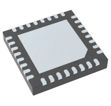
The WM8960 is supplied in a very small and thin 5x5mm QFN
package, ideal for use in hand-held and portable systems.
DGND
DCVDD
DAC SNR 98dB (‘A’ weighted), THD -84dB at 48kHz, 3.3V
ADC SNR 94dB (‘A’ weighted), THD -82dB at 48kHz, 3.3V
Pop and click suppression
3D Enhancement
Stereo Class D Speaker Driver
- 6dB,
3dB steps,
mute
LEFT
MIXER
-12 -> 6dB,
3dB steps,
mute
-17.25 to +30dB,
0.75dB steps
+
vmid
+
-
ADC
0, 13, 20,
29dB,
mute
LINPUT1
INPUT
PGAs
0, 13, 20,
29dB,
mute
RINPUT1
vmid
+
-17.25 to +30dB,
0.75dB steps
+
ADC
DIGITAL
FILTERS
DAC
DIGITAL
FILTERS
ALC
DEEMPHASIS
VOLUME
3D ENHANCE
VOLUME
ADC
RINPUT2
MONO
MIXER
OUT3
0dB / -6dB
DAC
HP_R
-73 to 6dB
1dB steps,
mute
CLASS D
0 to -21dB,
3dB steps
0 to -21dB,
3dB steps
-73 to 6dB
1dB steps,
mute
+BOOST
Jack Detect
PLL
WOLFSON MICROELECTRONICS plc
To receive regular email updates, sign up at http://www.wolfsonmicro.com/enews
MCLK
A-law and u-law support
BCLK
ADCLRC/GPIO1
ADCDAT
DACLRC
DACDAT
VMID
50K
AVDD
AGND
50K
GPIO1
DIGITAL AUDIO
INTERFACE
CONTROL
INTERFACE
SPK_RN
SPK_RP
SPKGND1
SPKGND2
SCLK
SDIN
ADCREF,
DACREF
MICBIAS
SPK_LN
-73 to 6dB
1dB steps,
mute
RIGHT
MIXER
RINPUT3/
JD3
SPK_LP
HP_L
DAC
-12 -> 6dB,
3dB steps,
mute
-12 -> 6dB,
3dB steps,
mute
-73 to 6dB
1dB steps,
mute
+BOOST
Production Data, October 2011, Rev 4.1
Copyright 2011 Wolfson Microelectronics plc
�WM8960
Production Data
TABLE OF CONTENTS
DESCRIPTION ....................................................................................................... 1
FEATURES ............................................................................................................ 1
APPLICATIONS..................................................................................................... 1
TABLE OF CONTENTS ......................................................................................... 2
PIN CONFIGURATION .......................................................................................... 3
ORDERING INFORMATION .................................................................................. 3
PIN DESCRIPTION ................................................................................................ 4
ABSOLUTE MAXIMUM RATINGS ........................................................................ 5
RECOMMENDED OPERATING CONDITIONS ..................................................... 5
ELECTRICAL CHARACTERISTICS ..................................................................... 6
OUTPUT PGA GAIN ............................................................................................ 10
TYPICAL POWER CONSUMPTION.................................................................... 11
SIGNAL TIMING REQUIREMENTS .................................................................... 13
SYSTEM CLOCK TIMING .............................................................................................. 13
AUDIO INTERFACE TIMING – MASTER MODE .......................................................... 13
AUDIO INTERFACE TIMING – SLAVE MODE .............................................................. 14
CONTROL INTERFACE TIMING – 2-WIRE MODE ....................................................... 15
INTERNAL POWER ON RESET CIRCUIT .......................................................... 16
DEVICE DESCRIPTION ...................................................................................... 18
INTRODUCTION ............................................................................................................ 18
INPUT SIGNAL PATH .................................................................................................... 19
ANALOGUE TO DIGITAL CONVERTER (ADC) ............................................................ 26
AUTOMATIC LEVEL CONTROL (ALC) ......................................................................... 28
OUTPUT SIGNAL PATH ................................................................................................ 31
ANALOGUE OUTPUTS ................................................................................................. 37
ENABLING THE OUTPUTS ........................................................................................... 41
HEADPHONE OUTPUT ................................................................................................. 41
CLASS D SPEAKER OUTPUTS .................................................................................... 42
VOLUME UPDATES ...................................................................................................... 43
HEADPHONE JACK DETECT ....................................................................................... 45
THERMAL SHUTDOWN ................................................................................................ 46
GENERAL PURPOSE INPUT/OUTPUT ........................................................................ 47
DIGITAL AUDIO INTERFACE ........................................................................................ 48
AUDIO INTERFACE CONTROL .................................................................................... 52
CLOCKING AND SAMPLE RATES................................................................................ 56
CONTROL INTERFACE................................................................................................. 63
POWER MANAGEMENT ............................................................................................... 63
REGISTER MAP .................................................................................................. 67
REGISTER BITS BY ADDRESS .................................................................................... 68
DIGITAL FILTER CHARACTERISTICS .............................................................. 82
ADC FILTER RESPONSES ........................................................................................... 83
DAC FILTER RESPONSES ........................................................................................... 83
DE-EMPHASIS FILTER RESPONSES .......................................................................... 85
APPLICATIONS INFORMATION ........................................................................ 86
RECOMMENDED EXTERNAL COMPONENTS ............................................................ 86
IMPORTANT NOTICE ......................................................................................... 90
ADDRESS: ..................................................................................................................... 90
REVISION HISTORY ........................................................................................... 91
w
PD, October 2011, Rev 4.1
2
�WM8960
Production Data
PIN CONFIGURATION
32
31
30
29
28
27
26
25
MICBIAS
1
24
SPKGND1
LINPUT3/JD2
2
23
SPK_LN
LINPUT2
3
22
SPK_RP
21
SPKVDD2
20
SPKGND2
LINPUT1
4
RINPUT1
5
RINPUT2
6
19
SPK_RN
RINPUT3/JD3
7
18
SDIN
DCVDD
8
17
SCLK
TOP VIEW
9
10
11
12
13
14
15
16
ORDERING INFORMATION
ORDER CODE
TEMPERATURE RANGE
PACKAGE
MOISTURE
SENSITIVITY LEVEL
PEAK SOLDERING
TEMPERATURE
-40C to +85C
32-lead QFN (5x5x0.9mm)
MSL3
260°C
MSL3
260°C
WM8960CGEFL/V
(Pb-free)
WM8960CGEFL/RV
-40C to +85C
32-lead QFN (5x5x0.9mm)
(Pb-free, Tape and reel)
Note:
Reel quantity = 3500
w
PD, October 2011, Rev 4.1
3
�WM8960
Production Data
PIN DESCRIPTION
PIN NO
NAME
TYPE
1
MICBIAS
Analogue Output
2
LINPUT3 / JD2
Analogue Input
DESCRIPTION
Microphone bias
Left channel line input /
Left channel positive differential MIC input /
Jack detect input pin
3
LINPUT2
Analogue Input
Left channel line input /
Left channel positive differential MIC input
4
LINPUT1
Analogue Input
Left channel single-ended MIC input /
Left channel negative differential MIC input
5
RINPUT1
Analogue Input
Right channel single-ended MIC input /
Right channel negative differential MIC input
6
RINPUT2
Analogue Input
Right channel line input /
Right channel positive differential MIC input
7
RINPUT3 / JD3
Analogue Input
Right channel line input /
Right channel positive differential MIC input /
Jack detect input pin
8
DCVDD
Supply
9
DGND
Supply
Digital core supply
Digital ground (Return path for both DCVDD and DBVDD)
10
DBVDD
Supply
Digital buffer (I/O) supply
11
MCLK
Digital Input
Master clock
12
BCLK
Digital Input / Output
Audio interface bit clock
13
DACLRC
Digital Input / Output
Audio interface DAC left / right clock
14
DACDAT
Digital Input
DAC digital audio data
15
ADCLRC / GPIO1
Digital Input / Output
Audio interface ADC left / right clock / GPIO1 pin
16
ADCDAT
Digital Output
ADC digital audio data
17
SCLK
Digital Input
Control interface clock input
18
SDIN
Digital Input/Output
Control interface data input / 2-wire acknowledge output
19
SPK_RN
Analogue Output
Right speaker negative output
20
SPKGND2
Supply
Ground for speaker drivers 2
21
SPKVDD2
Supply
Supply for speaker drivers 2
22
SPK_RP
Analogue Output
Right speaker positive output
23
SPK_LN
Analogue Output
Left speaker negative output
24
SPKGND1
Supply
Ground for speaker drivers 1
25
SPK_LP
Analogue Output
Left speaker positive output
26
SPKVDD1
Supply
Supply for speaker drivers 1
27
VMID
Analogue Output
Midrail voltage decoupling capacitor
28
AGND
Supply
Analogue ground (Return path for AVDD)
29
HP_R
Analogue Output
Right output (Line or headphone)
30
OUT3
Analogue Output
Mono, left, right or buffered midrail output for capless mode
31
HP_L
Analogue Output
Left output (Line or headphone)
32
AVDD
Supply
33
GND_PADDLE
Analogue supply
Die Paddle (Note 1)
Note:
1.
It is recommended that the QFN ground paddle should be connected to analogue ground on the application PCB.
w
PD, October 2011, Rev 4.1
4
�WM8960
Production Data
ABSOLUTE MAXIMUM RATINGS
Absolute Maximum Ratings are stress ratings only. Permanent damage to the device may be caused by continuously
operating at or beyond these limits. Device functional operating limits and guaranteed performance specifications are given
under Electrical Characteristics at the test conditions specified.
ESD Sensitive Device. This device is manufactured on a CMOS process. It is therefore generically susceptible
to damage from excessive static voltages. Proper ESD precautions must be taken during handling and storage
of this device.
Wolfson tests its package types according to IPC/JEDEC J-STD-020B for Moisture Sensitivity to determine acceptable storage
conditions prior to surface mount assembly. These levels are:
MSL1 = unlimited floor life at 0.546 fs
-50
dB
DAC Sloping Stopband Filter
Passband
+/- 0.03dB
0
0.25 fs
+/- 1dB
0.25 fs
0.454 fs
-6dB
Passband Ripple
0.5 fs
0.25 fs
+/- 0.03
Stopband 1
0.546 fs
Stopband 1 Attenuation
f > 0.546 fs
Stopband 2
-60
dB
0.7 fs
Stopband 2 Attenuation
f > 0.7 fs
Stopband 3
dB
0.7 fs
1.4 fs
-85
dB
1.4 fs
Stopband 3 Attenuation
F > 1.4 fs
DAC FILTERS
Mode
-55
dB
ADC FILTERS
Group Delay
Mode
Group Delay
Normal
18 / fs
Normal
18 / fs
Sloping Stopband
18 / fs
w
PD, October 2011, Rev 4.1
82
�WM8960
Production Data
ADC FILTER RESPONSES
10
3.94
3.84
3.74
3.64
3.54
3.44
3.34
3.24
3.13
3.03
2.93
2.83
2.73
2.63
2.53
2.43
2.33
2.22
2.12
2.02
1.92
1.82
1.72
1.62
1.52
1.42
1.31
1.21
1.11
1.01
0.91
0.81
0.71
0.4
0.61
0.51
0
0.3
0.2
0.1
Magnitude (dB): Passband Ripple
-10
0.1
0.08
-30
0.06
Magnitude (dB)
-50
0.04
-70
0.02
-90
0
0.00
-0.02
-110
0.25
-0.04
-130
-0.06
-150
-0.08
Frequency (fs)
-0.1
Frequency
Figure 38 ADC Digital Filter Frequency Response
Figure 39 ADC Digital Filter Ripple
DAC FILTER RESPONSES
DAC STOPBAND ATTENUATION
The DAC digital filter type is selected by the DACSLOPE register bit as shown in Table 50.
REGISTER
ADDRESS
R6 (06h)
BIT
1
LABEL
DEFAULT
DACSLOPE
0
DESCRIPTION
Selects DAC filter characteristics
ADC and DAC
Control (2)
0 = Normal mode
1 = Sloping stopband mode
Table 50 DAC Filter Selection
MAGNITUDE(dB)
MAGNITUDE(dB)
0.04
10
-10 0
0.5
1
1.5
2
2.5
3
0.035
0.03
-30
0.025
-50
0.02
-70
0.015
-90
0.01
-110
0.005
0
-130
-0.005
-150
Frequency (fs)
Figure 40 DAC Digital Filter Frequency Response (Normal
Mode)
w
0
0.05
0.1
0.15
0.2
0.25
0.3
0.35
0.4
0.45
0.5
Frequency (fs)
Figure 41 DAC Digital Filter Ripple (Normal Mode)
PD, October 2011, Rev 4.1
83
�WM8960
Production Data
MAGNITUDE(dB)
MAGNITUDE(dB)
0.05
10
-10 0
0.5
1
1.5
2
2.5
3
-30
0
-0.05
0
0.05
0.1
0.15
0.2
0.25
0.3
0.35
0.4
0.45
0.5
-0.1
-0.15
-50
-0.2
-70
-0.25
-0.3
-90
-0.35
-110
-0.4
-130
-0.45
-0.5
-150
Frequency (fs)
Figure 42 DAC Digital Filter Frequency Response (Sloping
Stopband Mode)
w
Frequency (fs)
Figure 43 DAC Digital Filter Ripple (Sloping Stopband
Mode)
PD, October 2011, Rev 4.1
84
�WM8960
Production Data
DE-EMPHASIS FILTER RESPONSES
MAGNITUDE(dB)
MAGNITUDE(dB)
0.3
0
-1
0
5000
10000
15000
20000
0.25
0.2
-2
0.15
-3
0.1
-4
0.05
0
-5
-0.05
-6
0
2000
4000
6000
8000
10000
12000
14000
16000
18000
-0.1
-7
-0.15
-8
Frequency (Hz)
-9
-10
Frequency (Hz)
Figure 44 De-Emphasis Digital Filter Response (32kHz)
Figure 45 De-Emphasis Error (32kHz)
MAGNITUDE(dB)
MAGNITUDE(dB)
0.2
0
-1
0
5000
10000
15000
20000
25000
0.15
-2
-3
0.1
-4
0.05
-5
-6
0
-7
0
-8
5000
10000
15000
20000
25000
-0.05
-9
-0.1
-10
Frequency (Hz)
Frequency (Hz)
Figure 46 De-Emphasis Digital Filter Response (44.1kHz)
Figure 47 De-Emphasis Error (44.1kHz)
MAGNITUDE(dB)
MAGNITUDE(dB)
0.15
0
0
5000
10000
15000
20000
25000
30000
-2
0.1
-4
0.05
-6
0
-8
-0.05
-10
-0.1
0
10000
15000
20000
25000
30000
-0.15
-12
Frequency (Hz)
Figure 48 De-Emphasis Digital Filter Response (48kHz)
w
5000
Frequency (Hz)
Figure 49 De-Emphasis Error (48kHz)
PD, October 2011, Rev 4.1
85
�WM8960
Production Data
APPLICATIONS INFORMATION
RECOMMENDED EXTERNAL COMPONENTS
SPEAKER SELECTION
For filterless operation, it is important to select a speaker with appropriate internal inductance. The
internal inductance and the speaker's load resistance create a low-pass filter with a cut-off frequency
of:
fc = RL / 2L
e.g. for an 8 speaker and required cut-off frequency of 20kHz, the speaker should be chosen to
have an inductance of:
L = RL / 2fc = 8 / 2 * 20kHz = 64H
8 speakers typically have an inductance in the range 20H to 100H. Care should be taken to
ensure that the cut-off frequency of the speaker's internal filtering is low enough to prevent speaker
damage. The class D outputs of the WM8960 operate at much higher frequencies than is
recommended for most speakers, and the cut-off frequency of the filter should be low enough to
protect the speaker.
w
PD, October 2011, Rev 4.1
86
�WM8960
Production Data
Figure 50 Speaker Equivalent Circuit
PCB LAYOUT CONSIDERATIONS
The efficiency of the speaker drivers is affected by the series resistance between the WM8960 and
the speaker (e.g. inductor ESR) as shown in Figure 51. This resistance should be as low as possible
to maximise efficiency.
Figure 51 Speaker Connection Losses
The distance between the WM8960 and the speakers should be kept to a minimum to reduce series
resistance, and also to reduce EMI. Further reductions in EMI can be achieved by additional passive
filtering and/or shielding as shown in Figure 52. When additional passive filtering is used, low ESR
components should be chosen to minimise series resistance between the WM8960 and the speaker,
maximising efficiency.
LC passive filtering will usually be effective at reducing EMI at frequencies up to around 30MHz. To
reduce emissions at higher frequencies, ferrite beads placed as close to the device as possible will be
more effective.
Note:
Refer to the application note WAN_0118 on “Guidelines on How to Use QFN Packages and Create Associated PCB
Footprints”
w
PD, October 2011, Rev 4.1
87
�WM8960
Production Data
Figure 52 EMI Reduction Techniques
w
PD, October 2011, Rev 4.1
88
�WM8960
Production Data
PACKAGE DIMENSIONS
FL: 32 PIN QFN PLASTIC PACKAGE 5 X 5 X 0.9 mm BODY, 0.50 mm LEAD PITCH
DM101.A
D
DETAIL 1
D2
32
25
L
1
24
4
EXPOSED
GROUND 6
PADDLE
INDEX AREA
(D/2 X E/2)
E2
17
E
8
2X
16
15
9
b
B
e
1
bbb M C A B
2X
aaa C
aaa C
TOP VIEW
BOTTOM VIEW
ccc C
A3
A
5
0.08 C
C
A1
SIDE VIEW
SEATING PLANE
M
M
45°
DETAIL 2
0.30
EXPOSED
GROUND
PADDLE
DETAIL 1
W
Exposed lead
T
A3
G
H
b
Half etch tie bar
DETAIL 2
Symbols
A
A1
A3
b
D
D2
E
E2
e
G
H
L
T
W
MIN
0.80
0
0.18
3.30
3.30
0.30
Dimensions (mm)
NOM
MAX
NOTE
0.90
1.00
0.02
0.05
0.203 REF
1
0.25
0.30
5.00 BSC
3.45
5.00 BSC
3.45
0.50 BSC
0.20
0.1
0.40
0.103
3.60
2
3.60
2
0.50
0.15
Tolerances of Form and Position
aaa
bbb
ccc
REF:
0.15
0.10
0.10
JEDEC, MO-220, VARIATION VHHD-5.
NOTES:
1. DIMENSION b APPLIES TO METALLIZED TERMINAL AND IS MEASURED BETWEEN 0.15 mm AND 0.30 mm FROM TERMINAL TIP.
2. FALLS WITHIN JEDEC, MO-220, VARIATION VHHD-5.
3. ALL DIMENSIONS ARE IN MILLIMETRES.
4. THE TERMINAL #1 IDENTIFIER AND TERMINAL NUMBERING CONVENTION SHALL CONFORM TO JEDEC 95-1 SPP-002.
5. COPLANARITY APPLIES TO THE EXPOSED HEAT SINK SLUG AS WELL AS THE TERMINALS.
6. REFER TO APPLICATION NOTE WAN_0118 FOR FURTHER INFORMATION REGARDING PCB FOOTPRINTS AND QFN PACKAGE SOLDERING.
7. THIS DRAWING IS SUBJECT TO CHANGE WITHOUT NOTICE.
w
PD, October 2011, Rev 4.1
89
�WM8960
Production Data
IMPORTANT NOTICE
Wolfson Microelectronics plc (“Wolfson”) products and services are sold subject to Wolfson’s terms and conditions of sale,
delivery and payment supplied at the time of order acknowledgement.
Wolfson warrants performance of its products to the specifications in effect at the date of shipment. Wolfson reserves the
right to make changes to its products and specifications or to discontinue any product or service without notice. Customers
should therefore obtain the latest version of relevant information from Wolfson to verify that the information is current.
Testing and other quality control techniques are utilised to the extent Wolfson deems necessary to support its warranty.
Specific testing of all parameters of each device is not necessarily performed unless required by law or regulation.
In order to minimise risks associated with customer applications, the customer must use adequate design and operating
safeguards to minimise inherent or procedural hazards. Wolfson is not liable for applications assistance or customer
product design. The customer is solely responsible for its selection and use of Wolfson products. Wolfson is not liable for
such selection or use nor for use of any circuitry other than circuitry entirely embodied in a Wolfson product.
Wolfson’s products are not intended for use in life support systems, appliances, nuclear systems or systems where
malfunction can reasonably be expected to result in personal injury, death or severe property or environmental damage.
Any use of products by the customer for such purposes is at the customer’s own risk.
Wolfson does not grant any licence (express or implied) under any patent right, copyright, mask work right or other
intellectual property right of Wolfson covering or relating to any combination, machine, or process in which its products or
services might be or are used. Any provision or publication of any third party’s products or services does not constitute
Wolfson’s approval, licence, warranty or endorsement thereof. Any third party trade marks contained in this document
belong to the respective third party owner.
Reproduction of information from Wolfson datasheets is permissible only if reproduction is without alteration and is
accompanied by all associated copyright, proprietary and other notices (including this notice) and conditions. Wolfson is
not liable for any unauthorised alteration of such information or for any reliance placed thereon.
Any representations made, warranties given, and/or liabilities accepted by any person which differ from those contained in
this datasheet or in Wolfson’s standard terms and conditions of sale, delivery and payment are made, given and/or
accepted at that person’s own risk. Wolfson is not liable for any such representations, warranties or liabilities or for any
reliance placed thereon by any person.
ADDRESS:
Wolfson Microelectronics plc
26 Westfield Road
Edinburgh
EH11 2QB
United Kingdom
Tel :: +44 (0)131 272 7000
Fax :: +44 (0)131 272 7001
Email :: sales@wolfsonmicro.com
w
PD, October 2011, Rev 4.1
90
�WM8960
Production Data
REVISION HISTORY
DATE
REV
ORIGINATOR
CHANGES
23/09/11
4.1
JMacD
Order codes changed from WM8960GEFL/V and WM8960GEFL/RV to
WM8960CGEFL/V and WM8960CGEFL/RV to reflect change to copper wire
bonding.
23/09/11
4.1
JMacD
Package Diagram changed to DM101.A.
w
PD, October 2011, Rev 4.1
91
�