PAGE
DATE
NO.
1/10
Messrs.
SPECIFICATION
PRODUCT NAME:
VOLTAGE CONTROLLED CRYSTAL OSCILLATOR
TYPE:
CSX-750V
MHz
FREQUENCY:
PARTS NO.:
CITIZEN WATCH CO., LTD.
1-12, Honcho 6-chome, Tanashi-shi,
Tokyo 188-8511 Japan
Oscillator Technical section
Crystal Devices Div.
Telephone: 0424-68-4572
Fax : 0424-68-4666
PRODUCTS MARKETING GROUP
Telephone: 0424-67-6214
Telex:2822-471/ Fax: 0424-67-8503
APPROVED
CHECKED
PREPARED
�SPECIFICATION
I.
NO.
DATE
PAGE
2/10
SCOPE
This specification relates to the voltage controlled crystal oscillator to be supplied by
CITIZEN WATCH CO., LTD. (following as CITIZEN) to
.
NOTICE
1.If something that is ambiguously defined or undefined in this specification happened,
the customer and CITIZEN would discuss and take necessary steps by mutual consent.
2.Product test data can't be attached to this specification.
3.This product is not authorized for use as critical component in life support devices
or systems.
II. SPECIFICATION
1. ABSOLUTE MAXIMUM RATING
CSX750VB/CSX750VC
Parameter
-0.5V to +7.0V
Supply Voltage
Vmax
Storage Temperature
Tstg
-45°C to +90°C
Output Current
Iout
Input Control Voltage
Vc_m
10mA Max.
-0.5V to Vdd +0.5V
Solder Heat Resistance
Tsol
Max.240°C x Max.10 seconds x 2times
Max.200°C x Max. 3 minutes
Of The Outer Lead
2. OPERATING RANGE
Parameter
CSX750VB
CSX750VC
3.3V±5%
5.0V±10%
Supply Voltage
Vdd
Operating Temperature
Topr
Input Control Voltage
Vc
0.0V to Vdd
Output Load
CL
30pF Max.
-10°C to 70°C or -40°C to 85°C
3. FREQUENCY CHARACTERISTICS
Parameter
CSX750VB
CSX750VC
Stability (note1)
dF0
Pullability (note2)
Fpull
±90ppm Min.
±100ppm Min.
Linearity
Ldev
±15% Max.
±10% Max.
Modulation Band Width
Fmod
±50ppm Max.
10kHz Min.
note1) Frequency Stability includes initial tolerance, temperature characteristics, input
voltage characteristics, load characteristics, shock, vibration, reflow and 1st year aging.
note2) Vc=1.65V±1.65V (CSX750VB) Vc=2.5V±2.0V (CSX750VC)
�SPECIFICATION
NO.
DATE
PAGE
3/10
4. ELECTRICAL CHARACTERISTICS
(Ta=25°C load=30pF Vc=Vdd/2)
Parameter
CSX750VB
Conditions
CSX750VC
4msec Max.
Start Up Time (note)
tosc
Power Supply Current
Idd
No Load
11mA Max.
30mA Max.
Disable Current
Iinh
No Load
5mA Max.
20mA Max.
Rise Time
tr
20% to 80%Vdd
5ns Max.
Fall Time
tf
80% to 20%Vdd
5ns Max.
Duty Cycle
duty
50%Vdd
Output HIGH Voltage
Voh
Ioh = -0.8mA
Output LOW Voltage
Vol
Iol = 3.2mA
OE Input HIGH Voltage
Vih
Vdd x 0.7 Min.
OE Input LOW Voltage
Vil
Vdd x 0.3 Max.
Output Disable Time
tpxz
Output Enable Time
tpzx
45% to 55%
Vdd-0.4V Min.
0.4V Max.
See 5.
100ns Max.
100ns Max.
note) Vc must be kept ground level or left open when starting up.
5. THREE STATE OUTPUT OPERATION
OE Input
Clock Output
HIGH or OPEN
Active
enable
LOW
High impedance
disable
Propagation delay time between
tpxz:OE(HIGH to LOW) and
OUTPUT(active level
to high impedance)
tpxz
Clock
Output
tpzx:OE(LOW to HIGH) and
OUTPUT(high impedance
to active level)
tpzx
high impedance
OE
input
HIGH or OPEN
LOW
NOTE: A disable clock output does not synchronize with OE,
because internal quartz oscillator is continuous.
�SPECIFICATION
NO.
DATE
PAGE
4/10
6. TEST CIRCUIT
[CMOS LOAD] (30pF)
Vdd
[SUPPLY CURRENT]
Vdd
Test Point
6 5
4
Vdd OE OUT
.01 to
0.1uF
Vc
1 2
GND
3
6 5
4
Vdd OE OUT
CL=
30pF
.01 to
0.1uF
1.65V
1.65V
GND
GND
Vc
1
2
[MEASUREMENT CONDITION]
1.Osilloscope
Impedance:No less than 1Mohm
Capacitance:No more than 5pF
Band width:No less than 500MHz
The length of GND lead of the probe should be as short as possible.
2.The CL includes the probe capacitance.
3.Grounding should be single point grounding.
4.Supply impedance should be as low as possible.
0V to 90%Vdd rise time is no less than 150us
5.Use the ammeter that internal impedance is small.
7. OUTPUT WAVEFORM
[CMOS LOAD] (30pF)
tf
tr
80%Vdd
50%Vdd
20%Vdd
Th
T
DUTY=Th/T
GND
3
�SPECIFICATION
NO.
DATE
8. ENVIRONMENTAL AND MECHANICAL CHARACTERISTICS
The following are our reliability test conditions.
Item
Conditions
Shock
MIL-STD-883E 2002.3B
Vibration
MIL-STD-883E 2007.2A
Gross Leak
Leak rate less than 50ppm atm cc /sec of Air
Fine Leak
Leak rate less than 0.01ppm atm cc /sec of Herium
PAGE
5/10
�SPECIFICATION
NO.
DATE
PAGE
6/10
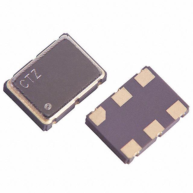
III. DIMENSIONS AND MARKING
(UNIT mm)
Manufucturer's Name
Frequency
CTZ VBBL
32.7680
017105
Type
Production Lot Number
�SPECIFICATION
NO.
DATE
PAGE
7/10
IV. TAPE AND REEL PACKAGING
1. TAPING SPECIFICATION
Subject to EIA 481A & JIS C 0806
(1) Tape Dimensions
Material of the Carrier Tape : PA-PET conductive coat
Material of the Cover Tape : PE A-PET conducutive coat
(2) Reel Dimensions
Material of the Reel : PS
Symbol
Dimension(mm)
A
254+/-2
N
100+/-1
W1
17.5+/-1.0
W2
21.5+/-1.0
�SPECIFICATION
NO.
DATE
(3) Packing
Item
Tape Leader
Tape Trailer
2. INNER CARTON
Cover Tape
Empty Pockets
Cover Tape
Empty Pockets
Empty Space
Min. 500 mm
Min. 20 Pockets
Min. 0 mm
Min. 40 mm
PAGE
8/10
�SPECIFICATION
NO.
DATE
PAGE
9/10
3. OUTER CARTON
4. MARKING
(1) Marking Labels are affixed to reel , inner carton and outer carton.
Reel Marking is consist of:
(2) Each label contains the following information.
* Parts name or type
* Frequency
* Quantity
* Manufucturing Date or symbol
* Manufucturer's name or symbol
* Others(if necessary)
5. QUANTITY
2000 pcs/reel
6. STORAGE ENVIRONMENT
* Storage the reel at normal temperature and humidity
* Open the packing just before using.
* Do not expose the sun.
* Do not storage with some erosive chemicals.
* Nothing is allowed to put on the reel or carton to prevent mechanical damage.
7. HANDLING
* Handle with care to prevent the damege of tape, reel and products.
�SPECIFICATION
NO.
DATE
PAGE
10/10
V. NOTES
1. HANDLING
(ELECTROSTATIC DISCHARGES)
This device is made with CMOS circuitry. Please take precautions
to prevent damage due to electrical static discharge.
(SHOCK RELIABILITY)
This device contains a quartz crystal, so please do not give too much shock or vibration.
An automatic insersion is available, however, the internal quartz crystal might be damaged
in case that too much shock or vibration is given by machine condition. Be sure to check
your machine condition in advance.
(CLEANING)
Since, depending on the cleaning conditions,there is a possibility of damage being caused
to the Crystal Osillator,do not fail to test and confirm the results beforehand,using your
company's cleaning conditions.
(TEMPERATURE AND HUMIDITY)
We recomend to store and use device under normal temperature and humidity.
When this device is used in high humidity applications, there is a potential problem with
condensation.
As with other IC's, please take precautions to prevent condensation.
2. CIRCUIT DESIGNS
(POWER LINES)
We recomend placing a 0.01 to 0.1uF capacitor between VDD and GND to obtain stable
operation and protect against power line ripple .
VDD and GND pattern should be as wide as possible.
(OE INPUT LINE)
When OE pin is not used, please connect it to VDD.
(OUTPUT LINE)
As a long output line may cause irregular output, please take care to design that output line
is as short as possible, and also keep high level signal source away from this device.
(STARTING UP)
Vc must be kept ground level or left open when starting up.
�
CSX750VCB27.000M-UT 价格&库存
很抱歉,暂时无法提供与“CSX750VCB27.000M-UT”相匹配的价格&库存,您可以联系我们找货
免费人工找货