Design Features of C&K Smart Card Connectors
C&K Components has a successful track record of manufacturing innovative interconnect devices with a strong
emphasis on reliability and flexibility. As a long established supplier of such devices for Smart Cards in a wide range
of applications, we have extensive experience matching performance with the need to remain cost sensitive. We
consider the true cost of the interconnect to be a function not just of price, but also the ease with which the device
can be integrated into the customer's production process and its performance in the field. We have built in a number
of features which set our products apart, such as:
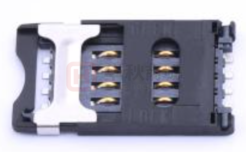
Inlay contact finish
Contact design
A means of applying precious metal to the contact area
utilizing pressure as opposed to conventional plating. We
have found this to be the most durable finish available
without compromising the electrical performance of the
contact. Our research has shown that our inlay finish
lasts over ten times as long as standard gold plating.
Where we state the life of the precious metal this is
intended to be the “worst case” scenario, because the
test has been made using the most abrasive smart card
that we can find on the market (given that the equipment
maker can rarely control which smart cards are used).
Note that the inlay finish is silver in color, being an alloy of
gold, silver, and palladium.
The geometry of the contact has an important bearing on
its electrical performance. Our contacts are designed to
give an efficient wiping action and to maximize the stress
between contact and card, thus minimizing the contact
resistance. The “spooned” contact area is also shaped so
as to protect it from damage during card insertion.
Card detection switches
PCI (security standard for POS applications)
As a manufacturer of switches as well as interconnects,
we have been able to integrate high performance dome
switches into many of our devices. These are variants of
switch products which are already in high volume
production as stand alone components.
Two levels of PCI compatibility level are available:
Mechanical robustness
Materials
Four metal pegs, to be soldered in PCB metalized holes
at the same time than the SMT terminals, have been
designed on the smart card connectors in order to
increase the resistance of the connector to card insertion
force. This participates to the life time and to the overload
resistance.
PCI ready:
Specific features are designed in the connector in order
to ease the integration of security devices around and
below the connector.
PCI:
Additional accessories are integrated on the connector
in order to avoid access to the data contacts and to
detect any connection attempt.
The contact material has been chosen because of its
resistance to atmospheric pollution, solderability and
performance over time in giving a consistent normal
force. Since all of our new interconnects are designed
for surface mounting, the plastic materials used must
withstand high temperature soldering processes without
deforming or adversely affecting performance.
www.ck-components.com
4
�Product Selection Guide
FULL SIZE CARD CONNECTORS
Series
Applications
CCM01
CCM02
CCM04
Professional
Professional
Consumer/Professional
PCI*
PCI ready
EMV
•
40N max
Insertion force
Overload
PCI/PCI ready
•
40N max
250N
180N
Card guide
•
•
Sealed switch
•
•
Operating life
Contact plating
Number of contacts
Contact type
40N
100,000 cycles
500,000 cycles
>50,000 cycles
inlay
inlay
gold
8
8
6 or 8
friction
friction
7
Page No.
10N max
12
friction/vandal proof
17
SIM / SAM CARD CONNECTORS
Series
CCM03
Applications
Cover
Operating life
CCM04
Consumer/Professional
Consumer/Professional
hinged / fixed
hinged / fixed
10,000 to 50,000 cycles
30,000 cycles
•
Sealed switch
Contact plating
inlay / gold
Card end travel switch
with / without
without
6 or 8
6 or 8
24
43
Number of contacts
Page No.
inlay / gold
* PCI
PCI ready: specific features are designed into the connector in order to ease the integration of
security devices around and below the connector.
PCI: specific additional accessories are integrated on the connector in order to avoid acess to the
data contacts and to detect any connection attempt.
Specifications and dimensions subject to change
www.ck-components.com
5
��CCM01 MK2 Series
Features
Typical Applications
• Operating life up to 100,000 cycles
• Transaction
• 40N card insertion force
• Identification
• EMV
• POS
• PCI ready
Mechanical
Contact Electrical Data
Number of Contacts
Mechanical life
Card insertion force
Card extraction force
Contact force
Card detection switch
Insulation resistance
Resistance
Current rating
Dielectric strength
8
Up to 500,000 cycles
40N max.
1 N min / 10 N max
0,2N / 0,50 N max
0,8 N max for actuation (end travel switch
actuation force actuates when card is 0,9mm
from card stop)
1,8 N max for complete depression
Vibration Frequency
10 to 500 Hz. Acceleration 50m/s2
Duration 6 hours - amplitude 0,35mm
Max elect. discontinuity 1µs
Shock
Peak value 500 m/s2 – Duration 11 ms
3 shocks in each direction of each axis
1,000 MΩ min
100 mΩ max
10 µA min / 1 A max
750 Vrms min
Switch Electrical Data
Card detection switch
Contact resistance
Dielectric strength
Current rating
Maximum power
Normally open
100 mΩ max
250 Vrms min
1 mA min / 10 mA max
0.2 VA
Environmental Data
Packaging
Operating temperature
Damp heat
Salt mist
Card detection switch
RoHS compliant
Tray 30 parts / Cartons 300 parts
Reel 200 parts / Cartons 1,000 parts
-40°C to +85°C
IEC 512 test number 11c (10 days)
IEC 512 test number 11f (96 hours)
Sealed against dust
Soldering
Compatible with lead free SMT reflow soldering process
Designation
CCM01-2027LFT
Termination
Operating Life
Card Insertion Force
SMT
100,000 cycles
40N
Dimensions are shown in mm
Specifications and dimensions subject to change
www.ck-components.com
7
Full Size
• Card detection sealed switch
�CCM01 MK2 Series
CCM01-2027 LFT
DETAIL A
Scale 5
0,85
ø 2±0,05
20˚
0,45
2x
A
B
0,7
(7,6)
0,3
2,54
0,1
18,87
10x
A
4
1,2±0,2
3
1
B
4 metal pegs
for 1,6 PCB
51,5
A
A-A
5,85
SEE DETAIL A
Designation & Date-Code area
Card stop
15,5
7,6
B
14
0,9±0,25
9,6
A
20
10
7,6
36,25
A
2027T
XX XX
Pick and place area ø 13
4,15±0,3 Card entry
Card insertion direction
Pad
51,5
SW
2
SW
33,49
29,49
26,49
23,95
18,87
Plastic outline
Contact foot area
1 x 0,7
21,41
RECOMMENDED PC BOARD LAYOUT
(Component side)
0
(2,64)
9,2
9,6
14
Card end travel
switch terminals
0,85 x 0,7
Scale 1
3,81
(55,7)
1,5
8x
C1 C2 C3 C4
0
10
2027T
XX XX
1,5
3,81
15,2
12,9
Full Size
2,1
(9,6)
54,3 Card entry
4,55±0,2
0,7
+0,05
1,05 -0,15 Card entry
55,7±0,1
C5 C6 C7 C8
(50,2)
(36,25)
20
2,1
Contact location according to
ISO/IEC 7816-2
1,3
10x
4x
0,2
ø 0,1
ø 2,2
Metallized
holes
Dimensions are shown in mm
Specifications and dimensions subject to change
www.ck-components.com
8
�Features/Benefits
Typical Applications
• Operating life 500,000 cycles
• Transaction
• Low profile 4 mm and 3.2 mm height
• Identification
• PCI ready
• POS
• Card detection sealed switch
• MPOS
Mechanical
Full Size
CCM01 MK5 Series
Contact Electrical Data
NUMBER OF CONTACTS:
MECHANICAL LIFE:
CARD INSERTION FORCE:
CARD EXTRACTION FORCE:
CONTACT FORCE:
8
500,000 cycles
10 N max.
1 N min. / 10 N max.
0,2 N / 0,60 N max.
1,000 M Ω min.
100 m Ω max.
10 µA min. / 1A max.
750 Vrms min.
INSULATION RESISTANCE:
CONTACT RESISTANCE:
CURRENT RATING:
DIELECTRIC STRENGTH:
Switch Electrical Data
Packaging
CARD DETECTION SWITCH:
CONTACT RESISTANCE:
DIELECTRIC STRENGTH:
CURRENT RATING:
MAXIMUM POWER:
Tray 25 parts or Reel 350 parts
Soldering
Compatible with lead free SMT reflow soldering process
Normally open
100 m Ω max.
250 Vrms min.
1 mA min. / 10 mA max.
0.2 VA
Environmental Data
OPERATING TEMPERATURE: -40˚C to + 85˚C
CARD DETECTION SWITCH: Sealed against dust
RoHS compliant
How To Order
To order, simply select desired option from each category and place in the appropriate box. For additional options not shown in
catalog, consult our Customer Service Center.
C C M 0
1
-
2
L
F
T
Cover Material
Plastic, 4.0 mm height
5
6
Metal, 3.2 mm height
7
Plastic, I/O
NONE
AE
Contact Tail on PCB
Short, recessed (best for PCI)
0
1 Long (accessible, easy rework)
2
Long + 2 metal pegs (40 N overload)
3
Short, no pegs
Leave blank
only applicable with
metal pegs option
(CCM01-2x2x)
Packaging
T25
Pack tray 25 parts
R351
Pack reel 350 parts
Lead Free RoHS
LFT Tin plated termnals
ESD Protection
Full ESD protection (card edge & IC)
3
4
Card edge ESD (only for metal version)
5
Low cost ESD (card edge for plastic cover)
Dimensions are shown in mm
Specifications and dimensions subject to change
www.ck-components.com
9
�CCM01 MK5 Series
CCM01-2604 LFT T25
Metal cover, short tails
DETAIL Q
SCALE 5
A B
5,08
2,54
20
7,6
5,1
2,12
0
SECTION C-C
3,35
15
Card stop
19,5
17,95
17,5
15,65
9,51
9,51
32,1
17,54
SEE DETAIL Q
C5C6C1C2C3C4C7C8 SW1
SW2
10x 1,2
0,2
0,2
9,25
10,81
2x 3
2+0,1
0
0,1
3,8
2x
14,25
B
0
10,81
0,2
1,36
Pick & place area 13
17,85
C
( 32,1 )
8,89
11,43
13,97
16,51
19,05
21,59
24,13
26,67
( 56,25 )
0,2
2x 10
44,45
7,62
43,88
44,45
46,85
49,35
2,54 7x
34,29
8,89
31,75
A
( 56,9 )
0,3
1,9 0,05
1,05 0,1
Card entry
54,2 Card entry
10x 0,7
0,76 0,1
See note 8
C
56,9 0,1
2,35 0,2
Card entry
1,2
CCM01-2513 LFT T25
Plastic cover, long tails, full ESD protection
DETAIL Q
SCALE 5
54,2 Card entry
A B
2,54
20
44,45
7,62
( 56,25 )
C
Pick & place area 13
SECTION C-C
4
SEE DETAIL Q
1
6 ESD
Contacts
7,6
5,1
0,2
( 31,8 )
44,45
46,85
49,35
2,54 7x
8,89
11,43
13,97
16,51
19,05
21,59
24,13
26,67
8,89
0
5,08
A
34,29
0,3
31,75
10x 0,7
( 57 )
1,05 0,1
Card entry
Card stop
19
15,65
9,51
10x 1,2
0,2
0,2
15
17,55
9,51
31,8
18,54
C5C6C1C2C3C4C7C8 SW1
SW2
2x 10
14,25
B
7,5
0
10,81
1,66 0,1
2
0,75 0,1
RECOMMENDED PC BOARD LAYOUT
( component side )
2x 1,5
1,9 0,05
1,65 0,1
2
9,25
10,81
2x
C
57 0,1
2,65 0,2
Card entry
2+0,1
0
0,1
RECOMMENDED PC BOARD LAYOUT
( component side )
Dimensions are shown in mm
Specifications and dimensions subject to change
www.ck-components.com
10
�CCM01 MK5 Series
CCM01-2523 LFT T25
0,1 A B
Plastic cover, long tails, metal pegs
54,2 Card entry
2x
( 57 )
20
C
6 ESD
Contacts
Pick & place area 13
SECTION C-C
4
1
SEE DETAIL Q
( 31,8 )
44,45
46,85
49,35
0,2
38,88
( 56,25 )
44,45
7,62
31,75
2,54 7x
7,6
5,1
8,89
1,3
2,54
8,89
11,43
13,97
16,51
19,05
21,59
24,13
26,67
5,08
A
0
2,88
Full Size
A B
34,29
0,3
1,9 0,05
0,75 0,1
1,66 0,1
1,05 0,1
Card entry
38,88
10x 0,7
DETAIL Q
SCALE 5
2
Card stop
19
15,65
7,5
0
5
7,5
14,25
6x
F
1,5 Metallized holes
0,1
C
D
B
9,25
0,2
0,2
A
E
2x 10
15
17,55
9,51
B
10x 1,2
3,5
3,5
10,81
31,8
18,54
C5C6C1C2C3C4C7C8 SW1
SW2
9,51
39,88
29,88
2,65 0,2
Card entry
57 0,1
2+0,1
0
0,1
8,88
2x
See note 8
C
0
2,88
10,81
RECOMMENDED PC BOARD LAYOUT
( component side )
CCM01-2614 LFT T25
Metal cover, long tails, no ESD protection
DETAIL Q
SCALE 5
54,2 Card entry
( 57 )
A B
2,54
20
C5
C6
C1
14,25
10,81
B
2,35 0,2
Card entry
C2
C3
C4
C7
C8
46,85
49,35
44,45
43,88
34,29
SW1 SW2
10x 1,2
0,2
0,2
2x
9,25
0, 2
9,51
2x 3
2+0,1
0
3, 8
15
17,85
9,51
18,54
32,1
1,2
31,75
19,5
19
17,5
0
57 0,1
21,59
Card stop
15,65
C
19,05
SECTION C-C
3,36
SEE DETAIL Q
0,1
10,81
2x 1,5
2x 10
1,35
Pick & place area 13
7, 6
5,1
2,12
C
( 32,1 )
11,43
( 56,25 )
0,2
16,51
44,45
7,62
13,97
2,54 7x
8,89
8,89
0
5,08
A
26,67
0,3
1 , 9 0 ,0 5
10x 0,7
24,13
1,05 0,1
Card entry
0,75 0,1
1,6 6 0 ,1
2
RECOMMENDED PC BOARD LAYOUT
( component side )
Dimensions are shown in mm
Specifications and dimensions subject to change
www.ck-components.com
11
�CCM02 MK2 Series
Features
Typical Applications
• Operating life 500,000 cycles
• Transaction
• Insertion force 40N
• Identification
• EMV
• POS
• PCI & PCI ready
Full Size
• Card detection sealed switch
Mechanical
Contact Electrical Data
Number of Contacts
Mechanical life
Card insertion force
Card extraction force
Contact force
Card detection switch
Insulation resistance
Resistance
Current rating
Dielectric strength
8
500,000 cycles min
10N to 40N
1N min / 10N max
0,2N / 0,50N max
0,8 N max for actuation (end travel switch
actuation force actuates when card is 0,9mm
from card stop)
1,8 N max for complete depression
Vibration Frequency
10 to 500 Hz. Acceleration 50m/s2
Duration 6 hours - amplitude 0,35mm
Max elect. discontinuity 1µs
Shock
Peak value 500 m/s2 – Duration 11 ms
3 shocks in each direction of each axis
1,000 MΩ min
100 mΩ max
10 µA min / 1 A max
750 Vrms min
Switch Electrical Data
Card detection switch
Contact resistance
Dielectric strength
Current rating
Maximum power
Normally open
100 mΩ max
250 Vrms min
1 mA min / 10 mA max
0.2 VA
Environmental Data
Packaging
Operating temperature
Damp heat
Salt mist
Card detection switch
RoHS compliant
Tray 30 parts / Cartons 300 parts
Reel 120 parts
-40°C to +85°C
IEC 512 test number 11c (10 days)
IEC 512 test number 11f (96 hours)
Sealed against dust
Soldering
Compatible with lead free reflow soldering process
For version with security cover, please contact Customer Service for
soldering recommendations.
PCI Features
Designation
Termination Contact Type I/O Protect Security Cover
Total Height
(mm)
Dimension
PCB version
CCM02-2503LFT
THT
landing
6,25
38,5 X 55,6
4 clips
CCM02-2504LFT
SMT
landing
6,25
38,5 X 55,6
4 clips
CCM02-F503LFT
THT
friction
6,25
38,5 X 55,6
4 clips
CCM02-F504LFT
SMT
friction
6,25
38,5 X 55,6
4 clips
CCM02-F844LFT
SMT
friction
6,6
40,5 X 58
4 metal pegs
Yes
Yes
Dimensions are shown in mm
Specifications and dimensions subject to change
www.ck-components.com
12
�CCM02 MK2 Series
PCI: I/O Protect
Definition
Special accessory in order to avoid and detect frontal access to data contact. It is electrically connected to the
PCB through spring finger contacts.
It must be in open position during the reflow soldering of the connector and has to be locked in closed position
after soldering.
I/O Protect locking tool
C&K is proposing a manual tool to lock the I/O protect accessory after soldering.
Ordering code: C-CM02-E50
PCI: Security Cover
Definition
It is a multilayer cover placed over the connector to avoid and detect data contact access, especially from the top.
It is connected to the PCB through 6 SMT terminals that are soldered at the same time as the other smart card
terminals.
Process
Please contact your Sales Representative for advice and recommendations about soldering this version.
Specifications and dimensions subject to change
www.ck-components.com
13
Full Size
Process
�CCM02 MK2 Series
CCM02-2503 LFT / CCM02-F503 LFT
55,6±0,2
DETAIL A
Scale 5
4,3±0,2
5x
2,54
3,15
19,12
10x
4 Snap
Feet
(3,2)
0,95
6,25
Embossed
Channel
0,3
A B
4x
0,7
ø 0,2
A B
2,9±0,2
52
A
A-A
5,75
Designation & Date-Code area
"CCM02" marking is optional
SEE DETAIL A
Card stop
14
15,7
12,7
B
10
12,7
4 1±0,25
3,2
A
38,5
7,7±0,3
20
F503T
XX XX
A
Card insertion
direction
4,15±0,3 Card entry
52
31,82
29,28
26,74
24,2
21,66
19,12
RECOMMENDED PC BOARD LAYOUT
(Component side)
0
Plastic outline
SW SW
3,2
C1 C2 C3 C4
Card end travel
switch terminals
(55,6)
12,7
10
12,7
0
F503T
XX XX
3,81 3,81
Full Size
1,6 PCB Thickness
0.65
(50)
(38,5)
14
C5 C6 C7 C8
20
1,8
+0,1
ø10
10x
ø 0,1
(4x) ø
3,2
+0,1
0
ø 0,1
Contact location according to
ISO/IEC 7816-2
Dimensions are shown in mm
Specifications and dimensions subject to change
www.ck-components.com
14
�CCM02 MK2 Series
Full Size
CCM02-2504 LFT / CCM02-F504 LFT
Contact location according to ISO 7816-2
Dimensions are shown in mm
Specifications and dimensions subject to change
www.ck-components.com
15
�CCM02 MK2 Series
CCM02-F844A LFT / CCM02-F844B LFT
0,2±0,1
DETAIL B
Scale 5
58±0,3
0,95
4,3±0,2
(5x)
2,54
0,2±0,15
metal peg (4x)
Ø 1,62 ± 0,05
Ø 0.2 A B
51,5
A
A-A
Card stop
6
SEE DETAIL B
10
Labelling : Designation &
Date-Code area
26,35±0,3
B
14
A
15,7
18,87
1±0,25
(14x) 1
16,9
(closed position)
A
20
0,3
1,6 -0,10
Full Size
Embossed
Channel
3,2 +0,4
-0,2
0,8
2,05
0,8
0,7
F844T
xx xx
Contacts security
(closed position)
A
3,6±0,3
Card entry
RECOMMENDED PC BOARD LAYOUT
(Component side)
45º
C5
C6
C7
C8
11,3
38
18,87
21,41
23,95
26,49
29,03
31,57
0
10,5
Contact foot area
Card end travel
switch terminals
38,8
SWSW
P1
P3
3,1 1,7
C1 C2 C3 C4
Scale 1
12,65
11,45
C5 C6 C7 C8
Protection cover
terminals
2
1,5
3,24
20
F844T
xx xx
(6x) 1,3
0,05
P1
Card insertion
direction
P4
P3
(6x) 1,5
0,05
3,81 3,81
P2
0
1,27
(58)
1,27
Plastic
outline
1,3
(50)
(40,5)
Please don't apply any solder
paste on these 4 pads
37,2
9,7
0,2
0
Contact location
according to ISO/IEC 7816-2
P4
1,5
3,81
14
\Piracy
switch \
P2
51,5
metallized holes
(4x)
Ø 1,9
Ø 0,1 A
Dimensions are shown in mm
Specifications and dimensions subject to change
www.ck-components.com
16
�Features
Typical Applications
• ID1 full size card acceptance
• Transaction
• Card detection sealed switch
• POS
• Compatible with pick and place and
lead free soldering
• Identification
Mechanical
Contact Electrical Data
Number of contacts
Mechanical life
Card insertion force
Card extraction force
Contact force
Card detection switch
Insulation resistance
Contact resistance max
Switching current
Dielectric strength
6 or 8
50,000 cycles
10N max
1N min / 10N max
0,4N to 0,7N
0,8 N max for actuation (end travel switch
actuation force actuates when card is 0,9mm
from card stop)
1,8 N max for complete depression
Vibration Frequency
10 to 500 Hz. Acceleration 50m/s2
Duration 6 hours - amplitude 0,35mm
Shock
Peak value 500 m/s2 – Duration 11 ms
3 shocks in each direction of each axis
Max elect. discontinuity 1µs
Full Size
CCM04 MK4 Series
1000 MΩ min
100 mΩ max
10 µA min / 1 A max
750 Vrms min
Switch Electrical Data
Card detection switch
Rc card detection switch
Dielectric strength
Switch current rating
Maximum switch power
Normally open
100 mΩ max
250 Vrms min
1 mA min / 10 mA max
0.2 VA
Environmental Data
Packaging
Operating temperature
Salt mist
Damp heat
Card detection switch
RoHS compliant
See table below
Soldering Process
-40°C to +85°C
IEC 512 test number 11f (96 hours)
IEC 512 test number 11c (10 days)
Sealed against dust
Compatible with lead free SMT reflow soldering process
Designation
Housing Type # of Contacts Contact Force Total Height (mm) Total Dim. (mm)
Packaging
CCM04-5427LFT
standard
8
0,4N to 0,7N
2,65
18,75 X 25
reels of 1,000 pcs
CCM04-5436LFT
standard
8
0,4N to 0,7N
0,90
18,75 X 26,9
reels of 1,000 pcs
CCM04-5468LFT
stand-off
8
0,4N to 0,7N
3,5
18,75 X 24
reels of 1,000 pcs
CCM04-5454LFT
standard
8
0,4N to 0,7N
0,90
18,75 X 26,9
reels of 1,000 pcs
CCM04-5455LFT
standard
8
0,4N to 0,7N
0,90
18,75 X 26,9
reels of 1,000 pcs
Dimensions are shown in mm
Specifications and dimensions subject to change
www.ck-components.com
17
�CCM04 MK4 Series
1,1±0,15
Mated condition
3,81
3,81
40˚0'
DETAIL A
Scale 10
(0,75)
0,5
2,65±0,05
0,25 ± 0,05 x45˚
CCM04-5427 LFT
Full Size
2
11,15
SEE DETAIL A
0,85
2
16,6
0,8
15,15±0,3
9,5±0,3
15,6
B
1,9
0
-0,1
+0,05
-0
0,75±0,15
A
12,9
(15,15)
1,27
2,54
A
0,7
XXXX
(1,97)
8
Top card level recommended
2,54
1,75
2
2x
ø 1,2
1,5 x 45˚
(2,16)
0,3
A
7,65
A
4
45˚0'
4,4
Pick and place area ø 3,3
0,7
R0,
7
3
A
0,1
18,75
7,5
A B
8x
0,3
11,55
1,1±0,05
2,54
7
6
Card stop
0,9±0,25
0,75
+0,10
-0,05
0,6
11,8
15,45
7,8
0,75±0,05
0,8
RECOMMENDED PC BOARD LAYOUT
(Component side)
1,3
13,2
9,2
1,7
C6
C2
C7
C3
C8
C4
(24,65)
SW
(25)
3
1,1
2x
2,54
0,2
8x
0,2
2,54
(11,55)
C1
2,54
C5
1,3
1,3
C
4
Stand-off area
SW
Pad
Contact foot area
0,8 x 0,7
Plastic outline
3,81
3,81
15,15
2,79
Switch contact foot area
0,85 x 0,7
9,5
Contact location according to
ISO/IEC 7816-2
Dimensions are shown in mm
Specifications and dimensions subject to change
www.ck-components.com
18
�CCM04 MK4 Series
CCM04-5436 LFT
DETAIL A
Scale 10
(0,75)
1,1±0,15
0,15
+0,03
-0,07
+0,03
0
2
11,15
1,4
8,5±0,3
15,6
(18,4)
B
0
-0,1
1,9
A
12,9
1,5
0,97
SEE DETAIL A
18,4±0,3
2
+0,05
-0
0,75±0,15
1,27
2,54
7
0,9±0,25
6
2,54
Card stop
Top card level recommended
2,54
1,1±0,05
18,75
8x
0,3
11,55
A
0,7
XXXX
(1,97)
8
3
7,5
Pick and place
area ø 3.3
4
0,7
A
4,4
7,65
45˚0'
A
11,8
7,8
2x
0,3
0,6
1,5 x 45˚
0,75
15,45
(2,16)
R0,7
A
+0,10
-0,05
0,75±0,05
0,8
RECOMMENDED PC BOARD LAYOUT
(Component side)
24,15
C3
(18,75)
A
C7
C8
0,2
+0,1
0
C2
1,3
8x
C1
C6
1,27
C5
11,75
3x 2,54
8,35
+0,1
0
C4
(24)
3,6 x 45˚
SW
(26,9)
11,4
+0,1
0
SW
1,1
2x
7,95
+0,1
0
R0,
2m
in
A
3
18,95
16,4
15,8
4
+0,1
0
1,7
R0,
5 m 10x
ax
8x
+0,1
0
Dimensions are shown in mm
Specifications and dimensions subject to change
www.ck-components.com
19
Full Size
40˚0'
0,5
0,75
+0,10
-0,04
0,25 ± 0,05 x45˚
A-A
Mated condition
3,81
3,81
�CCM04 MK4 Series
CCM04-5468 LFT
40˚
DETAIL A
SCALE 10
3,5±0,08
0,25 ± 0,05 x45˚
2
0,85
15,15±0,3
9,5±0,3
15,6
A
12,9
0,8
0
-0,1
11,15
0,07
Full Size
3,81
0,5
3,81
1,1±0,15
Mated condition
SEE DETAIL A
B
0
-0,1
0,75±0.15
6
1,1±0,05
18,75
2,54
7,5
Top card level recommended
0,3
0,9±0,25
1,27
2,54
7
2,54
A
Card stop
8x
11,55
0,7
XXXX
(1,97)
8
2x
(2,16)
0,3
1,5 x 45˚
4
A
0,7
45˚
4,4
2x
11,8
7,8
0,75
15,45
+0,10
-0,15
0,6
Pick and place area ø 3,3
A
7,65
R0,
7
3
A
0,75±0,05
0,8
RECOMMENDED PC BOARD LAYOUT
(Component side)
13,2
1,3
Stand-off area
6x
Contact foot area
0,8 x 0,7
9,2
1,3
C5
(11,55)
C1
1,3
(18,75)
1,27
C6
C3
C8
(24)
2x
2,54
C7
8x
0,2
2,54
C2
0,2
2,54
1,7
3
1,1
C4
4
SW
SW
Pad
3,81
Plastic outline
Contact location according to
ISO/IEC 7816-2
3,81
2,79
Switch contact foot area
0,85 x 0,7
15,15
9,5
Dimensions are shown in mm
Specifications and dimensions subject to change
www.ck-components.com
20
�CCM04 MK4 Series
(0,75)
0,15
+0,03
-0,07
+0,03
0
2
11,15
1,5
0,97
SEE DETAIL A
18,4±0,3
1,4
8,5±0,3
15,6
(18,4)
B
0
-0,1
2 ±0.05
0,75±0,15
A
12,9
2
Full Size
40˚
DETAIL A
Scale 10
1,1±0,15
Mated condition
3,81
3,81
0,5
0,75
+0,10
-0,04
0,25 ± 0,05 x45˚
CCM04-5454 LFT
1,27
2,54
0,7
XXXX
(1,97)
8
6
Top card level recommended
2,54
7
0,9±0,25
2,54
Card stop
18,75
8x
0,3
11,55
A
1,1±0,05
3
7,5
R0,7
A
4
A
0,7
A
4,4
7,65
45˚
0,3
(2,16)
0,6
1,5 x 45˚
2x
11,8
7,8
0,75
15,45
+0,10
-0,05
0,75±0,05
0,8
1,1
2x
RECOMMENDED PC BOARD LAYOUT
(Component side)
Scale 2,5
2.8±0.05 x 45˚
12.6±0.05
SW
C6
C2
C5
C1
13.2±0.05
0,2
A
R0,5 m
ax
8x
Pick and place area
ø 8 max
(18,75)
C3
1,3
8x
C4
C7
1,27
C8
A
11,75
+0,1
0
3
3x 2,54
18,35
+0,1
0
in
7,35
4
+0,1
0
SW
R1 m
1,7
10x
16,4
8,35
22,9
(24)
+0,1
0
(26,9)
Dimensions are shown in mm
Specifications and dimensions subject to change
www.ck-components.com
21
�CCM04 MK4 Series
Mated condition
(0,75)
3,05
40˚
1,1±0,15
3,81
2,93
3,81
0,5
0,75
+0,10
-0,04
0,25 ± 0,05 x45˚
CCM04-5455 LFT
2
0,97
0,15
+0,03
-0,07
+0,03
0
Full Size
2
SEE DETAIL A
18,4±0,3
11,15
(18,4)
8,5±0,3
15,6
12,9
A
1,4
1,5
B
0
-0,1
2 ±0.05
0,75±0,15
1,27
2,54
0,7
XXXX
(1,97)
8
6
Top card level recommended
7
0,9±0,25
2,54
Card stop
18,75
8x
0,3
2,54
11,55
A
1,1±0.05
3
7,5
R0,7
A
4
A
0,7
A
4,4
7,65
45˚
0,3
(2,16)
0,6
1,5 x 45˚
2x
11,8
7,8
0,75
15,45
+0,10
-0,05
0,75±0,05
0,8
R1 m
SW
3
C6
C2
C5
C1
R0,5 m
ax
8x
(24)
13.2±0.05
0,2
A
Pick and place area
ø 8 max
(18,75)
C3
A
C4
C7
1,27
C8
1,3
8x
11,75
+0,1
0
3x 2,54
18,35
+0,1
0
in
7,35
4
SW
+0,1
0
1,1
2x
RECOMMENDED PC BOARD LAYOUT
(Component side)
Scale 2,5
2.8±0.05 x 45˚
12.6±0.05
1,7
10x
16,4
(26,9)
8,35
22,9
+0,1
0
Dimensions are shown in mm
Specifications and dimensions subject to change
www.ck-components.com
22
��CCM03 MK2 Series
Features
Typical Applications
• SIM/SAM card acceptance
• Handheld products
• Hinged and fixed covers
• Identification
• Compatible with pick and place and
lead free soldering
• POS
• Automotive
Switch Electrical Data
Mechanical
Number of Contacts
Mechanical life, hinged cover
Mechanical life, fixed cover
Card insertion force
Card extraction force
Contact force
Slide locking force
Vibration Frequency
SIM/SAM
Max electrical discontinuity
Shock
6 or 8
10,000 cycles min
50,000 cycles
Hinged cover: 1N max
Fixed cover: 3N max
Hinged cover: 1N max
Fixed cover: 0,80N min / 3N max
0,25N min / 0,50N max
2N min / 6N max
1,8N max. for complete depression
10 to 500 Hz. Acceleration 50m/s2
Duration 6 hours - amplitude 0,35 mm
1µs
Peak value 500 m/s2 – Duration 11 ms
3 shocks in each direction of each axis
Card detection switch
Contact resistance
Dielectric strength
Current rating
Maximum power
Normally open
100 mΩ max
250 Vrms min
1 mA min / 10m A max
0.2 VA
Environment Data
Operating temperature
Damp heat
Salt mist
RoHS compliant
-40°C to +85°C
IEC 512 test number 11c (10 days)
IEC 512 test number 11f (96 hours)
Soldering Process
Compatible with lead free SMT soldering process
Contact Electrical Data
Insulation resistance
Resistance
Current rating
Dielectric strength
Designation
1,000 MΩ min
100 mΩ max
10 µA min / 1 A max
750 Vrms min
Contact Cover
# of
Plating
Contacts
CCM03-3001LFT
inlay
hinged
6
CCM03-3002LFT
inlay
hinged
6
CCM03-3003LFT
inlay
hinged
8
CCM03-3004LFT
inlay
hinged
8
CCM03-3009LFT
gold
hinged
6
CCM03-3010LFT
gold
hinged
6
CCM03-3011LFT
gold
hinged
8
CCM03-3012LFT
gold
hinged
8
CCM03-3013LFT
gold
hinged
6
CCM03-3512LFT
gold
hinged
6
CCM03-3504LFT
gold
fixed
CCM03-3505LFT
gold
CCM03-3754LFT
PCB
Version
Card
Total
Height
Presence Operating
Life
(mm)
Switch
Dim. (mm)
Packaging
without
10,000
2,55
17,2 x 29,65
reels of 1,000 pcs
without
10,000
2,55
17,2 x 29,65
reels of 1,000 pcs
without
10,000
2,55
17,2 x 29,65
reels of 1,000 pcs
without
10,000
2,55
17,2 x 29,65
reels of 1,000 pcs
without
10,000
2,55
17,2 x 29,65
reels of 1,000 pcs
without
10,000
2,55
17,2 x 29,65
reels of 1,000 pcs
without
10,000
2,55
17,2 x 29,65
reels of 1,000 pcs
without
10,000
2,55
17,2 x 29,65
reels of 1,000 pcs
with
10,000
2,55
17,2 x 29,65
reels of 1,000 pcs
without
10,000
2,55
17,2 x 29,65
reels of 1,000 pcs
8
without
50,000
2,85
17,2 x 25,5
reels of 1,000 pcs
fixed
6
without
50,000
2,85
17,2 x 25,5
reels of 1,000 pcs
inlay
fixed
6
with
10,000
3,5
16,5 x 18,05
reels of 1,000 pcs
CCM03-3760LFT
inlay
fixed
6
without
10,000
3,45
16,5 x 15,85
reels of 1,000 pcs
CCM03-3764LFT
inlay
none
6
with
10,000
2,9
16,5 x 15,85
reels of 1,000 pcs
2 plastic pegs
2 plastic pegs
2 plastic pegs
2 plastic pegs
Large soldering pads*
* Can go through reflow upside down
24
�CCM03 MK2 Series
CCM03-3001 LFT / CCM03-3009 LFT
0,4
25,5±0,2
MICROSIM CARD
180?max
(25,5)
5,65±0,2
13,8
2,45 R 1,9
2
1,25
0,8
0,65
3,5
0,1 0-0,1
DETAIL A
Scale 5
29,65
(29,65)
SIM/SAM
SEE DETAIL A
,4
(17,2)
1,3
1,25
25˚
28
Mated condition
3,813,81
0,7
25
,4
±
6x
0,
2
0,3 A
1
3,7
8,6
(2
5)
9,65
A
1,27
2x 2,54
13,15
4
0,
2,55 (2,7 max. includes solder tails)
2,1
Slider locked
(25,5)
(15)
Pick and place area
ø 3,5
17,2
11,25
Bump
XX-XXX
R 1,9
Date Code area
3,81 3,8
RECOMMENDED PC BOARD LAYOUT
(Component side)
1,5
8,6
1,5
5,5 2,5 5,5
1,55
1,8
Pad
C5
C6
C7
Prohibited area
Contact location according to
ENV1375-1 & GSM11-11
0,2
C1
C2
C3
6x
2x 2,54
1,27
23,2
1,3
Plastic outline
Contact foot area
0,8 x 1
3,813,81
9,34
25,5
Dimensions are shown in mm
Specifications and dimensions subject to change
www.ck-components.com
29
�CCM03 MK2 Series
CCM03-3002 LFT / CCM03-3010 LFT
25,5±0,2
B
A
1,27
(2
5)
8,6
180˚max
1
0,7
1,25
(29,65)
0,1 0-0,1
13,8
2,45 R 1,9
28
,
ø 0,1 A B
(25,5)
2
1,25
0,8
0,65
3,5
2x
ø1±0,05
DETAIL A
Scale 5
29,65
5,65±0,2
(17,2)
25˚
4
Mated condition
3,813,81
1,3
0,7
25
,4
6x
20,32
±0
,2
0,3 A
10,16
SEE DETAIL A
SIM/SAM
MICROSIM CARD
9,65
3,7
5,08
10,16
2x 2,54
13,15
4
0,
2,55 (2,7 max. includes solder tails)
2,1
0,4
Slider locked
(25,5)
(15)
Pick and place area
ø 3,5
17,2
11,25
Bump
XX-XXX
R 1,9
Date Code area
3,81 3,8
RECOMMENDED PC BOARD LAYOUT
(Component side)
1,5
23,2
1,5
20,32
Plastic outline
Contact foot area
0,8 x 1
Pad
ø 1,2
1,44
+0,1 2x
0
Contact location according to
ENV1375-1 & GSM11-11
1,3
C1
C2
C3
0,2
2x 2,54
Prohibited area
C5
C6
C7
3,813,81 6,35
9,34
25,5
6x
8,6
1,27
5,08
10,16
1,8
ø 0,1
5,5 2,5 5,5
Dimensions are shown in mm
Specifications and dimensions subject to change
www.ck-components.com
30
�CCM03 MK2 Series
CCM03-3003 LFT
1,27
3x 2,54
MICROSIM CARD
(2
5)
(17,2)
1,3
SEE DETAIL A
13,8
2,45 R 1,9
2
1,25
0,8
0,65
3,5
0,1 0-0,1
DETAIL A
Scale 5
29,65
5,65±0,2
(29,65)
(25,5)
SIM/SAM
1,25
25˚
28
,4
Mated condition
3,813,81
0,7
25
,4
±
8x
0,
2
0,3 A
4
3,7
180?max
0,
1
8,6
9,65
2,55 (2,7 max. includes solder tails)
0,4
13,15
A
25,5±0,2
2,1
Slider locked
(25,5)
(15)
Pick and place area
ø 3,5
17,2
11,25
Bump
XX-XXX
R 1,9
Date Code area
3,81 3,8
RECOMMENDED PC BOARD LAYOUT
(Component side)
1,5
3x 2,54
C5
C6
C7
C8
Prohibited area
Contact location according to
ENV1375-1 & GSM11-11
C1
C2
C3
C4
3,813,81
9,34
1,3
1,8
1,55
0,2
8,6
1,5
5,5 2,5 5,5
Pad
1,27
23,2
8x
Plastic outline
Contact foot area
0,8 x 1
25,5
Dimensions are shown in mm
Specifications and dimensions subject to change
www.ck-components.com
31
�CCM03 MK2 Series
CCM03-3004 LFT
3x 2,54
1
25
,4
±0
,2
0,3 A
2x
(25,5)
0,1 0-0,1
13,8
2
1,25
0,8
0,65
2,45 R 1,9
(29,65)
ø 0,1 A B
DETAIL A
Scale 5
29,65
28
,4
(17,2)
ø1±0,05
0,7
1,25
25˚
3,5
Mated condition
3,813,81
1,3
0,7
5,65±0,2
180˚max
8x
20,32
(2
5)
8,6
9,65
3,7
5,08
10,16
10,16
SEE DETAIL A
Slider locked
(25,5)
(15)
Pick and place area
ø3,5
17,2
11,25
Bump
XX-XXX
R 1,9
Date Code area
3,81 3,8
RECOMMENDED PC BOARD LAYOUT
(Component side)
1,5
Plastic outline
Contact foot area
0,8 x 1
3,813,81 6,35
9,34
25,5
0,2
8x
C1
C2
C3
C4
C5
C6
C7
C8
1,3
1,8
8,6
1,27
1,5
1,44
ø 0,1
5,5 2,5 5,5
3x 2,54
5,08
Prohibited area
Contact location according to
ENV1375-1 & GSM11-11
23,2
20,32
+0,12x
ø 1,2 0
Pad
10,16
SIM/SAM
MICROSIM CARD
4
0,
2,55 (2,7 max. includes solder tails)
13,15
1,27
B
2,1
0,4
A
25,5±0,2
Dimensions are shown in mm
Specifications and dimensions subject to change
www.ck-components.com
28
�CCM03 MK2 Series
CCM03-3011 LFT
A
MICROSIM CARD
(2
5)
9,65
3x 2,54
13,15
13,8
2,45 R 1,9
2
1,25
0,8
0,65
3,5
,4
0,1 0-0,1
DETAIL A
Scale 5
29,65
5,65±0,2
(29,65)
(25,5)
SIM/SAM
SEE DETAIL A
(17,2)
1,3
1,25
25˚
28
Mated condition
3,813,81
0,7
25
,4
±0
8x
,2
0,3 A
3,7
1
180˚ max
4
0,
2,55 (2,7 max. includes solder tails)
2,1
0,4
1,27
25,5±0,2
Slider locked
(25,5)
(15)
Pick and place area
ø 3,5
17,2
11,25
Bump
XX-XXX
Date Code area
3,81 3,8
R 1,9
RECOMMENDED PC BOARD LAYOUT
(Component side)
1,5
5,5
1,5
5,5
Prohibited area
Contact location according to
ENV1375-1 & GSM11-11
3,813,81
9,34
0,2
C1
C2
C3
C4
1,3
1,8
1,55
C5
C6
C7
C8
3x 2,54
1,27
8,6
Pad
23,2
2,5
8x
Plastic outline
Contact foot area
0,8 x 1
25,5
Dimensions are shown in mm
Specifications and dimensions subject to change
www.ck-components.com
29
�CCM03 MK2 Series
CCM03-3012 LFT
3x 2,54
1
180˚max
0,
2
0,3 A
25
,4
±
8x
20,32
(2
8,6
5)
9,65
3,7
5,08
10,16
10,16
0,7
1,25
ø1±0,05
0,1 0-0,1
2
1,25
0,8
0,65
2,45 R 1,9
,4
(25,5)
13,8
3,5
(29,65)
ø 0,1 A B
DETAIL A
Scale 5
29,65
28
2x
(17,2)
25˚
5,65±0,2
Mated condition
3,813,81
1,3
0,7
SEE DETAIL A
Slider locked
(25,5)
(15)
Pick and place area
ø 3,5
17,2
11,25
Bump
XX-XXX
Date Code area
3,81 3,8
R 1,9
RECOMMENDED PC BOARD LAYOUT
(Component side)
1,5
Plastic outline
Contact foot area
0,8 x 1
1,5
1,44
ø0,1
5,5 2,5 5,5
0,2
3x 2,54
3,813,81 6,35
9,34
25,5
8x
C1
C2
C3
C4
C5
C6
C7
C8
1,3
1,8
8,6
1,27
5,08
Prohibited area
Contact location according to
ENV1375-1 & GSM11-11
23,2
20,32
+0,12x
ø 1,2 0
Pad
10,16
SIM/SAM
MICROSIM CARD
4
0,
2,55 (2,7 max. includes solder tails)
13,15
1,27
B
2,1
0,4
A
25,5±0,2
Dimensions are shown in mm
Specifications and dimensions subject to change
www.ck-components.com
30
�CCM03 MK2 Series
CCM03-3013 LFT
0,4
25,5±0,2
2,1
(2
180˚max
(25,5)
13,8
2
1,25
0,8
0,65
2,45 R 1,9
DETAIL
insulated blade switch
Scale 5
SIM/SAM
DETAIL A
Scale 5
29,65
0
0,1 -0,1
SEE DETAIL A
3,5
,4
1,3
1,25
25˚
5,65±0,2
28
Mated condition
3,81 3,81
0,7
25
,
4±
8x
0,
2
0,3 A
4
3,7
1
8,6
5)
9,65
A
1,27
MICROSIM CARD
0,
2,55 (2,7 max. includes solder tails)
3x 2,54
13,15
Slider locked
Plastic actuator
(25,5)
(15)
Pick and place area
ø 3,5
17,2
11,25
XX-XXX
Date Code area
3,81 3,8
R 1,9
RECOMMENDED PC BOARD LAYOUT
(Component side)
1,5
5,5
1,5
5,5
Prohibited area
Contact location according to
ENV1375-1 & GSM11-11
3,813,81
9,34
1,3
(29,65)
0,2
C1
C2
C3
SW
(17,2)
1,8
1,55
C5
C6
C7
SW
3x 2,54
1,27
8,6
Pad
23,2
2,5
8x
Plastic outline
Contact foot area
0,8 x 1
25,5
Dimensions are shown in mm
Specifications and dimensions subject to change
www.ck-components.com
31
�CCM03 MK2 Series
CCM03-3512 LFT
26,9±0,2
(0,3)
A
MICROSIM CARD
(25)
9,65
2x 2,54
13,15
1,27
2,1
180˚max
7,33±0,05
6x
0,3
0,85
1,3
1,25
(17,2)
25˚0'
0,2
4
Mated condition
3,81 3,81
0,7
SEE DETAIL A
(29,65)
(26,9)
DETAIL A
Scale 5
(29,95)
5,65±0,2
0,1
0
-0,1
29,65
13,8
2,45
2
1,25
R 1,9
1,5
0,65
3,5
Slider locked
(26,9)
(15)
Pick and place area
ø 3,5
17,2
11,25
Bump
XX-XXX
3,81
R 1,9
Date Code area
3,8
RECOMMENDED PC BOARD LAYOUT
(Component side)
Plastic outline
1,95
Contact foot area
1,5 x 1
Pad
23,5
1,95
1,4
2,5
5,5
1,3
0,05
C1
C2
C3
3,81
3,81
9,34
6x
8,6
1,8
5,5
C5
C6
C7
2x 2,54
1,27
SIM/SAM
4±
25,
28,
2,55 (2,7 max. includes solder tails)
A
3,7
1
0,4
Prohibited area
Contact location according to
ENV1375-1 & GSM11-11
26,9
Dimensions are shown in mm
Specifications and dimensions subject to change
www.ck-components.com
36
�CCM03 MK2 Series
CCM03-3504 LFT / CCM03-3505 LFT
0,3±0,02
0,3 A
1
8,6
2,54
12,7
12,75
2,5
3x 2,54
1,27
A
10,16
0,4
0,4
DETAIL A
Scale 5
40˚
0,2
Mated condition SEE DETAIL A
3,81 3,81
8x
0,8
2
30˚
25,5
B
Pick and place area
ø 3,5
(25,5)
SIM/SAM
12,1
0,8
0
0,1 -0,1
1,25±0,05
2,65
2,45
2,85 (3 max includes solder tails)
25,5±0,2
0,15 min
Card stop
A
A
1,9
15,2 +0,1
0
17,2±0,05
+0,05
ø 1,4 0
XX-XXX
ø1,6
Date Code area
0,75
2,3
B
1,4 +0,05
0
12,9
21,55
RECOMMENDED PC BOARD LAYOUT
(Component side)
23,2
+0,05
ø 1,4 0
2x
5,5 2,5 5,5
1,5
C3
C8
C4
0,2
C2
C7
1,3
C1
C6
8x
3x 2,54
8,6
1,27
Prohibited area
Contact location according to
ENV1375-1 & GSM11-11
C5
3,81 3,81
(17,2)
2,54
1,44
12,7
1,5
1,8
Plastic outline
Contact foot area
0,8 x 1
Pad
(3,45)
(9,75)
(25,5)
6,35
25,5
Dimensions are shown in mm
Specifications and dimensions subject to change
www.ck-components.com
33
�CCM03 MK2 Series
DETAIL A
A-A
Mated condition
3,81
Date code updated
SEE DETAIL A
3,81
6 F
(16,5)
0
0,1 -0,1
0,4
0,2±0,05
0,25± 0,05 x 45˚
CCM03-3754 LFT
2
2
0,8
3,8±0,2
14,25±0,2
(9,9) (15,85)
0,8
(3,8)
(14,25)
11,8
1,9 +0,05
0
2,54
0,95±0,2
4,9
2,54
(2)
0,3 A
A
3,05
2x
XXXX
Date Code area
6,05
1
A
9,2
15,3
2,54
16,5
0,9±0,25 7
1,27
2,54
8,15
A
0,7
6x
11,1
Card stop
2,5
3,5
0,75 +0,10
-0,05
15,1
RECOMMENDED PC BOARD LAYOUT
(Component side)
Plastic outline
Contact foot area
0,8 x 0,7
Pad
1,5
11,95
3,8
1,5
1,5
8,15
C5
C1
C6
C2
C7
C3
0,2
8x
SW
1,3
1,27
2,54
2,54
2,54
0,075
2,54
SIM/SAM
(4,34)
R1
0,3 A
2,4
1,27
2,4
Pick and place area
ø 3,5
0,85 +0,10
-0,15
0,6
5,9
SW
3,81
Contact location according to
ENV1375-1 & GSM11-11
3,81
Switch contact foot area
0,8 x 1
2,165
5,9
14,25
3,8
Dimensions are shown in mm
Specifications and dimensions subject to change
www.ck-components.com
40
�CCM03 MK2 Series
CCM03-3760 LFT
DETAIL A
SEE DETAIL A
Mated condition
0,2±0,05
3,81
3,81
0,1
0
-0,1
(16,5)
0,4
0,25 ± 0,05 x 45˚
COUPE A-A
2
(9,9)
(15,85)
0,8
(14,25)
14,25±0,2
11,8
5,9
1,9
2,4
0,75
2,4
0,6
Pick and place area
+0,05
0
A
ø 3,5
1,27
8,15
2,54
A
0,7
11,1
6x
0,3
(4,34)
R1
1,27
SIM/SAM
15,3
2,54
16,5
Card stop
6,05
(7,08)
A
A
2,5
XXXX
4,9
Date Code area
3,05
9,2
0,75
15,1
+0,10
-0,05
RECOMMENDED PC BOARD LAYOUT
(Component side)
Plastic outline
Contact foot area
0,8 x 0,7
1,5
11,95
1,5
Pad
C5
C1
C6
C2
C7
C3
1,27
6x
2,54
0,2
1,3
2,54
8,15
0,075
3,81
Contact location according to
ENV1375-1 & GSM11-11
3,81
2,165
5,9
14,25
Dimensions are shown in mm
Specifications and dimensions subject to change
www.ck-components.com
41
�CCM03 MK2 Series
0,25 ± 0,05 x 45˚
CCM03-3764 LFT
SEE DETAIL A
Mated condition
3,81
6
F
2
2
0,8
14,25±0,2
(16,5)
0,1
0
-0,1
3,81
0,8
(14,25)
3,8±0,2
(9,9)
(3,8)
(15,85)
11,8
5,9
1,9
+0,05
0
0,75
0,6
Pick and place area
1,27
9,2
2x
4,9
Date Code area
(2)
0,3
A
15,3
Top card level recommended
2,54
A
6,05
1
A
1,27
2,54
0,95±0,2
XXXX
+0,1
0
A
7
2,54
16,5
0,9 ±0,25
2,5
0,75
15,1
2,9
+0,10
-0,05
RECOMMENDED PC BOARD LAYOUT
(Component side)
Plastic outline
Contact foot area
0,8 x 0,7
1,5
11,95
1,5
3,8
1,5
Pad
C5
C1
C6
C2
C7
C3
0,2
SW
1,3
8x
1,27
2,54
2,54
2,54
8,15
0,075
2,54
SIM/SAM
0,95
2,54
Card stop
0,7
11,1
6x
8,15
0,3
(4,34)
A
ø 3,5
SW
3,81
Contact location according to
ENV1375-1 & GSM11-11
3,81
Switch contact foot area
0,8 x 1
2,165
5,9
14,25
3,8
Dimensions are shown in mm
Specifications and dimensions subject to change
www.ck-components.com
42
�CCM04 MK3 Series
Features
Typical Applications
• SIM and SAM card acceptance
• Mobile
• Compatible with pick and place and
lead free soldering
• POS
• Identification
• GPS
Mechanical
Contact Electrical Data
6 or 8
30,000 cycles
10N max
1N min / 10N max
0,35N min to 0,65N
10 to 500 Hz. Acceleration 50m/s2
Duration 6 hours - amplitude 0,35mm
Shock
Peak value 500 m/s2 – Duration 11 ms
3 shocks in each direction of each axis
Max elect. discontinuity 1µs
Insulation resistance
Contact resistance max
Switching current
Dielectric strength
Number of contacts
Mechanical life
Card insertion force
Card extraction force
Contact force
Vibration Frequency
1000 MΩ min
100 mΩ max
10 µA min / 1 A max
750 Vrms min
Environmental Data
Operating temperature
Salt mist
Damp heat
RoHS compliant
-40°C to +85°C
IEC 512 test number 11f (96 hours)
IEC 512 test number 11c (10 days)
Packaging
SIM/SAM
See table below
Soldering Process
Compatible with lead free SMT soldering process
Designation
CCM04-5137LFS
# of Contacts
Contact Plating
PCB Version
Height (mm)
Dim. (mm)
Packaging
6
gold
SMT IN
1,9
8,15 X 10,45
reels of 1,900 pcs
Dimensions are shown in mm
Specifications and dimensions subject to change
www.ck-components.com
43
�CCM04 MK3 Series
CCM04-5137 LFS
0,75
A
1,9
+0,05
0
(11,8)
0,25 ± 0,05 x 45˚
(1,27)
6x
0,3
2,54
A
7,62
0,7
2,54
(7,62)
(1,27)
11,8
Mated condition
3,81
3,81
SEE DETAIL A
Z
DETAIL A
Scale 10
2
0,6
Date Code area
(10,45)
2,54
2,54
XX
XXX
25
R0,
Pick and place area
ø 3,3
RECOMMENDED PC BOARD LAYOUT
(Component side)
Plastic outline
Contact foot area
0,6 x 0,7
1,5
8,15
1,5
Pad
C1
C6
C2
C7
C3
1
2,54
C5
6x
0,2
2,54
SIM/SAM
0,1
0
-0,1
10,45±0,2
Contact location according to
ISO 7816-2 & ENV 1375-1 & GSM11-11
3,81
3,81
0,265
10,45
Dimensions are shown in mm
Specifications and dimensions subject to change
www.ck-components.com
46
�