CPC1017N
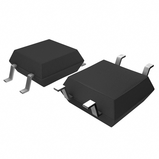
4 Pin SOP OptoMOS® Relays
Load Voltage Load Current Max RON Current to operate
CPC1017N 60 100 16 1.0
Units V mA Ω mA
Applications • Security • Passive Infrared Detectors (PIR) • Data Signalling • Sensor Circuitry • Instrumentation • Multiplexers • Data Acquisition • Electronic Switching • I/O Subsystems • Meters (Watt-Hour, Water, Gas) • Medical Equipment—Patient/Equipment Isolation • Aerospace • Industrial Controls
PR EL IM IN A RY
Approvals • UL Recognized Component • BSI Certified to EN60950 Ordering Information
Part # CPC1017N CPC1017NTR Description 4 Pin SOP (100/tube) 4 Pin SOP (2,000/reel)
Features • Design for use in security systems complying with EN50130-4 • Only 1mA of LED curent required to operate • Small 4 Pin SOP Package • TTL/CMOS Compatible input • No Moving Parts • High Reliability • Arc-Free With No Snubbing Circuits • 1500VRMS Input/Output Isolation/2100V AC peak • No EMI/RFI Generation • Immune to radiated EM fields • SMD Pick & Place, Wave Solderable • Tape & Reel Version Available
Description The CPC1017N is a miniature 1-Form-A solid state relay in a 4 pin SOP package that employs optically coupled MOSFET technology to provide 1500V of input to output isolation. The super efficient MOSFET switches and photovoltaic die use Clare’s patented OptoMOS architecture. The optically coupled input is controlled by a highly efficient GaAIAs infrared LED. The CPC1017N uses Clare’s state-of-the-art double molded vertical construction packaging to produce the world’s smallest relay. The CPC1017N offers board space savings of at least 20% over the competitor’s larger 4 pin SOP relay. It boasts the industries’ lowest input current to operate in its class.
Pin Configuration
CPC1017N Pinout
+ Control
1
4
Load
– Control
2
3
Load
Switching Characteristics of Normally Open (Form A) Devices
10ms CONTROL LOAD 10%+ +90% TON 10%+ TOFF
DS-CPC1017N-R0A.1
www.clare.com
1
�CPC1017N
Absolute Maximum Ratings (@ 25˚ C)
Parameter Input Power Dissipation Input Control Current Peak (10ms) Reverse Input Voltage Total Power Dissipation Isolation Voltage Input to Output(AC Peak test voltage) Operational Temperature Storage Temperature Soldering Temperature (10 Seconds Max.)
1
Min 2100 -40 -40 -
Typ Max Units 70 50 1 5 4001 mW mA A V mW
Absolute Maximum Ratings are stress ratings. Stresses in excess of these ratings can cause permanent damage to the device. Functional operation of the device at these or any other conditions beyond those indicated in the operational sections of this data sheet is not implied. Exposure of the device to the absolute maximum ratings for an extended period may degrade the device and effect its reliability.
Vpeak °C +85 +125 °C +220 °C
Derate Linearly 3.33 mw / oC
Electrical Characteristics
Parameter
Output Characteristics @ Load Voltage (Peak) Load Current (Continuous) AC Peak 1 Peak Load Current On-Resistance 2 Off-State Leakage Current Switching Speeds Turn-On Turn-Off Output Capacitance Capacitance Input to Output Input Characteristics @ 25°C Input Control Current 3 Input Dropout Current Input Voltage Drop Reverse Input Voltage Reverse Input Current
1Load 2
current derates linearly from 100mA @ 25oC to 80mA @ 80oC. Measurement taken within 1 second of on time. 3 For applications requiring high temperature operation (greater than 60oC) an LED drive current of 3mA is recommended.
PR EL IM IN A RY
Conditions IL=1µA Symbol VL Min Typ Max 60 25°C V IF=10mA 10ms IL=100mA VL=60V IL ILPK RON ILEAK 100 350 16 1 10 10 IF=5mA, VL=10V IF=5mA, VL=10V 50V; f=1MHz TON TOFF COUT 25 1 IL=150mA IF=5mA VR=5V IF IF VF VR IR 1 0.3 0.9 0.9 1.2 50 1.4 5 10
Units
mA mA Ω µA ms ms pF pF
mA mA V V µA
2
www.clare.com
R0A.1
�CPC1017N
PERFORMANCE DATA*
CPC1017N Typical LED Forward Voltage Drop (Ambient Temperature = 25oC) IF = 5mADC CPC1017N Typical On-Resistance Distribution (Ambient Temperature = 25 C) (Load Current = 100mA)
o
CPC1017N Typical IF for Switch Operation (Ambient Temperature = 25oC) (Load Current = 100mA)
25 20 15 10 5 0
35 30 Device Count (N) 25 20 15 10 5 0
35 30
Device Count (N)
25 20 15 10 5
PR EL IM IN A RY
0
Device Count (N)
1.17
1.19
1.21
1.23
1.25
6.8
6.9
7.0
7.1
7.2
7.3
7.4
0.30
0.35
0.40
0.45
0.50
0.55
0.60
LED Forward Voltage Drop (V)
On-Resistance (Ω)
LED Current (mA)
CPC1017N Typical IF for Switch Dropout o (Ambient Temperature = 25 C) (Load Current = 100mA)
25 20 15 10 5 0
25 20 15 10 5 0
CPC1017N Typical Turn-On Time (Ambient Temperature = 25oC) (Load Current = 100mA; IF = 5mA)
25 20 15 10 5 0
CPC1017N Typical Turn-Off Time (Ambient Temperature = 25oC) (Load Current = 100mA; IF = 5mA)
Device Count (N)
Device Count (N)
Device Count (N)
0.30
0.35
0.40
0.45
0.50
0.55
0.60
1.0
1.1
1.2
1.3
1.4
1.5
1.6
0.26
0.28
0.30
0.32
0.34
0.36
0.38
LED Current (mA)
Turn-On (ms)
Turn-Off (ms)
CPC1017N Typical Load Current vs. Temperature
180 160 Load Current (mA) 140 120 100 80 60 40 20 0
0.016 0.014 0.012 0.010 0.008 0.006 0.004 0.002
CPC1017N Typical Leakage vs. Temperature (Measured across Pins 3 & 4) IL = max rated
CPC1017N Typical Turn-On vs. Temperature (Load Current = 50mA)
IF =5mA IF =2mA
-40
-20
0
20
40
60
80
100
120
0
5.000 4.500 4.000 3.500 3.000 2.500 2.000 1.500 1.000 0.500 0
Leakage (µA)
Turn-On (ms)
IF =2mA IF =5mA
-40
-20
0
20
40
60
80
100
-40
-20
0
20
40
60
80
100
Temperature ( C)
o
Temperature (oC)
Temperature (oC)
CPC1017N Typical Turn-Off vs. Temperature (Load Current = 50mA)
CPC1017N Typical Turn-Off vs. Temperature (Load Current = 50mA)
CPC1017N Typical LED Forward Voltage Drop vs. Temperature
1.000 0.900 0.800 0.700 0.600 0.500 0.400 0.300 0.200 0.100 0 -40 -20 0 20 40 60 Temperature ( oC)
IF =5mA
IF =2mA
80 100
1.000 0.900 0.800 0.700 0.600 0.500 0.400 0.300 0.200 0.100 0 -40 -20 0 20 40
o
LED Forward Voltage Drop (V)
1.8 1.6 1.4 1.2 1.0 0.8 -40 -20 0 20 40 60 80 100 120 Temperature (oC)
Turn-Off (ms)
Turn-Off (ms)
50mA 10mA 5mA
IF =5mA
IF =2mA
60 80 100 Temperature ( C)
* The Performance data shown in the graphs above is typical of device performance. For guaranteed parameters not indicated in the written specifications, please contact our application department. R0A.1
www.clare.com
3
�CPC1017N
PERFORMANCE DATA*
CPC1017N Typical Turn-On vs. LED Forward Current (Load Current = 100mA; IF=5mA)
3.0 2.7 2.4 2.1 1.8 1.5 1.2 0.9 0.6 0.3 0 0 5 10 15 20 25 30 35 40 45 50 LED Forward Current (mA)
CPC1017N Typical Turn-Off vs. LED Forward Current (Load Current = 100mA)
0.7 0.6 Turn-Off (ms) 0.5 0.4 0.3 0.2 0.1 0 0 5 10 15 20 25 30 35 40 45 50 LED Forward Current (mA) On-Resistance ( )
60 50 40 30 20 10 0
CPC1017N Typical On-Resistance vs. Temperature (Load Current = 50mA; IF = 5mA)
Turn-On (ms)
-40
-20
0
20
40
60
80
100
Temperature (oC)
CPC1017N Typical IF for Switch Operation vs. Temperature (Load Current = 50mA)
3.000 2.500 LED Current (mA) 2.000 1.500 1.000 0.500 0 -40
-20
PR EL IM IN A RY
150 100 50
CPC1017N Typical Load Current vs. Load Voltage (Ambient Temperature = 25oC) IF = 5mA
CPC1017N Energy Rating Curve
0
-50
-100 -150
0
20
40
60
80
100
-3
-2
-1
0
1
2
3
1.0 0.9 0.8 0.7 0.6 0.5 0.4 0.3 0.2 0.1 0 10µs 100µs 1ms 10ms 100ms Time
Load Current (mA)
Load Current (A)
1s
10s 100s
Temperature ( C)
o
Load Voltage (V)
* The Performance data shown in the graphs above is typical of device performance. For guaranteed parameters not indicated in the written specifications, please contact our application department.
4
www.clare.com
R0A.1
�CPC1017N
MECHANICAL DIMENSIONS
4 Pin SOIC Narrow (“N” Suffix)
.38 TYP. (.015 TYP.)
6.096 ± .102 (.240 ± .004) .38 x 45¼ (.015 x 45¼ )
3.81 ± .08 (.150 ± .003)
.432 ± .127 (.017 ± .005)
PC Board Pattern (Top View)
2.54 ± 0.127 (0.100 ± 0.005)
Tape and Reel Packaging for 4 pin SOIC package
330.2 DiA (13.00")
PR EL IM IN A RY
.20 ± .025 (.008 ± .001) 2.54 TYP. (.100 TYP.)
1.02 ± .025 (.040 ± .001)
2.16 MAX. (.085)
4.09 ± 0.20 (0.161 ± 0.008)
1.448 (0.057)
5.66 ± 0.14 (0.223 ± 0.005)
0.889 (0.035)
_ 6.50+ 0.15 4.2
8.00
3.0 R
A
1.5 dia
_ 2.30 + 0.15 .3 R MAX TYP
Top Cover Tape Thickness 3.8 0.102 MAX _ 4.70 + 0.15 TYP (0.004)
12.00 _ 5.50 + .10
1.50 1.60
A
_ 2.00 + .05 _ 4.00 + .10
1.75
.30 _ 2.7 + 0.15 SECTION A-A
Embossed Carrier
Embossment
Dimensions mm (inches)
R0A.1
www.clare.com
5
�For additional information please visit our website at: www.clare.com
Clare, Inc. makes no representations or warranties with respect to the accuracy or completeness of the contents of this publication and reserves the right to make changes to specifications and product descriptions at any time without notice. Neither circuit patent licenses nor indemnity are expressed or implied. Except as set forth in Clare’s Standard Terms and Conditions of Sale, Clare, Inc. assumes no liability whatsoever, and disclaims any express or implied warranty, relating to its products including, but not limited to, the implied warranty of merchantability, fitness for a particular purpose, or infringement of any intellectual property right. The products described in this document are not designed, intended, authorized or warranted for use as components in systems intended for surgical implant into the body, or in other applications intended to support or sustain life, or where malfunction of Clare’s product may result in direct physical harm, injury, or death to a person or severe property or environmental damage. Clare, Inc. reserves the right to discontinue or make changes to its products at any time without notice. Specification: DS-CPC1017N-R0A.1 ©Copyright 2001, Clare, Inc. OptoMOS® is a registered trademark of Clare, Inc. All rights reserved. Printed in USA. 10/8/01
�
很抱歉,暂时无法提供与“CPC1017N”相匹配的价格&库存,您可以联系我们找货
免费人工找货