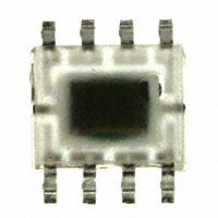
CPC1822
4V Output Solar Cell
Parameter Open Circuit Voltage Short Circuit Current
Rating 4 50
Units V uA
Description
The CPC1822 is a monolithic photovoltaic string of solar cells with switching circuitry. When operating in sunlight or a bright artificial light environment the optical energy will activate the cell array and generate a voltage at the output. The solar cells are capable of generating a floating source voltage and current sufficient to drive and power CMOS ICs, logic gates and/or provide “trickle charge” for battery applications.
* Direct sunlight (Approximately 6000 lux)
Features
• • • • • • • • 4V Output Triggers with Natural Sunlight Provides True Wireless Power No EMI/RFI Generation Wave Solderable Replacement of Discrete Components Solid State Reliability Small 8-Pin Surface Mount SOIC
Ordering Information
Part # CPC1822N CPC1822NTR Description 8-Pin Clear Molded SOIC Package (100/Tube) 8-Pin Clear Molded SOIC Package (2000/Reel)
Applications
• • • • • • • • • • Portable Electronics Solar Battery Chargers Battery Operated Equipment Consumer Electronics Off-Grid Installation Wireless Sensors and Detection Flame Detection Self Powered Sunlight/ Light Detection Self Powered Products Remote Installation
Pin Configuration
1 2 3 4
8 V+ 7 6 5 V-
Pb
RoHS
2002/95/EC
e3
www.clare.com 1
DS-CPC1822-R02
�CPC1822
Absolute Maximum Ratings
Parameter Reverse Voltage Operational Temperature Storage Temperature Ratings 10 -40 to +85 -40 to +125 Units V °C °C Absolute Maximum Ratings are stress ratings. Stresses in excess of these ratings can cause permanent damage to the device. Functional operation of the device at conditions beyond those indicated in the operational sections of this data sheet is not implied.
Electrical absolute maximum ratings are at 25°C
Electrical Characteristics
Parameter Output Characteristics @ 25°C Open Circuit Voltage Short Circuit Current Conditions Direct Sun (6000 lux) High Intensity Lamp Direct Sun (6000 lux) Symbol VOC VOC ISC Min Typ 4.2 4.5 50 Max Units V V µA
PERFORMANCE DATA*
Normalized Open Circuit Output Voltage vs. Light Intensity
4.0 3.5 3.0 2.5 2.0 1.5 1.0 0.5 0 0 2 4 6 8 Light Intensity (lux • 1000) 10 Normalized Output Current (μA) Normalized Output Voltage (V) 4.5 2.50 2.25 2.00 1.75 1.50 1.25 1.00 0.75 0.50 0.25 0.00 0 2 4 6 8 10 Light Intensity (lux • 1000)
Normalized Short Circuit Output Current vs. Light Intensity
Normalized Open Circuit Output Voltage vs. Incident Angle of Light to Photodiode Surface
Normalized Output Current (μA) Normalized Output Voltage (V) 1.2 1.0 0.8 0.6 0.4 0.2 0.0 0 20 40 60 80 Incident Angle (Degrees) 100
Normalized Short Circuit Output Current vs. Incident Angle of Light to Photodiode Surface
1.2 1.0 0.8 0.6 0.4 0.2 0.0 0 20 40 60 80 100 Incident Angle (Degrees)
*The Performance data shown in the graphs above is typical of device performance. For guaranteed parameters not indicated in the written specifications, please contact our application department.
2
www.clare.com
R02
�CPC1822
Manufacturing Information
Moisture Sensitivity Clare has characterized the moisture reflow sensitivity of this package, and has determined that this component must be handled in accordance with IPC/JEDEC standard J-STD-033 moisture sensitivity level (MSL), level 3 classification. Soldering Reflow Profile For proper assembly, the component must be processed in accordance with the current revision of IPC/JEDEC standard J-STD-020. Failure to follow the recommended guidelines may cause permanent damage to the device resulting in impaired performance and/or a reduced lifetime expectancy. Washing Clare does not recommend ultrasonic cleaning or the use of chlorinated solvents.
Pb
RoHS
2002/95/EC
e3
MECHANICAL DIMENSIONS
8-Pin SOIC Package
0.19 - 0.25 (0.008 - 0.010)
Recommended PCB Land Pattern
1.55 (0.061) 0.40 - 1.27 (0.016 - 0.050) 5.40 (0.213) 1.27 TYP (0.05 TYP) 0.60 (0.024) 0.10 - 0.25 (0.004 - 0.010) 1.35 - 1.75 (0.053 - 0.069) Dimensions mm (inches) 1.27 (0.050)
5.80 - 6.20 (0.23 - 0.24) PIN 1 0.33 - 0.51 (0.013 - 0.020) 4.80 - 5.00 (0.19 - 0.20)
3.80 - 4.00 (0.15 - 0.16)
0.394 - 0.648 (0.016 - 0.026)
Tape and Reel Packaging for 8-Pin SOIC-N Surface Mount Package
330.2 DIA. (13.00 DIA.) Top Cover Tape Thickness 0.102 MAX. (0.004 MAX.)
B0 = 5.50 ± 0.10 (0.217 ± 0.004)
Pin 1
W = 12.00 ± 0.30 (0.472 ± 0.012) B0 = 5.30 ± 0.10 (0.209 ± 0.004)
Top Cover Tape
Embossed Carrier
P = 8.00 ± 0.10 (0.315 ± 0.004) K0= 2.10 ± 0.10 (0.083 ± 0.004) User Direction of Feed
A0 = 6.50 ± 0.10 (0.256 ± 0.004)
Embossment
Dimensions mm (inches)
NOTE: Tape dimensions not shown comply with JEDEC Standard EIA-481-2
For additional information please visit our website at: www.clare.com
Clare, Inc. makes no representations or warranties with respect to the accuracy or completeness of the contents of this publication and reserves the right to make changes to specifications and product descriptions at any time without notice. Neither circuit patent licenses nor indemnity are expressed or implied. Except as set forth in Clare’s Standard Terms and Conditions of Sale, Clare, Inc. assumes no liability whatsoever, and disclaims any express or implied warranty, relating to its products including, but not limited to, the implied warranty of merchantability, fitness for a particular purpose, or infringement of any intellectual property right. The products described in this document are not designed, intended, authorized or warranted for use as components in systems intended for surgical implant into the body, or in other applications intended to support or sustain life, or where malfunction of Clare’s product may result in direct physical harm, injury, or death to a person or severe property or environmental damage. Clare, Inc. reserves the right to discontinue or make changes to its products at any time without notice.
Specification: DS-CPC1822-R02 ©Copyright 2009, Clare, Inc. All rights reserved. Printed in USA. 2/12/09
3
�
很抱歉,暂时无法提供与“CPC1822N”相匹配的价格&库存,您可以联系我们找货
免费人工找货