CML Microcircuits
COMMUNICATION SEMICONDUCTORS
D/608_18_38/11
CMX608/CMX618/
CMX638
RALCWI Vocoders
September 2014
Provisional Issue
Features
Applications
Near Toll Quality RALCWI Coding Algorithm
Digital PMR, LMR, Voice Radio
Multiple Bit Rate Modes:
2400 or 2750 bps
3600 bps with FEC Enabled
4-bit Viterbi Soft Decision Decoding
Digital Trunking
DMR FDMA, dPMR
Integrated Audio CODEC (CMX618/CMX638 only)
Digital Voice Scrambling and Encryption
Integrated Input and Output Channel Filters
Digital WLL
20ms, 40ms, 60ms and 80ms Packet Lengths
Voice Storage and Playback Systems
No Licensing or Royalty Payments
Regenerative Digital Voice Repeaters
Ancillary Audio Functions:
Voice Activity Detector
Comfort Noise Generator
DTMF and Single Tone Regeneration
Messaging Systems
1.8V Low Power Operation, 3.3V Tolerant I/O
Half-Duplex Vocoding (CMX608/CMX618)
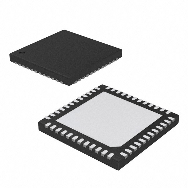
Small 48-pin LQFP and VQFN Packages
Full-Duplex Vocoding (CMX638 only)
1.
DMR TDMA
VoIP Systems
Voice Pagers
Brief Description
The CMX608/CMX618/CMX638 are flexible, high integration, high performance, RALCWI (Robust
Advanced Low Complexity Waveform Interpolation) Vocoders, offering near toll quality voice at very low bit
rates. A Forward Error Correction (FEC) engine provides optimum performance in real life applications.
The RALCWI Vocoder comprises four independent functions which are selectable by the host: Voice
Encoder, FEC Encoder, Voice Decoder and FEC Decoder. The CMX608 and CMX618 are half-duplex
Vocoders and the CMX638 is a full-duplex Vocoder with integrated voice CODEC.The CMX618 includes
an integrated voice CODEC, offering a complete analogue voice to low bit rate vocoded data function, with
integrated channel filters removing the need for external components, whereas the CMX608 requires an
external voice CODEC.
CMX608/CMX618/CMX638 operate from a dual power supply (1.8V and 3.3V) and are available in both
48-pin LQFP (L4) and 48-pin VQFN (Q3) packages.
2014 CML Microsystems Plc
Continued overleaf .....
�RALCWI Vocoder
CMX608/CMX618/CMX638
In encode mode, the voice encoder uses a 20ms voice frame size with two programmable bit rates:
2400bps or 2750bps. The optional FEC encoder performs channel coding of the encoded voice (2400bps
or 2750bps, depending on the selected mode) and forms an encoded, interleaved bit-stream of 3600bps
(216 bits per 60ms packet or 288 bits per 80ms packet). The FEC operation utilises a packet of either 3 or
4 x 20ms Vocoder frames to provide optimum error correction performance.
In decode mode, the optional FEC decoder performs de-interleaving and channel decoding of the coded
bit-stream (216 bits per 60ms packet or 288 bits per 80ms packet) and forms an error-corrected bit-stream
of encoded voice at 2400bps or 2750bps rate, depending on the selected mode. The FEC decoder can
optionally use "soft decision" metrics to improve its decoding ability. The voice decoder then converts the
error-corrected bit-stream back into a digitised voice signal.
Soft Decision Decoding (SDD), Discontinuous Transmission detection (DTX), Voice Activity Detection
(VAD) and Comfort Noise Generation (CNG) functions are also included, to further enhance the overall
performance. Single (STD) and Dual (DTMF) Tones can be detected and sent separately in the coded bitstream, then regenerated at the far end.
New features and enhancements to existing functions may be provided from time to time, expanding the
capabilities of the Vocoder. These are provided as Function Images™, a hex format file that can be loaded
via the C-BUS at run-time. Function Images™ can be downloaded from the CML Portal, a secure area of
the CML website. Details of currently available Function Images™ can be found in the
CMX608/CMX618/CMX638 Product page on the CML website.
2014 CML Microsystems Plc
2
D/608_18_38/11
�RALCWI Vocoder
CMX608/CMX618/CMX638
CONTENTS
Section
Page
1.
Brief Description ..................................................................................................................... 1
2.
Block Diagram ......................................................................................................................... 5
3.
Signal List ................................................................................................................................ 6
4.
External Components ............................................................................................................. 9
4.1. PCB Layout Guidelines and Power Supply Decoupling ................................................. 11
4.2. Audio CODEC External Components (CMX618/CMX638 only) .................................... 12
5.
General Description .............................................................................................................. 13
5.1. Initialisation .................................................................................................................... 14
5.2. Encoder .......................................................................................................................... 15
5.2.1. Single Frame Packet, without FEC, STD or DTMF .............................................. 15
5.2.2. Multiple Frame Packet with FEC, but without STD or DTMF ............................... 16
5.3. Decoder ......................................................................................................................... 16
5.3.1. Single Frame Packet, without FEC, STD or DTMF .............................................. 17
5.3.2. Multiple Frame Packet with FEC, but without STD or DTMF ............................... 19
5.4. Overall Signal Latency ................................................................................................... 20
5.5. Vocoder Data Format and Bit Order .............................................................................. 20
5.5.1. Packets of Raw Vocoder Frames ........................................................................ 20
5.5.2. Packets of FEC Protected Frames ...................................................................... 22
5.6. External CODEC Support .............................................................................................. 23
5.7. Operation with DTMF (Dual Tone Multi-Frequency) ...................................................... 26
5.7.1. DTMF Transmit .................................................................................................... 26
5.7.2. DTMF Receive ..................................................................................................... 26
5.7.3. DTMF Format ....................................................................................................... 27
5.8. Operation with STD (Single Tones) ............................................................................... 28
5.9. C-BUS Interface ............................................................................................................. 29
5.10. C-BUS Registers............................................................................................................ 32
5.10.1. Command Registers ............................................................................................ 32
5.10.2. 8 Bit Write-Only Registers .................................................................................... 33
5.10.3. 8 Bit Read-Only Registers .................................................................................... 44
5.10.4. 16-bit Write-Only Registers .................................................................................. 46
5.10.5. 16-bit Read-Only Registers .................................................................................. 51
6.
Application Notes.................................................................................................................. 55
6.1. Basic Operation of the Vocoder ..................................................................................... 55
6.2. FEC and LLR Decoding ................................................................................................. 57
6.3. DTX and SID Functions ................................................................................................. 57
6.4. Single Tone Transfer ..................................................................................................... 57
6.5. Slip Management ........................................................................................................... 57
6.6. Setting the Watermarks for the Vocoder Data Input (Output) FIFOs ............................ 59
6.7. Download Protocol for Function Images™ .................................................................... 59
6.8. Using the PLEVEL register to set the Input Gain ........................................................... 60
7.
Performance Specification ................................................................................................... 61
7.1. Electrical Performance ................................................................................................... 61
7.1.1. Absolute Maximum Ratings ................................................................................. 61
7.1.2. Operating Limits ................................................................................................... 61
7.1.3. Operating Characteristics ..................................................................................... 62
7.2. Packaging ...................................................................................................................... 68
2014 CML Microsystems Plc
3
D/608_18_38/11
�RALCWI Vocoder
CMX608/CMX618/CMX638
Table
Table 1
Table 2
Table 3
Table 4
Table 5
Table 6
Table 7
Page
Clock/Crystal Selection .....................................................................................................10
DTMF - Format 1...............................................................................................................27
Standard DTMF Keypad Layout ........................................................................................28
DTMF - Format 2...............................................................................................................28
C-BUS Register Addresses ...............................................................................................31
Decoder Packet Description ..............................................................................................43
Encoder Packet Description ..............................................................................................45
Figure
Page
Figure 1 Block Diagram ....................................................................................................................5
Figure 2 CMX608 Recommended External Components ................................................................9
Figure 3 CMX618/CMX638 Recommended External Components ...............................................10
Figure 4 CMX618/CMX638 Power Supply and De-coupling ..........................................................11
Figure 5 Recommended External Components – Differential CODEC Inputs ...............................12
Figure 6 Recommended External Components – Single-ended CODEC Inputs ...........................12
Figure 7 Recommended External Components – CODEC Output ................................................12
Figure 8 Single Frame Packet Encoding ........................................................................................15
Figure 9 Multiple Frame Packet Encoding .....................................................................................16
Figure 10 Single Frame Packet Decoding .....................................................................................18
Figure 11 Single Frame Packet Decoding with Host Jitter .............................................................18
Figure 12 Single Frame Packet Decoding with Host Jitter (Increased IDD) ..................................19
Figure 13 Multiple Frame Packet Decoding ...................................................................................19
Figure 14 Overall Signal Latency ...................................................................................................20
Figure 15 PCM3500 Interface ........................................................................................................25
Figure 16 Basic C-BUS Transactions ............................................................................................29
Figure 17 C-BUS Data-Streaming Operation .................................................................................30
Figure 18 C-BUS Timing ................................................................................................................66
Figure 19 CODEC (SSP) Port Timing (Slave Mode) ......................................................................66
Figure 20 ADC Input Filter - Typical Response ..............................................................................67
Figure 21 DAC Output Filter - Typical Response ...........................................................................67
Figure 22 48-pin LQFP Mechanical Outline (L4) ...........................................................................68
Figure 23 48-pin VQFN Mechanical Outline (Q3) ..........................................................................69
It is always recommended that you check for the latest product datasheet version from the Datasheets
page of the CML website: [http://www.cmlmicro.com/].
History
Version
11
10
9
8
7
6
Changes
Editorial improvements
Corrected the lack of termination of the SYNC pin (pin 25)
Corrected minor rerrors and the table definition of bits 2, 3 in section 5.10.1.
Clarified the function of the ENABXTAL and RESETN/General Reset functions.
Added power supply ground plane layout drawing.
Clarification of when to write packets in full duplex mode
Information added about loading Function Images™ into the device
Clarification on choice of Xtal and Clock speed
Clarification on use of the CLOCK and DTMFATTEN registers
Information added about use of the PLEVEL (peak level) register
Corrections to "Basic Operation of the Vocoder" (section 6.1) and to "Download
Protocol for Function Updates" (section 6.7)
Typical IDD Digital current consumption figure amended for full duplex mode
Correction to the description of dPMR frames in section 5.4.2
First Release of document with CMX638 (full-duplex device) included
2014 CML Microsystems Plc
4
Date
19.09.14
31.07.12
19.05.09
12.12.08
18.07.08
19.03.08
D/608_18_38/11
�RALCWI Vocoder
2.
CMX608/CMX618/CMX638
Block Diagram
Figure 1 Block Diagram
2014 CML Microsystems Plc
5
D/608_18_38/11
�RALCWI Vocoder
3.
CMX608/CMX618/CMX638
Signal List
CMX608/
CMX618/
CMX638
L4/Q3
Signal
Description
Pin No.
Name
Type
1
AVDD
Power
2
AVSS
Power
3
BIAS
Analogue
Output
4
VSSREF
Power
5
INPUT P
Analogue
Input
6
INPUT N
Analogue
Input
7
AVDD
Power
8
AVSS
Power
9
VSSPA
Power
10
OUT P
Analogue
Output
11
OUT N
Analogue
Output
12
VDDPA
Power
13
VDD
Power
Digital Positive Power Supply 1.8V
14
IOVDD
Power
Digital I/O Positive Power Supply 3.3V
15
SDI
Digital Input
16
SDO
Digital
Output
SSP port serial data output
17
SCLK
Digital Input
SSP port serial clock input
18
STRB
Digital Input
SSP port serial strobe input
2014 CML Microsystems Plc
CMX618/CMX638: Analogue Positive Power Supply 3.3V
CMX608: Not used (connect to IOVDD)
CMX618/CMX638: Analogue Negative Power Supply 0V
CMX608: Not used (connect to VSS)
CMX618/CMX638: Analogue Bias (approximately 1.65 Volts)
CMX608: Not used (leave unconnected)
CMX618/CMX638: Analogue Negative Reference
CMX608: Not used (connect to VSS)
CMX618/CMX638: Audio CODEC Positive Input (self biased)
CMX608: Not used (leave unconnected)
CMX618/CMX638: Audio CODEC Negative Input (self biased)
CMX608: Not used (leave unconnected)
CMX618/CMX638: Analogue Positive Power Supply 3.3V
CMX608: Not used (connect to IOVDD)
CMX618/CMX638: Analogue Negative Power Supply 0V
CMX608: Not used (connect to VSS)
CMX618/CMX638: Output Amplifier Negative Power Supply 0V
CMX608: Not used (connect to VSS)
CMX618/CMX638: Audio CODEC – Amplifier Positive Output
CMX608: Not used (leave unconnected)
CMX618/CMX638: Audio CODEC – Amplifier Negative Output
CMX608: Not used (leave unconnected)
CMX618/CMX638: Output Amplifier Positive Power Supply 3.3V
CMX608: Not used (connect to IOVDD)
SSP port serial data input
6
CODEC PORT
D/608_18_38/11
�RALCWI Vocoder
CMX608/CMX618/CMX638
CMX608/
CMX618/
CMX638
L4/Q3
Signal
Description
Pin No.
Name
Type
19
EEC
Digital
Output
Enable external CODEC, controlled by the C-BUS
20
REC
Digital
Output
Reset external CODEC, controlled by the C-BUS
21
NC
22
VSS
Reserved for future use. Do not connect to this pin.
Power
CMX608: Reserved for future use. Do not connect to this pin.
NC
23
Negative Power Supply 0V
CMX618/CMX638: CODEC Select (Internal if '1', External if '0')
CSEL
Digital Input
24
IOVDD
Power
25
SYNC
Digital
Input/Output
26
VSS
Power
27
XTALin
Input
28
XTALout
Output
Crystal Output
29
IOVDD
Power
Digital I/O Positive Power Supply 3.3V
30
RESETN
Digital Input
31
XTALSEL1
Digital Input
32
XTALSEL2
Digital Input
33
XTALSEL3
Digital Input
34
ENABXTAL
Digital Input
35
IOVDD
Power
36
NC
Reserved for future use. Do not connect to this pin.
37
NC
Reserved for future use. Do not connect to this pin.
38
NC
Reserved for future use. Do not connect to this pin.
39
NC
Reserved for future use. Do not connect to this pin.
40
NC
Reserved for future use. Do not connect to this pin.
41
VSS
Power
42
CLK
Digital Input
C-BUS Serial Clock
43
CDATA
Digital Input
C-BUS Command Data
44
RDATA
Tri-state
Output
45
CSN
Digital Input
C-BUS Chip Select (bar)
46
IRQN
Open Drain
Digital
Output
C-BUS Interrupt Request (bar)
2014 CML Microsystems Plc
This pin must be connected to either IOVDD or VSS.
Digital I/O Positive Power Supply 3.3V
Synchronisation Input/Output. By default, this pin is an input
and must be connected by the user to either IOVDD or VSS.
Negative Power Supply 0V
Crystal Input
General Reset (active low)
These bits select the crystal/clock frequency,
according to Table 1.
Enable Crystal Oscillator/External Clock Input
Digital I/O Positive Power Supply 3.3V
Negative Power Supply 0V
C-BUS Reply Data
C-BUS
7
D/608_18_38/11
�RALCWI Vocoder
CMX608/CMX618/CMX638
CMX608/
CMX618/
CMX638
L4/Q3
Signal
Description
Pin No.
Name
Type
47
IOVDD
Power
Digital I/O Positive Power Supply 3.3V
48
VDD
Power
Digital Positive Power Supply 1.8V
EXPOSED
METAL
PAD
SUB
NC
2014 CML Microsystems Plc
On the Q3 package only, the central metal pad may be connected to
Analogue Ground (Avss) or left unconnected.
No other electrical connection is permitted.
8
D/608_18_38/11
�RALCWI Vocoder
4.
CMX608/CMX618/CMX638
External Components
CBUS
IOVDD
C9
VDD
Vss
NC
IOVDD
IOVDD
C4
Vss
39
38
NC
NC
40
NC
Vss
41
NC
Vss
42
NC
NC
43
Vss
Vss
44
CLK
Vss
45
CDATA
Vss
46
RDATA
C7
47
CSN
48
IOVDD
IRQN
VDD
Vss
IOVDD
Vss
R2
IOVDD
C5
37
1
36
2
35
NC
IOVDD
IOVDD
C8
Vss
ENABXTAL
3
34
4
33
5
32
XTALSEL3
XTALSEL2
CMX608
6
7
31
IOVDD
XTALSEL1
D1
30
IOVDD
8
29
9
28
10
27
Vss
IOVDD
Vss
Vss
NC
NC
IOVDD
IOVDD
C10
11
26
12
25
Vss
XTAL out
XTAL
XTAL in
C1
13
15
16
17
18
19
20
21
22
23
Vss
C11
Vss
IOVDD
C6
Vss
Vss
Vss
CODEC PORT
C1
C2
C3
C4
C5
C6
C7
C8
Vss
24
IOVDD
NC
Vss
NC
REC
EEC
STRB
SCLK
SDO
SDI
IOVDD
VDD
Vss
14
C2
Vss
SYNC
VDD
C3
C12
Vss
Vss
R1
RESETN
22pF
22pF
1.0µF
100nF
1.0µF
100nF
100nF
100nF
C9
C10
C11
C12
100nF
100nF
1.0µF
100nF
R1
R2
D1
470k
100k
small signal diode
Notes: 1. On CMX608/CMX618/CMX638 devices, the crystal selection pins (XTALSEL1, XTALSEL2
and XTALSEL3) must be permanently tied to either IOVDD or VSS and not driven from a logic
level output of the host µController (see Table 1 for a list of crystal frequencies). For 9.6MHz
and 12.0MHz operation, either a crystal or a clock can be used. For all other frequencies, a
clock must be injected into the XTALIN pin and the XTALOUT pin must be left unconnected.
2. To use the CMX608/CMX618/CMX638, tie the ENABXTAL pin to IOVDD. If the ENABXTAL pin
is connected to VSS it will force the device into a deep powersave mode, where the C-BUS
interface and clock input (XTALIN) are disabled and the crystal oscillator is powered down.
3. A single 10µF electrolytic capacitor may be fitted in place of C5 and C11, providing the two
VDD pins are connected together on the pcb with an adequate width power supply trace.
Figure 2 CMX608 Recommended External Components
2014 CML Microsystems Plc
9
D/608_18_38/11
�RALCWI Vocoder
CMX608/CMX618/CMX638
CBUS
IOVDD
C9
VDD
Vss
39
38
NC
40
NC
41
NC
42
NC
43
Vss
44
CLK
45
CDATA
AVss
46
RDATA
C7
47
CSN
48
AVDD
IRQN
VDD
Vss
AVDD
Vss
R2
IOVDD
C5
37
1
36
2
35
NC
IOVDD
IOVDD
C8
AVss
AVss
C14
BIAS
VssREF
AVss
AVss
INPUT P
3
34
4
33
CMX618/
CMX638
5
INPUT N
AVDD
6
AVDD
C4
AVss
7
8
AVss
AVss
VssPA
AVss
OUT P
OUT N
VDDPA
VDDPA
C10
XTALSEL3
XTALSEL2
32
31
IOVDD
29
28
10
27
11
26
12
25
13
14
15
16
17
18
19
20
21
22
23
C3
Vss
IOVDD
C12
Vss
XTAL out
XTAL
XTAL in
C1
C2
Vss
SYNC
VDD
R1
RESETN
Vss
Vss
Vss
24
IOVDD
CSEL
Vss
NC
REC
EEC
STRB
SCLK
SDO
SDI
IOVDD
VDD
IOVDD
C11
C6
Vss
Vss
Vss
CODEC PORT
Vss
C1
C2
C3
C4
C5
C6
IOVDD
XTALSEL1
D1
30
9
AVss
IOVDD
C13
Vss
ENABXTAL
22pF
22pF
1.0µF
100nF
1.0µF
100nF
C7
C8
C9
C10
C11
C12
100nF
100nF
100nF
100nF
1.0µF
100nF
C13
C14
100nF
100nF
R1
R2
D1
470k
100k
small signal diode
Figure 3 CMX618/CMX638 Recommended External Components
Crystal Select Input Pins:
XTALSEL3 XTALSEL2
0
0
0
1
1
1
1
0
1
1
0
0
1
1
XTALSEL1
Clock/Crystal
Frequency
Clock/Crystal Choice
1
0
1
0
1
0
1
9.6MHz
12.0MHz
14.4MHz
16.8MHz
19.2MHz
21.6MHz
24.0MHz
crystal or clock
crystal or clock
external clock only
external clock only
external clock only
external clock only
external clock only
Table 1 Clock/Crystal Selection
2014 CML Microsystems Plc
10
D/608_18_38/11
�RALCWI Vocoder
4.1.
CMX608/CMX618/CMX638
PCB Layout Guidelines and Power Supply Decoupling
Figure 4 CMX618/CMX638 Power Supply and De-coupling
Component Values as per Figure 3.
Notes:
It is important to protect the analogue pins from extraneous inband noise and to minimise the impedance
between the CMX618/CMX638 and the power supply and bias de-coupling capacitors. The de-coupling
capacitors C4, C6, C7, C8, C9, C10, C12, C13 and C14 should be as close as possible to the
CMX618/CMX638. It is therefore recommended that the printed circuit board is laid out with separate
ground planes for the AVSS and (digital) VSS supplies in the area of the CMX618/CMX638, with provision
to make links between them close to the CMX618/CMX638. The use of a multi-layer printed circuit board
will facilitate the provision of ground planes on separate layers. The layout of a CMX608 printed circuit
board should make use of a single ground plane covering the whole chip area shown above.
On CMX618/CMX638, VBIAS is used as an internal reference for detecting and generating the various
analogue signals. It must be carefully decoupled, to ensure its integrity, so apart from the decoupling
capacitor shown, no other loads should be connected. If VBIAS needs to be used to set an external midpoint reference, it must be buffered with a high input impedance buffer.
2014 CML Microsystems Plc
11
D/608_18_38/11
�RALCWI Vocoder
4.2.
CMX608/CMX618/CMX638
Audio CODEC External Components (CMX618/CMX638 only)
Figure 5 Recommended External Components – Differential CODEC Inputs
Figure 6 Recommended External Components – Single-ended CODEC Inputs
Note: Care should be taken to avoid shorting OUTP and OUTN together, or shorting either OUTP or OUTN to Vss or Vdd.
An external RC filter could be added across the OUTP and OUTN pins if clock noise needs further reduction.
C9
C10
C11
C12
R3
R4
470nF
470nF
1.0µF
100µF
1.0kΩ
1.0kΩ
Figure 7 Recommended External Components – CODEC Output
2014 CML Microsystems Plc
12
D/608_18_38/11
�RALCWI Vocoder
5.
CMX608/CMX618/CMX638
General Description
The CMX608/CMX618/CMX638 are a pin-compatible family of near toll quality voice encoders/decoders
(Vocoders). The voice encoding/decoding is performed by a new, low data rate algorithm which is based
on Robust Advanced Low Complexity Waveform Interpolation (RALCWI) technology. The data rate is
selectable between 2400bps or 2750bps (all without FEC) or 3600bps (with FEC). The frame length is
selectable from 20ms, 40ms, 60ms or 80ms (all without FEC) or from 60ms or 80ms (with FEC). The
integral Viterbi FEC decoder can optionally use "soft decision" metrics to improve its decoding ability if the
signal can be applied in a 4-bit digital representation of the received/demodulated analogue signal. The
FEC can also be used on its own, so that data can be decoded/error-corrected then re-encoded and
forwarded on. This allows use in a digital voice repeater.
RALCWI technology uses unique proprietary signal decomposition and parameter encoding methods,
ensuring high voice quality at high compression ratios. The voice quality of RALCWI-class Vocoders, as
estimated by independent listeners, is similar to that provided by standard Vocoders running at bit rates
above 4000 bps. The Mean Opinion Score (MOS) of voice quality for this Vocoder is about 3.5-3.6. This
value was determined by a paired comparison method, performing listening tests of developed and
standard voice Vocoders.
The RALCWI Vocoder operates on a “frame-by-frame” basis. The 20ms source voice frame consists of
160 samples of linear 16-bit PCM sampled at 8kHz. The Voice Encoder performs voice analysis at the
high time resolution (8 times per frame) and forms a set of estimated parameters for each voice segment.
All of the estimated parameters are quantized to produce 48- or 55-bit frames, using Vector Quantization
(VQ) of different types. All of the vector quantizers were trained on a mixed multi-language voice base,
which contains voice samples in both Eastern and Western languages.
Voice parameters are coded by the Voice Encoder with high efficiency. Sensitivity to errors is estimated
for each output bit and a bit frame is split into two parts: “more sensitive to errors” and “less sensitive to
errors”. To protect the voice parameters against channel errors without reducing voice quality, the “more
sensitive” bits are protected. Such protection is provided by the FEC Encoder/Decoder mechanism. The
Voice Decoder de-quantizes the parameters and re-synthesizes the voice.
Control of the CMX608/CMX618/CMX638 is over a C-BUS serial port from the host µC. On the
CMX618/CMX638 only, the CSEL pin allows the selection of an internal or external CODEC, by connecting
the CSEL pin to either IOVDD or VSS respectively. If the internal CODEC is selected, the SDI, STRB and
SCLK pins should be connected to Vss. Synchronisation to the host µC is by use of either the (rising-edge
active) SYNC input or by writing to the SYNC register ($02). All major data paths are buffered in each
direction with FIFO registers. The SSP port, which is used for the external ADC serial input and DAC serial
output, is buffered in this way, as is the data to and from the CODEC (CMX618/CMX638 only) and also the
vocoded data which is streamed into and out of the C-BUS interface. The management of these FIFOs is
handled automatically and does not require any user intervention, other than the supply or consumption of
data at the appropriate rate.
On the CMX618/CMX638 only, a voice CODEC is included, consisting of a microphone input to an ADC
and a DAC with an earpiece output. A variable gain stage is associated with each converter. The
differential input stage includes 20dB of switchable gain, for use as a microphone pre-amplifier. The input
gain blocks are provided to allow for inputs from different microphone or other audio devices. At the very
highest gain combinations, the input noise may start to be significant. In this case, users may wish to
consider an external low-noise preamplifier prior to the differential input stage. For most applications this
will not be necessary. The differential output stage includes 6dB of switchable gain. By using the output
stage in a differential configuration, a further 6dB of gain can be achieved. Both input and output stages
include a high-order digital channel filter, to constrain the input and output signals to an audio bandwidth of
4kHz. See Figure 20 and Figure 21 for further details. This avoids the necessity of adding external third
(or higher) order filters, thus saving external components. A small number of external components, as
shown in Figure 5, Figure 6 and Figure 7 is all that is required to implement the analogue interfaces to the
CMX618/CMX638 voice CODEC.
2014 CML Microsystems Plc
13
D/608_18_38/11
�RALCWI Vocoder
CMX608/CMX618/CMX638
The CMX608 (and the CMX618/CMX638, if the internal CODEC is not selected) provides a synchronous
serial port (SSP), enabling a wide range of external CODECs to be used with this device. Two digital
outputs, EEC and REC, can be used to enable and reset the external CODEC. They are controlled by bit 0
(EEC) and bit 1 (REC) of the EXCODECCONT register ($0B). On the CMX618/CMX638 only, when the
internal CODEC is selected, these pins are available as uncommitted digital outputs instead.
In CMX608/CMX618/CMX638, DTMF and single tones (STD) can be sent and received reliably over a
noisy channel by using the special control codes, see section 5.7. Both devices feature a DTX
(Discontinuous Transmission) mode, where an integral Voice Activity Detector in the encoder will send SID
(Silence Insertion Description) data to the decoder, which will perform Comfort Noise Generation.
The CMX608 and CMX618 devices can operate in a mode that reduces the current consumption when the
device is not actively being used, at the expense of a small reduction in maximum C-BUS SCLK frequency
and an increase in the difference between the peaks and troughs of current consumption when running.
This mode is known as 'clock-throttling', where the vocoder's internal clock rate is automatically set to a
quarter of its normal value when the device is waiting for samples or packets, i.e. not actively engaged in
encoding or decoding. Clock throttling is not available on the CMX638.
This mode is enabled by setting bit 4 of the POWERSAVE register ($09) to '1' after the device has been
reset. The typical overall current consumption with "clock throttling" enabled can be calculated from the
following figures:
(3.3V) IDD Total = IDD IODigital + IDD Analogue + IDD Analogue PA = 7.8 mA when encoding
(3.3V) IDD Total = IDD IODigital + IDD Analogue + IDD Analogue PA = 4.1 mA when decoding.
(1.8V) IDD Total = IDD Digital = 33.0 mA when encoding and = 20.0 mA when decoding
For the CMX638, clock throttling is not possible, so the typical Full-duplex current consumption figures are:
(3.3V) IDD Total = IDD IODigital + IDD Analogue + IDD Analogue PA = 11.3 mA
(1.8V) IDD Total = IDD Digital = 49.0 mA
5.1.
Initialisation
On first applying power, three actions have to be performed: the crystal oscillator has to start up (if used),
the bias chain has to be powered up (CMX618/CMX638 only), so that the decoupling capacitor (C14) has
charged to AVDD / 2, and on-chip digital circuits have to be reset into a known state. The crystal oscillator
typically takes much less than 20ms to start up, but the actual time will depend on the ESR of the crystal
used. With the components shown in Figure 3, the BIAS pin will take 100ms typically to reach its steadystate value of AVDD / 2. There are two sources of reset:
o pulling the RESETN signal (pin 30) to '0' for at least 200ns, then returning it to '1' (the pin does not
have an internal pullup resistor). Note that the device does not have an automatic power-up reset.
o writing to the C-BUS RESET register ($01). This is a 1-byte command which has no data.
A hard reset (taking RESETN low) will also force the ENABXTAL signal low, which disables the clock and
powersaves the crystal oscillator. On first applying power, the RESETN pin should be held low until all the
power supplies have stabilised, to ensure correct operation of the device. When coming out of a hard
reset, the device needs the crystal oscillator to be working, then counts 65,536 clock cycles (= 5.4ms delay
with a 12.0MHz clock), then automatically performs a soft reset by writing to the C-BUS RESET register.
A soft reset (writing to the RESET register) will clear all registers to '0', unless noted otherwise – in which
case the default settings are restored. The device will be ready to accept C-BUS commands approximately
1.5ms after completion of the soft reset action and will indicate that it is ready by setting bit 15 of the
STATUS register ($40) to '1' and also by indicating a C-BUS interrupt request by pulling the IRQN pin low.
Note that on reset, the IRQENAB register ($1F) bit 15 will automatically be set to '1', thus enabling the
RDY interrupt to activate the IRQN pin. Refer also to section 6.1 for a description of the start-up sequence.
Connecting the ENABXTAL pin to VSS when the device is operational will force the device into a powersave mode where the C-BUS interface and clock input (XTALIN) are disabled and the crystal oscillator is
powered down. However, the BIAS pin and C-BUS registers are not disturbed, so normal operation can be
resumed by re-connecting the ENABXTAL pin to IOVDD and waiting for the crystal oscillator to re-start.
2014 CML Microsystems Plc
14
D/608_18_38/11
�RALCWI Vocoder
CMX608/CMX618/CMX638
5.2.
Encoder
The encoder deals with a basic frame size of 20ms, 160 samples, of audio. 1, 2, 3, or 4 frames may be
collected together and supplied to the host as a single packet. In the case of the 3 and 4 frame packets,
error protection may also be added with the FEC option. The encoder can also detect single tones (STD)
and/or DTMF in the audio stream. If detected, special frames are produced which the decoder will
recognise and deal with accordingly.
The exact rate at which packets are produced is dependant on the accuracy of the CODEC's sample rate.
The nominal rate is every 20ms, or a multiple thereof, depending on the number of frames that make up
the packet. For instance, a packet of 3 frames with FEC will be produced every 60ms. The algorithm used
to encode voice has algorithmic jitter, i.e. it does not take the same amount of time to encode each frame.
Some frames will take longer than others, consequently, the exact time that a packet will be available is
not predictable. The encoder will notify the host as soon as a packet becomes available. Over a period of
time the average rate will be every 20ms (or a multiple thereof) according to the CODEC's sample rate.
Once a packet of data becomes available, the host may read it straight away, or it can wait for a period of
time. The packet will remain available until the next one is produced.
5.2.1.
Single Frame Packet, without FEC, STD or DTMF
This is the simplest and most basic configuration. The encoder will produce a one-frame raw Vocoder
packet every 20ms. Once the encode instruction is given, the device will collect 20ms (160 samples) worth
of audio. These 160 samples will be given to the encoder to process. The processing of these samples will
take no more than 15ms, therefore the first packet of data will be available no later than 35ms after the
device was instructed to encode.
There are two basic strategies that can be adopted for servicing the encoder:
Event-driven
The host may use the C-BUS interrupt, IRQN, or poll the STATUS register, then read the Vocoder packet
as soon as it becomes available. This is signified by bit 0 (VDA) of the STATUS register being set to '1'.
The host may then choose to hold the packet in a buffer until the correct time to process it arrives. In the
case of a voice recorder, the packet could be put into a storage device immediately. In the case of some
sort of transmission (radio or network), the packet may be held until the correct time-slot arrives.
Timed
Assuming the host has an accurate 20ms timer derived from the same master clock as that supplied to the
audio CODEC (this could be the Vocoder device, or an external CODEC), wait for a timer event and then
instruct the device to encode. Wait for two more timer events, then read the first Vocoder packet. For
every subsequent timer event, read another Vocoder packet. Figure 8 shows the sequence of events.
Figure 8 Single Frame Packet Encoding
2014 CML Microsystems Plc
15
D/608_18_38/11
�RALCWI Vocoder
CMX608/CMX618/CMX638
This timed method may also be used where the host clock and CODEC clock are unrelated, in which case
the host must supply a synchronising signal. Further details of slip management are given in section 6.5.
5.2.2.
Multiple Frame Packet with FEC, but without STD or DTMF
This is the most suitable configuration for use in a wireless system where the channel is prone to bit errors.
Two modes are available:
3 frame packet, which represents 60ms of voice. This mode is most suitable for TDMA/DMR.
4 frame packet, which represents 80ms of voice. This mode is most suitable for FDMA/DMR.
Figure 9 shows the 3 frame mode, but the principal applies equally to the 4 frame mode. There are two
basic strategies that can be adopted for servicing the encoder:
Event-driven
This is exactly the same as for the single frame example. Bit 0 (VDA) in the STATUS ($40) register will be
set to '1' when an FEC protected frame becomes available. If interrupts are enabled then IRQN will also
be pulled low.
Timed
It is assumed that the host has an accurate method of timing, as discussed in the single frame example.
Instruct the device to encode. Wait for 80ms, then read the first Vocoder packet. Wait for 60ms before
reading the next and subsequent packets.
Figure 9 Multiple Frame Packet Encoding
Figure 9 shows the sequence of events. Adding the FEC is shown twice, though it is only executed once.
rd
This is to show that it will start immediately after the 3 vocoded frame is available - which depends on the
algorithmic jitter for that frame.
In the case of 4 frame packets, the initial wait should be 100ms and the subsequent waits should be 80ms.
5.3.
Decoder
Like the encoder, the decoder deals with a basic frame size of 20ms, 160 samples, of audio. 1, 2, 3, or 4
frames may be collected together and supplied to the decoder as a single packet. In the case of the 3 and
4 frame packets, error protection may also be included with the FEC option. FEC protected packets may
contain either soft bits or hard bits. A soft-bit packet is 4 times the size of a hard-bit packet, as each softbit is represented by a nibble. The decoder can also detect special STD and DTMF frames and reproduce these as tones in the audio stream.
2014 CML Microsystems Plc
16
D/608_18_38/11
�RALCWI Vocoder
CMX608/CMX618/CMX638
The exact rate at which packets must be presented is dependant on the accuracy of the CODEC's sample
rate. The nominal rate is every 20ms, or a multiple thereof, depending on the number of frames that make
up the packet. For instance, a packet of 3 frames with FEC will be produced every 60ms. The algorithm
used to decode the encoded voice has algorithmic jitter, i.e. it does not take the same amount of time to
decode each frame. Some frames will take longer than others. An initial delay in sending samples to the
CODEC, coupled with an output buffer, will ensure that the CODEC is not starved of samples. It is also
possible for the decoder to indicate that a new packet should be presented for decoding, based upon the
number of samples left in the output buffer.
5.3.1.
Single Frame Packet, without FEC, STD or DTMF
This is the simplest and most basic configuration. The decoder will produce 20ms of audio for each
single-frame raw Vocoder packet.
Once the decode instruction is given, the device will wait for single-frame raw Vocoder packets to arrive
every 20ms. Once the first packet is received, the initial decoder delay timer will be started, the frame will
be decoded into 20ms of audio samples and the resulting samples placed in the output buffer. After the
samples have been placed in this buffer, the device will wait for the initial decoder delay (IDD) timer to
expire before sending the first sample to the CODEC. After this initial delay, further samples are given to
the CODEC at its sample rate. The initial delay is set to be greater than the maximum time it takes to
decode a frame. This ensures that the CODEC will not be starved of samples if the subsequent frame
takes longer to decode than the first frame. The default initial decoder delay is set to 64 samples (8ms),
which is more than sufficient to cover the internal algorithmic jitter. If the host, either through its internal
scheduling or as a result of any algorithmic jitter in any processing that has to occur (e.g. demodulation),
cannot supply the packets at exactly the right time (even though the average interval is correct), this initial
delay should be increased to cover the additional jitter. The IDD ($0C) register has been provided in order
to facilitate the adjustment of this delay.
The CMX608 and CMX618 can be configured to set the STATUS ($40) register bit 8 (VDW Vocoder Data
Wanted) to '1' whenever there are fewer than a certain number of samples left in the output buffer. This is
controlled by the low and high watermarks, which are set by using the VDWHLWM ($1E) register. When
the number of samples left in the output buffer is less than or equal to the low watermark, VDW will be set
to '1' (and a C-BUS interrupt will occur, if enabled). Once indicated, the VDW bit cannot be set again until
the output buffer has had at least 'high watermark' samples in it. This hysteresis prevents constant
indication or interrupts when the number of samples in the buffer is still less than the low watermark.
There are three basic strategies that can be adopted for driving the decoder:
Event driven / Method 1
The host may use the C-BUS interrupt, IRQN, or poll the STATUS register, then supply a Vocoder packet
as soon as the VDW bit is set. For this method the low and high watermarks must be set to suitable
values. As an example, given that the decoder algorithm will take no more than 8ms to process a frame,
and that the host can respond to the STATUS register having its VDW bit set within 1 ms, the low
watermark should be set for a time period of 9ms, where 9ms at 8000 samples per second equates to a
period of 72 samples. The high watermark should be set to a few samples less than 160. This value is
not critical, providing it is greater than the low watermark.
The host should send the first packet to the device, after which it should wait, either by polling or by
making use of the C-BUS interrupt, for the VDW bit to be set to '1'. Once this bit is set, the next packet
should be sent to the device. The process should be repeated for as long as there are packets to decode.
This method is an ideal choice for a voice record/playback system.
Event driven / Method 2
The device can be set up to produce a short pulse every 20ms on the SYNC pin (pin 25). This pulse can
be used to signal an interrupt to the controlling host, which can then cause a packet of data to be sent to
the Vocoder. The 20ms period is directly related to the sample rate of the internal CODEC. This will only
work for a CMX618/CMX638 set up for using its internal CODEC. For the CMX608, or the
2014 CML Microsystems Plc
17
D/608_18_38/11
�RALCWI Vocoder
CMX608/CMX618/CMX638
CMX618/CMX638 in external CODEC mode, the SYNC output is not available, so another method needs
to be employed, e.g using a modulo 160 counter clocked by the CODEC frame sync.
Timed
It is assumed that the host has an accurate 20ms timer, derived from the master clock of the system,
which may or may not be synchronous with the audio CODEC. Wait for a timer event, instruct the device
to decode, and then supply a packet for decoding. For every subsequent timer event, supply another
packet for decoding. This is essentially the same as the event driven / method 2 above, the difference
being that if the timer is not synchronous with the CODEC then the device's slip management feature will
have to be employed. Further details of slip management are given in section 6.5.
The following diagrams show various aspects of the timed delivery of single-frame raw Vocoder packets
for decoding.
Figure 10 Single Frame Packet Decoding
Figure 10 shows the sequence of events including the initial decoder delay, which compensates for the
decoder's algorithmic jitter.
Figure 11 Single Frame Packet Decoding with Host Jitter
Figure 11 shows the effect of 4ms of host jitter with a default value of 8ms for the initial decoder delay.
After the second batch of samples there is a gap, where the worst case of early delivery followed by late
delivery has caused the CODEC to be starved of samples. To avoid this situation, the IDD has to be
increased.
2014 CML Microsystems Plc
18
D/608_18_38/11
�RALCWI Vocoder
CMX608/CMX618/CMX638
Figure 12 Single Frame Packet Decoding with Host Jitter (Increased IDD)
Figure 12 is the same as the previous figure, but with an increased initial decoder delay. As can be seen,
the CODEC is no longer starved of samples.
5.3.2.
Multiple Frame Packet with FEC, but without STD or DTMF
This is the most suitable configuration for use in a wireless system, where the channel is prone to bit
errors. Two modes are available:
3 frame packet, which represents 60ms of voice. This mode is most suitable for TDMA/DMR.
4 frame packet, which represents 80ms of voice. This mode is most suitable for FDMA/DMR.
For each of these modes, the packets may contain either hard-bits or soft-bits.
Figure 13 shows a timed delivery method for the 3 frame mode, although the principal applies equally to
the 4 frame mode. As in the above examples, if the host has some algorithmic jitter (which affects the
exact time of packet delivery), then the IDD register should be used to increase the initial decoder delay.
Figure 13 Multiple Frame Packet Decoding
2014 CML Microsystems Plc
19
D/608_18_38/11
�RALCWI Vocoder
5.4.
CMX608/CMX618/CMX638
Overall Signal Latency
Figure 14 Overall Signal Latency
The overall latency of a signal through an encoder/decoder pair is shown diagrammatically in Figure 14.
5.5.
Vocoder Data Format and Bit Order
Packets of both raw and FEC protected Vocoder data are transferred between the device and the host
microprocessor over the byte-wide streaming C-BUS registers. The following sections describe how the
data is organised for the various configurations.
5.5.1.
Packets of Raw Vocoder Frames
The device can produce encoded voice at two different bit rates: 2400bps and 2750bps. The higher the bit
rate, the more bits per 20ms are produced. These bits are packed into bytes for transfer over the C-BUS.
For each bit rate, some of the bits produced are more sensitive to corruption and some are less sensitive.
For applications where the in-built FEC protection is not going to be used, perhaps because the user
already has an existing FEC system, the bits should be encapsulated in such a way that those which are
more sensitive to corruption have the greatest protection. The bits in a frame are named B0, B1, B2 …
etc.
2014 CML Microsystems Plc
20
D/608_18_38/11
�RALCWI Vocoder
CMX608/CMX618/CMX638
2400bps
A 20ms Vocoder frame consists of 48 bits. 24 bits are more sensitive and 24 bits are less sensitive. A
single frame is transferred between the device and the host as 6 bytes. The table below shows the bit
positions in the transferred bytes. The more sensitive bits are shown white on black. The byte at the top is
the first out of the C-BUS for the encoder and the first into the C-BUS for the decoder.
7
6
5
4
3
2
1
0
B7
B6
B5
B4
B3
B2
B1
B0
B15
B14
B13
B12
B11
B10
B9
B8
B23
B22
B21
B20
B19
B18
B17
B16
B31
B30
B29
B28
B27
B26
B25
B24
B39
B38
B37
B36
B35
B34
B33
B32
B47
B46
B45
B44
B43
B42
B41
B40
There are no un-used bits in the packet. For multiple frame packets, each frame is 6 bytes and is read or
written to the C-BUS in chronological order.
2750bps
A 20ms Vocoder frame consists of 55 bits. 23 bits are more sensitive and 32 bits are less sensitive. A
single frame is transferred between the device and the host as 7 bytes. The table below shows the bit
positions in the transferred bytes. The more sensitive bits are shown white on black. The byte at the top is
the first out of the C-BUS for the encoder and the first into the C-BUS for the decoder.
7
6
5
4
3
2
1
0
B7
B6
B5
B4
B3
B2
B1
B0
B15
B14
B13
B12
B11
B10
B9
B8
B23
B22
B21
B20
B19
B18
B17
B16
B31
B30
B29
B28
B27
B26
B25
B24
B39
B38
B37
B36
B35
B34
B33
B32
B47
B46
B45
B44
B43
B42
B41
B40
x
B54
B53
B52
B51
B50
B49
B48
The most significant bit of the last byte is un-used. Its value is indeterminate. For multiple frame packets,
each frame is 7 bytes (with 1 unused bit in the last byte) and is read or written to the C-BUS in
chronological order.
2014 CML Microsystems Plc
21
D/608_18_38/11
�RALCWI Vocoder
CMX608/CMX618/CMX638
5.5.2.
Packets of FEC Protected Frames
The device has a built-in FEC system to protect the Vocoder frames when transported over an error prone
channel. The data interleaving has been organised to provide good performance over a channel with burst
errors, typical in wireless applications. Only the bits that are more sensitive to corruption are protected
FEC can be applied over 3 or 4 frames resulting in a packet of 216 or 288 bits, regardless of the Vocoder
bit rate. The bits in the packet are named D0 through D215 (or D287). The bits should be transmitted in
order, starting with D0 and ending with D215 (or D287).
Hard-bits
Hard bits are represented by one bit per bit. These are packed into 27 bytes for 3-frame FEC and 36 bytes
for 4-frame FEC. The following table shows how these bits are packed and transferred between the
Vocoder and the host microprocessor. The byte at the top is the first out of the C-BUS for the encoder and
the first into the C-BUS for the decoder.
7
6
5
4
3
2
1
0
D0
D1
D2
D3
D4
D5
D6
D7
D8
D9
D10
D11
D12
D13
D14
D15
Intervening bits follow the same pattern
D200
D201
D202
D203
D204
D205
D206
D207
D208
D209
D210
D211
D212
D213
D214
D215
For 4 frame packets, the sequence continues thus...
D272
D273
D274
D275
D276
D277
D278
D279
D280
D281
D282
D283
D284
D285
D286
D287
Soft-bits
Soft bits are represented by one nibble per bit. These should be packed into 108 bytes for a 3-frame FEC
and 144 bytes for a 4-frame FEC. The following table shows how these bits should be packed and sent to
the decoder over the C-BUS. The byte at the top should be the first one sent. The bits of a nibble are
shown as n3 to n0, with n3 being the most significant and n0 being the least significant.
7
n3
6
n2
5
n1
4
n0
3
n3
D0
D1
D2
D3
2
n2
1
n1
0
n0
Intervening bits follow the same pattern
D212
D213
D214
D215
For 4 frame packets, the sequence continues thus...
D284
D285
D286
D287
2014 CML Microsystems Plc
22
D/608_18_38/11
�RALCWI Vocoder
CMX608/CMX618/CMX638
TDMA/DMR
The TDMA/DMR specification names the Vocoder socket bits VS0 to VS215 and states that bit VS215 is
transmitted first. When using the RALCWI Vocoder in conjunction with TDMA/DMR, bit VS215 should be
assigned Vocoder bit D0 and bit VS0 should be assigned Vocoder bit D215, with the intervening bits
assigned in sequential order.
Vocoder socket bit assignments
VS215
VS214
VS213
---->
VS2
VS1
VS0
D0
D1
D2
---->
D213
D214
D215
FDMA/DMR (dPMR)
In dPMR, each of the four frames constituting a super-frame (the basic element of data transfer) has a
capacity of 36 bytes, suitable for transmission of an 80msec FEC-encoded Vocoder data packet. The
frame data bits are always transmitted byte by byte with the MSB first, starting with either the FrameSync2
pattern, or the Colour Code (dependant on the frame number), followed by the control channel data and
the payload data. In a Voice super-frame, the Vocoder data bits should be transmitted D0 first to D287 last
within the payload data section of each of the four frames.
5.6.
External CODEC Support
The CODEC supplies samples of audio for vocoding. On the CMX608, use of the CODEC port is
mandatory, as there is no internal CODEC. On the CMX618/CMX638, use of the CODEC port is optional
and the selection of internal or external CODEC is made automatically by examination of CSEL (pin 23). If
it is pulled low during power-up or reset, an external CODEC will be selected. This selection can then only
be changed by performing a reset operation.
An external CODEC (such as the Burr Brown PCM3500) can be supported via the 4-wire CODEC
interface known as the Synchronous Serial Port (SSP). The CMX608 SSP consists of the following signals:
synchronising clock (SCLK, pin 17), start of frame indicator (STRB, pin 18), data-in (SDI, pin 15) and dataout (SDO, pin 16). Both data and control information are transferred in to and out of the CODEC/SSP port
16-bits at a time. The transfer of data is illustrated in Figure 19. Additionally the CODEC may have Enable
and Reset pins that can be connected to the EEC (pin 19) and REC (pin 20) pins of the CMX608. The
state of these outputs is controlled by writing to the EXCODECCONT register ($0B). On power-up, or after
a general reset, the state of these two control signals will be low.
The SSP interface is flexible enough to drive a wide range of CODEC devices meeting the following basic
specifications:
8k samples per second, 16 bit, linear.
The SCLK must run at a higher frequency than the bit rate (>128kHz). There must be at
least one complete SCLK cycle between the last bit of a sample and the next start of
frame.
Meet the constraints of the CODEC (SSP) port timing diagram.
Two C-BUS registers are used for the control and set-up of external CODECs. The external CODEC
control register (EXCODECCONT) is used for starting and stopping the SSP, defining the operating
conditions and managing the command FIFO. The external CODEC command register (EXCODECCMD)
enables up to 16 command words to be specified, which will be sent to a CODEC after the SSP is started.
The CMX608/CMX618/CMX638 include pre-set configurations for a popular CODEC: the Burr-Brown
(Texas Instruments) PCM3500, as well as for a general-purpose configuration.
2014 CML Microsystems Plc
23
D/608_18_38/11
�RALCWI Vocoder
CMX608/CMX618/CMX638
PCM3500
This CODEC should be supplied with a 4096MHz clock, giving a sample rate of 8ksample/s.
connections for this device are shown below and in Figure 15:
PCM3500
The
CMX608/CMX618/CMX638
Pin
Name
Pin
Name
1
Vcom
Follow data sheet
2
Vref1
Follow data sheet
3
Vref2
Follow data sheet
4
Vin
Follow data sheet
5
AGND
Follow data sheet
6
M/S
Pull high - Master mode
7
TSC
Pull high - Time slot mode
8
BCK
Connect to
17
SCLK
9
FS
Connect to
18
STRB
10
DIN
Connect to
16
SDO
11
DOUT
Connect to
15
SDI
12
FSO
Leave Unconnected
13
Vdd
Follow data sheet
14
DGND
Follow data sheet
15
SCKIO
Follow data sheet
16
XTO
Follow data sheet
17
XTI
Follow data sheet
18
HPFD
Follow data sheet
19
LOOP
Follow data sheet
20
PDWN
Connect to
20
REC
21
AGND
Follow data sheet
22
Vout
Follow data sheet
23
AGND
Follow data sheet
24
Vcc
Follow data sheet
The PCM3500 is started using the following sequence of instructions:
Select the external CODEC type - PCM3500.
Write $45 (CODEC_PCM3500) into the EXCODECCONT register ($0B) and then wait for
the RDY bit to be set in the STATUS register ($40). If C-BUS interrupts are enabled for
the RDY bit, then IRQN will go low as well - this applies to the rest of the sequence.
Ensure that the CODEC is in its power-save/reset mode, the CODEC port (SSP) is
disabled and the CODEC command FIFO is empty.
2014 CML Microsystems Plc
24
D/608_18_38/11
�RALCWI Vocoder
CMX608/CMX618/CMX638
Write $86 (ECC_CODEC_RESET) into the EXCODECCONT register and then wait for
the RDY bit to be set in the STATUS register.
Write $82 (ECC_SSP_STOP) into the EXCODECCONT register and then wait for the
RDY bit to be set in the STATUS register.
Write $83 (ECC_FIFO_CLEAR) into the EXCODECCONT register and then wait for the
RDY bit to be set in the STATUS register.
Start the CODEC port.
Write $81 (ECC_SSP_START) into the EXCODECCONT register and then wait for the
RDY bit to be set in the STATUS register.
Bring the CODEC out of power-save/reset
Write $87 (ECC_CODEC_START) into the EXCODECCONT register and then wait for
the RDY bit to be set in the STATUS register.
To stop the device, for power saving, the following sequence should be used:
Place the device into power-save.
Write $88 (ECC_CODEC_PSAVE) into the EXCODECCONT register ($0B) and then wait
for the RDY bit to be set in the STATUS register ($40)
To restart the device after power saving:
Restart the CODEC port.
Write $87 (ECC_CODEC_START) into the EXCODECCONT register and then wait for
the RDY bit to be set in the STATUS register.
VDD
n/c
CMX608/
CMX618/
CMX638
SCLK
BCK
STRB
FS
SDO
DIN
SDI
DOUT
REC
PDWN
M/S
TSC FSO
PCM3500
Figure 15 PCM3500 Interface
2014 CML Microsystems Plc
25
D/608_18_38/11
�RALCWI Vocoder
CMX608/CMX618/CMX638
Supporting other CODECs
CODECs other than the two detailed above can be used with this device, providing they meet the basic
capabilities mentioned above.
There are three facts that must be established in order to successfully use a CODEC:
Is the data sampled on the positive or the negative edge of the SCLK?
If the data is sampled on the positive edge of SCLK, choose either CODEC_GENERIC1
or CODEC_GENERIC2 as the CODEC type. If the data is sampled on the negative edge
of SCLK, then choose either CODEC_GENERIC3 or CODEC_GENERIC4 as the CODEC
type.
Does the CODEC output 16 or more SCLKs before a frame sync?
If the CODEC outputs less than 16 SCLKs before the first frame sync, choose
CODEC_GENERIC2 or CODEC_GENERIC4 as the CODEC type. If the CODEC outputs
16 SCLKs or more before the first frame sync, then choose CODEC_GENERIC1 or
CODEC_GENERIC3 as the CODEC type.
The CODEC type to use is the choice that is common to both of the above.
Does the CODEC require data to be sent to it for configuration?
If the CODEC requires configuration words to be sent to it to set it up, these should be
loaded into the CODEC command FIFO.
Hardware control of the CODEC can be done by using the EEC and REC output pins. Either use the
direct control commands REC/EEC (0,1,2,3) or use the individual control commands
ECC_???_LOW/ECC_???_HIGH ($89-$8C). Using the generic CODEC settings means that the
ECC_CODEC_RESET/ECC_CODEC_START/ECC_CODEC_PSAVE commands do nothing and
therefore should not be used.
5.7.
Operation with DTMF (Dual Tone Multi-Frequency)
The CMX608, CMX618 and CMX638 (in half-duplex mode only) can be enabled to send or receive DTMF.
This facility is not available when the CMX638 is used in full-duplex mode.
5.7.1.
DTMF Transmit
When the device is transmitting voice data (encoding), special DTMF data frames can replace the voice
data frames. The DTMF data frames can be generated by one of two modes:
Mode 1
DTMF (Tones) are detected and decoded to a 4-bit number. This 4-bit number is sent in
the special DTMF data frames. In this mode, DTMF transmission is automated, i.e. if DTMF
is detected then the DTMF data frame is sent, otherwise the voice data frames are sent.
This mode is enabled by bit 11 (EDTMFD) in the VCTRL register ($11).
Mode 2
DTMF (Data) is entered directly as a 4-bit number in bits 0 to 3 of the SDTMF register ($08).
This 4-bit number is sent in the special DTMF data frames. In this mode, the duration of the
DTMF data frames is specified (in terms of the number of frames) in bits 4 to 7 of the
SDTMF register. Setting the duration to $0 disables this feature. Setting the duration to $F
enables continuous DTMF.
If both modes are enabled then Mode 2 will take precedence.
5.7.2.
DTMF Receive
When the device is receiving voice data (decoding), special DTMF data frames may replace the voice data
frames. If DTMF is enabled in receive then DTMF data frames are automatically detected and can be
used in one of two modes:
2014 CML Microsystems Plc
26
D/608_18_38/11
�RALCWI Vocoder
CMX608/CMX618/CMX638
Mode 1
The DTMF 4-bit number is detected from the DTMF data frame. The 4-bit code is made
available in the DFRAMEDATA register ($37) and is also re-synthesized as a tone at the
output. This mode is enabled by setting bits 5 and 6 in the VCTRL register ($11) to '1'.
Mode 2
The DTMF 4-bit number is detected from the DTMF data frame. The 4-bit code is made
available in the DFRAMEDATA register ($37) andsilence is output from the Codec. This
mode is enabled by setting bit 5 in the VCTRL register ($11) to '1' and by setting bit 6 in the
VCTRL register to '0'.
The DTMF generators and detectors are provided so that commonly encountered tones can be
reproduced naturally at the other end of a Vocoded link, rather than being interpreted as a form of speech.
They should not be relied upon to provide an error free method of relaying tone signalling to other
decoders, such as a telephone exchange DTMF detector, for example.
5.7.3.
DTMF Format
The DTMF format is selected by bit 7 in the (Vocoder Configuration) VCFG register ($07), according to the
following tables:
Format 1
This format is used when bit 7 of the VCFG register ($07) is cleared to '0'.
Bit 3
Bit 2
Bit 1
Bit 0
Symbol
0
0
0
0
D
0
0
0
1
1
0
0
1
0
2
0
0
1
1
3
0
1
0
0
4
0
1
0
1
5
0
1
1
0
6
0
1
1
1
7
1
0
0
0
8
1
0
0
1
9
1
0
1
0
0
1
0
1
1
*
1
1
0
0
#
1
1
0
1
A
1
1
1
0
B
1
1
1
1
C
Table 2 DTMF - Format 1
2014 CML Microsystems Plc
27
D/608_18_38/11
�RALCWI Vocoder
Format 2
CMX608/CMX618/CMX638
This format corresponds with the row and column layout of a standard telephone keypad
matrix. This format is used when bit 7 of the VCFG register ($07) is set to '1'.
1209Hz
1336Hz
1477Hz
1633Hz
Row Index
Bit 3:2
697Hz
1
2
3
A
0
770Hz
4
5
6
B
1
852Hz
7
8
9
C
2
941Hz
*
0
#
D
3
Column Index
Bit 1:0
0
1
2
3
Table 3 Standard DTMF Keypad Layout
This results in the following table in ascending numerical order for the bit patterns.
Bit 3
Bit 2
Bit 1
Bit 0
Symbol
0
0
0
0
1
0
0
0
1
2
0
0
1
0
3
0
0
1
1
A
0
1
0
0
4
0
1
0
1
5
0
1
1
0
6
0
1
1
1
B
1
0
0
0
7
1
0
0
1
8
1
0
1
0
9
1
0
1
1
C
1
1
0
0
*
1
1
0
1
0
1
1
1
0
#
1
1
1
1
D
Table 4 DTMF - Format 2
5.8.
Operation with STD (Single Tones)
The CMX608, CMX618 and CMX638 (in half-duplex mode only) can be enabled to send or receive single
tones. This facility is not available when the CMX638 is used in full-duplex mode.
The STD generators and detectors are provided so that commonly encountered tones can be reproduced
naturally at the other end of a Vocoded link, rather than being interpreted as a form of speech. They should
not be relied upon to provide an error free method of relaying tone signalling to other decoders.
2014 CML Microsystems Plc
28
D/608_18_38/11
�RALCWI Vocoder
CMX608/CMX618/CMX638
5.9.
C-BUS Interface
This block provides for the transfer of data and control or status information between the internal registers
of the CMX608/CMX618/CMX638 and the host µC, by using the C-BUS serial bus. Each transaction
consists of a single Register Address byte sent from the µC, which may be followed by a data word sent
from the µC (written into one of the Write-Only Registers), or a data word sent to the µC (read out from
one of the Read-Only Registers). All C-BUS data words are a multiple of 8 bits wide, the width depending
on the source or destination register. Note that certain C-BUS transactions require only an address byte to
be sent from the µC, no data transfer being required. The operation of the C-BUS is illustrated in Figure
16.
Data sent from the µC on the CDATA (command data) line is clocked into the CMX608/CMX618/CMX638
on the rising edge of the CLK input. Data sent from the CMX608/CMX618/CMX638 to the µC on the
RDATA (reply data) line is valid when CLK is high. The CSN line must be held low during a data transfer
and kept high between transfers. The C-BUS interface is compatible with most common µC serial
interfaces and may also be easily implemented with general purpose µC I/O pins controlled by a simple
software routine. Figure 18 gives detailed C-BUS timing requirements.
C-BUS single byte command (no data)
CSN
Note:
The CLK line may be high or
low at the start and end of each
transaction.
CLK
CDATA
7
6
5
MSB
RDATA
4 3 2
Address
1
0
LSB
= Level not important
Hi-Z
C-BUS n-bit register write (n, a multiple of 8, depends on the type of C-BUS transaction)
CSN
CLK
CDATA
7
6
5
MSB
RDATA
4 3 2
Address
1
0
LSB
n-1 n-2 n-3
2
Write data
1
MSB
0
LSB
Hi-Z
C-BUS n-bit register read (n, a multiple of 8, depends on the type of C-BUS transaction)
CSN
CLK
CDATA
7
6
5
MSB
RDATA
Hi-Z
4 3 2
Address
1
0
LSB
n-1 n-2 n-3
2
Read data
MSB
1
0
LSB
Figure 16 Basic C-BUS Transactions
2014 CML Microsystems Plc
29
D/608_18_38/11
�RALCWI Vocoder
CMX608/CMX618/CMX638
To increase the data bandwidth between the µC and the CMX608/CMX618/CMX638, certain of the C-BUS
read and write registers are capable of data-streaming operation. This allows a single address byte to be
followed by the transfer of multiple read or write data words via a FIFO, all within the same C-BUS
transaction. This can significantly increase the transfer rate of large data blocks, as shown in Figure 17.
Example of C-BUS data-streaming (8-bit write register)
CSN
CLK
CDATA
RDATA
7 6 5 4 3 2 1 0 7 6 5 4 3 2 1 0 7 6 5 4 3 2 1 0
Address
First byte
Second byte
…
7 6 5 4 3 2 1 0
Last byte
…
7 6 5 4 3 2 1 0
Last byte
Hi-Z
Example of C-BUS data-streaming (8-bit read register)
CSN
CLK
CDATA
RDATA
7 6 5 4 3 2 1 0
Address
7 6 5 4 3 2 1 0 7 6 5 4 3 2 1 0
First byte
Second byte
Hi-Z
Figure 17 C-BUS Data-Streaming Operation
Filling a FIFO to a pre-determined level (e.g. 128 bytes) can be done in one of two ways:
1) Stream an entire C-BUS message consisting of 1 address byte followed by 128 data bytes to the FIFO.
2) Stream multiple C-BUS messages consisting of any number of address bytes from 1 - 128 and any
number of data bytes from 1 - 128, as long as 128 data bytes eventually get across into the FIFO.
i.e.
i) 128 x single C-BUS writes is a valid transfer (128 address bytes + 128 data bytes)
ii) 64 x C-BUS writes is a valid transfer (64 address bytes + 64*2 data bytes)
It is not a requirement that data MUST be streamed into the FIFOs in one single transaction. If it is more
convenient, the data streaming facility need not be used at all.
2014 CML Microsystems Plc
30
D/608_18_38/11
�RALCWI Vocoder
CMX608/CMX618/CMX638
A summary of the CMX608/CMX618/CMX638 C-BUS registers and their corresponding addresses is
shown in Table 5. Note that the internal clock of the CMX608/CMX618/CMX638 must be running before
any C-BUS access is attempted, with the exception of the General Reset ($01) command.
Page
No.
(link to) C-BUS
Register Name
C-BUS
Address
CMX618/
CMX638
R/W/CMD
CMX618/
CMX638
Size (bits)
CMX608
R/W/CMD
CMX608
Size
(bits)
32
32
RESET
SYNC
$01
$02
CMD
CMD
-
CMD
CMD
-
32
33
34
35
35
36
37
38
38
41
42
42
42
44
44
44
45
SYNCCTRL
AIG
AOG
VCFG
MVCFG
SDTMF
POWERSAVE
DTMFATTEN
EXCODECCONT
IDD
SVCREQ
FRAMETYPEW
DECFRAME #
ECFIFO
SVCACK
FRAMETYPER
ENCFRAME #
$04
$05
$06
$07
$2C
$08
$09
$0A
$0B
$0C
$0E
$0F
$10
$24
$2E
$2F
$30
W
W
W
W
R
W
W
W
W
W
W
W
W
R
R
R
R
8
8
8
8
8
8
8
8
8
8
8
8
8
8
8
8
8
W
n/a
n/a
W
R
W
W
W
W
W
W
W
W
R
R
R
R
8
n/a
n/a
8
8
8
8
8
8
8
8
8
8
8
8
8
8
46
46
48
49
49
50
51
51
52
53
VCTRL
MVCTRL
EXCODECCMD
CLOCK
VDWHLWM
IRQENAB
PLEVEL
DFRAMEDATA
EFRAMEDATA
STATUS
$11
$3C
$12
$1D
$1E
$1F
$31
$37
$38
$40
W
R
n/a
W
W
W
R
R
R
R
16
16
n/a
16
16
16
16
16
16
16
W
R
W
W
W
W
R
R
R
R
16
16
16
16
16
16
16
16
16
16
Table 5 C-BUS Register Addresses
Note: Registers marked # also support streaming C-BUS operation.
2014 CML Microsystems Plc
31
D/608_18_38/11
�RALCWI Vocoder
CMX608/CMX618/CMX638
5.10. C-BUS Registers
5.10.1.
Command Registers
RESET register address $01
This register has no data associated with it. Writing to it (by the General Reset command) will
reset the device and restore all the default settings. All registers are cleared to '0' on reset, unless
marked otherwise. As a result, the BIAS pin is powered down and the voltage on the external
decoupling capacitor (C14) will decay to VSS. The crystal oscillator is unaffected by writing to the
RESET register (a "soft" reset). Instead, it is powersaved by connecting the ENABXTAL pin to VSS.
SYNC register address $02
This register has no data associated with it. Writing to it will synchronise the Vocoder with the host
on the next rising edge of the CSN signal. It performs the same function as the SYNC input pin.
Either SYNC source may be used as they are ORed together.
SYNCCTRL register address $04
7
0
6
0
Bits 0 and 1
CONTROL
5
0
4
0
3
2
PERIOD
1
0
CONTROL
These two bits control the Vocoder synchronisation according to the table below.
Bit 1
Bit 0
0
0
0
1
1
0
1
1
Description
Internal synchronisation. SYNC pin 25 is set as an input but unused. This is
the default setting for this pin. This pin must be tied to '0' or '1' by the user.
Internal synchronisation. SYNC pin 25 is set as an output, and a sync pulse
is produced to allow an external device to synchronise with this one.
Internal synchronisation. SYNC pin 25 is set as an input but unused.
SYNC pin 25 must be tied to '0' or '1'.
External synchronisation. SYNC pin 25 is set as an input. A sync pulse
should be applied to this pin or this pin should be tied low and a write to the
SYNC register ($02) will act as a sync pulse.
When set for external synchronisation, the period between positive edges of the sync pulse
applied to the SYNC pin, or the C-BUS writes to the SYNC register, should be 20ms or a multiple
thereof. The next sync pulse after writing this register will be used as the reference. The pulse
width must be at least 62.5µs. If the synchronisation input is provided by C-BUS, then both bits
should be set to '1' and SYNC pin 25 should be connected to '0' (VSS).
When the bits are set to '01', a positive-going sync pulse is output from the SYNC pin with a pulse
width of 125µs, except in the case where bits 2 and 3 are both '0', where an 8kHz square wave is
output from the SYNC pin instead.
Note 1: The CODEC must be taken out of powersave by setting bit 1 in the POWERSAVE register
($09) for sync pulses to be produced.
Note 2: If moving between 20/40/60ms pulse settings, the 8kHz square-wave setting must be
selected in between.
2014 CML Microsystems Plc
32
D/608_18_38/11
�RALCWI Vocoder
Bit 2 and 3
PERIOD
Bits 4 to 7
5.10.2.
CMX608/CMX618/CMX638
These two bits control the period/frequency of the sync pulse output from SYNC
pin 25, when it is set to produce sync pulses.
Bit 3
Bit 2
Description
0
0
1
1
0
1
0
1
8kHz square wave
Pulse every 20ms
Pulse every 40ms
Pulse every 60ms
These bits are unused and should be cleared to '0'.
8 Bit Write-Only Registers
AIG register address $05 (CMX618/CMX638 only. No function on CMX608.)
7
INPUT GAIN SWITCH
6
0
5
0
4
0
3
2
1
INPUT GAIN
0
This is the analogue input gain control register. Because the amplitude of speech fluctuates, it is
important to set the average speech level such that the level of distortion that results from the
occasional overdriving of the inputs is at an acceptable level. The ADC is designed not to saturate,
but will clip input signals which are too large. The ADC is a sigma-delta design with a sampling
frequency of 2.4MHz and subsequent decimation by a factor of 300.
Bits 0 to 3
These bits control the input gain stage according to the following table:
INPUT GAIN
Bit 3
0
0
0
0
0
0
0
0
1
1
1
1
1
1
1
1
Bit 2
0
0
0
0
1
1
1
1
0
0
0
0
1
1
1
1
Bit 1
0
0
1
1
0
0
1
1
0
0
1
1
0
0
1
1
Bit 0
0
1
0
1
0
1
0
1
0
1
0
1
0
1
0
1
Gain (dB)
0 (default)
1.5
3.0
4.5
6.0
7.5
9.0
10.5
12.0
13.5
15.0
16.5
18.0
19.5
21.0
22.5
Bits 4 to 6
These bits are unused and should be cleared to '0'
Bit 7
INPUT
GAIN
SWITCH
A '0' in this bit sets the microphone amplifier gain to 0dB. A '1' in this bit sets the
microphone amplifier gain to +20dB. Using this switch will achieve a better noise
performance than using an equivalent gain setting in bits 0-3.
2014 CML Microsystems Plc
33
D/608_18_38/11
�RALCWI Vocoder
CMX608/CMX618/CMX638
AOG register address $06 (CMX618/CMX638 only. No function on CMX608.)
7
OUTPUT GAIN SWITCH
6
0
5
0
4
0
3
2
1
OUTPUT GAIN
0
This is the analogue output gain control register. The output level should be chosen to avoid
unnecessary distortion in the output amplifier. This gain block follows the DAC, which is a sigmadelta design with a sampling frequency of 2.4MHz and an on-chip reconstruction filter. An external
RC filter could be added across the OUTP and OUTN pins, if clock noise needs further reduction.
Bits 0 to 3
OUTPUT
GAIN
These bits control the output gain stage according to the following table:
Bit 3
0
0
0
0
0
0
0
0
1
1
1
1
1
1
1
1
Bit 2
0
0
0
0
1
1
1
1
0
0
0
0
1
1
1
1
Bit 1
0
0
1
1
0
0
1
1
0
0
1
1
0
0
1
1
Bit 0
0
1
0
1
0
1
0
1
0
1
0
1
0
1
0
1
Gain (dB)
-14 (default)
-12
-10
-8
-6
-4
-2
0
2
4
6
8
10
12
14
16
Bits 4 to 6
These bits are unused and should be cleared to '0'.
Bit 7
OUTPUT
GAIN
SWITCH
A '0' in this bit sets the earpiece gain to 0dB. A '1' in this bit sets the earpiece gain
to +6dB. A further 6dB of gain can be achieved by using both audio outputs. As
these outputs are in anti-phase, connecting the earpiece across them will provide
6dB more gain, as well as saving a dc blocking capacitor. See Figure 7.
2014 CML Microsystems Plc
34
D/608_18_38/11
�RALCWI Vocoder
CMX608/CMX618/CMX638
VCFG register address $07 (also MVCFG register address $2C)
7
DTMFF
6
DTX
5
HDD
4
FEC
3
2
BITRATE
1
0
FRAMES
This write-only register controls the configuration of the Vocoder. Certain aspects of the Vocoder
will be set up and initialised. The VCFG register is mirrored by the MVCFG register ($2C). This
read-only register holds the last value written to the VCFG ($07) register. The MVCFG register is
updated before the value is validated and therefore may be used as confirmation that a write
command to a 8-bit C-BUS register is working.
The VCFG command should only be issued when the device is not actively encoding, decoding or
performing an FEC loop, i.e when bits 0 to 2 of the VCTRL register ($11) are '0'. After this
command has completed, bit 15 of the STATUS register ($40) will be set and, if enabled, IRQN
will go low. No other C-BUS registers should be read or written whilst this command is in
progress.
If the command was successful, the value '1' will be written into the SVCACK register ($2E).
If the command was unsuccessful due to an invalid bit rate or due to it being issued when the
device is active, the value '0' will be written into the SVCACK register.
Also see Table 6 and Table 7 for a description of the VCFG register configuration for the various
decoder and encoder packet sizes.
Bits 1 and 0
FRAMES
Bits 3 and 2
BITRATE
Bit 4
FEC
Specifies the number of 20ms frames transferred according to the following table:
Bit 1
Bit 0
Description
0
0
1
1
0
1
0
1
4 off 20ms frames
1 off 20ms frames
2 off 20ms frames
3 off 20ms frames
Specifies the Vocoder bit rate according to the following table:
Note that programming both bit 2 and bit 3 to '1' will cause this command to fail.
i.e. An invalid bit rate.
Bit 3
Bit 2
Description
0
0
1
1
0
1
0
1
reserved
2400 bits per second
2750 bits per second
Not used
If this bit is set to '1', an FEC encoded packet will be produced by the encoder,
and an FEC encoded packet will be expected by the decoder. If this bit is cleared
to '0', packets of raw Vocoder frames will be produced and expected.
FEC is only available when 3 or 4 frame packets are being transferred. This bit
will be ignored for any other frames setting. See also section 6.2.
2014 CML Microsystems Plc
35
D/608_18_38/11
�RALCWI Vocoder
CMX608/CMX618/CMX638
Bit 5
HDD
If this bit is set to '1', the decoder will expect an FEC packet of hard bits. This is
a 27- or 36-byte packet, where each bit represents a decoded bit.
If this bit is cleared to '0', the decoder will expect an FEC packet of soft bits. This
is a 108- or 144-byte packet, where each decoded bit is represented by a 4-bit
LLR (Log Likelihood Ratio) value from a demodulator. See also section 6.2.
The encoder always produces hard bits, so an FEC encoded packet of 60ms will
always be 27 bytes and an FEC encoded packet of 80ms will always be 36 bytes.
This bit will be ignored if FEC is not enabled.
Bit 6
DTX
This bit controls the DTX (Discontinuous Transmission) feature. When this bit is
set to '1', DTX is enabled and the encoder can produce 2 types of frame: Data
and SID (Silence Insertion Description). When this bit is cleared to '0', the DTX
function is disabled. The same amount of data must be read from, or supplied to,
the device whether DTX is enabled or disabled. See also section 6.3. DTX is
only available when FEC is not being used and raw Vocoder frames are being
transferred. This bit will be ignored if FEC is enabled.
Bit 7
DTMFF
This bit controls the format of the 4-bit DTMF code when transferring DTMF data
into, or out of, the device. When not transferring DTMF data, the setting of this bit
is irrelevant.
Format 1 is used when this bit is cleared to '0' and Format 2 is used when this bit
is set to '1'. With Format 1, DTMF data will conform to the coding used in other
popular products, such as CML's CMX605 and Zarlink's MT8870D. With Format
2, DTMF data will be in a row:column format that corresponds to a standard
telephone keypad matrix. See section 5.7 for further information.
SDTMF register address $08
7
6
5
FRAME COUNT
4
3
2
1
DTMF CODE
0
This write-only register controls the sending of DTMF data through the Vocoder.
As an alternative to decoding DTMF tones in the input audio stream, DTMF data may be sent
directly by providing the code to be sent, and the duration, in terms of 20ms frames.
This function overrides DTMF detection, single tone recognition and vocoding. The collected
audio samples will be ignored.
After each 20ms frame is sent, the frame count value will be decremented. Special DTMF frames
will be produced until the frame count value reaches zero. See also the EFRAMEDATA ($38)
register.
If the frame count value was 15 ($F), then it is not decremented and the device will produce the
special DTMF frame until this register is written to again, either with zero in the frame count
causing it to stop, or another value other than 15, causing it to count down and then stop.
Bits 0 to 3
DTMF CODE
These bits define the DTMF tone that is to be sent.
See Table 2 or Table 4.
2014 CML Microsystems Plc
36
D/608_18_38/11
�RALCWI Vocoder
Bit 4 to 7
FRAME
COUNT
CMX608/CMX618/CMX638
These bits specify the duration of the DTMF signalling in terms of Vocoder
frames,
which each have a length of 20ms.
Bit 7
Bit 6
Bit 5
Bit 4
Frames
Symbol
0
0
0
0
0
0
0
0
1
1
1
1
1
1
1
1
0
0
0
0
1
1
1
1
0
0
0
0
1
1
1
1
0
0
1
1
0
0
1
1
0
0
1
1
0
0
1
1
0
1
0
1
0
1
0
1
0
1
0
1
0
1
0
1
OFF
1
2
3
4
5
6
7
8
9
10
11
12
13
14
ON
OFF
20ms
40ms
60ms
80ms
100ms
120ms
140ms
160ms
180ms
200ms
220ms
240ms
260ms
280ms
Continuous
POWERSAVE register address $09
7
0
6
0
5
0
4
THROTTLE
3
ADCON
2
DACON
1
CODEC
0
BIAS
This write-only register controls the powersaving features of the device. All the bits in this register
are cleared to '0' after a power up reset. Before vocoding analogue signals, the BIAS and CODEC
functions must be turned on. If the device is being used only as a repeater with no monitoring,
then the CODEC and BIAS functions may be switched off.
Bit 0
BIAS
Setting this bit to '1' will turn on the analogue bias. The host should wait for
approximately 100ms to allow the bias capacitors to charge.
Clearing this bit to '0' will turn off the analogue bias.
Bit 1
CODEC
Setting this bit to '1' will turn on the CODEC master clock and set it up for use with
the vocoding function.
Clearing this bit to '0' will turn off the master clock of the CODEC.
Bit 2
DACON
Setting this bit to '1' will prevent the DAC from being power-saved when the
device is not decoding.
Clearing this bit to '0' will cause DAC to be power-saved whenever the device is
not decoding.
Bit 3
ADCON
Setting this bit to '1' will prevent the ADC from being power-saved when the
device is not encoding.
Clearing this bit to '0' will cause the ADC to be power-saved whenever the device
is not encoding.
CMX608 Note: Bits 0 to 3 have no effect in the CMX608 and should be cleared to '0'.
2014 CML Microsystems Plc
37
D/608_18_38/11
�RALCWI Vocoder
CMX608/CMX618/CMX638
Bit 4
THROTTLE
Setting this bit to '1' will reduce the internal clock rate to a quarter of its normal
frequency when the device is not actively encoding or decoding.
Clearing this bit to '0' will leave the internal clock rate at its normal frequency.
This bit should be cleared to '0' in the CMX638, when using full-duplex operation.
When the clock is throttled down, the device will take up to 4 times longer to
complete any C-BUS command.
Note: The maximum C-BUS CLK frequency that should be used when this bit is
set to '1' is 4MHz.
Bits 5 to 7
These bits are not used and must be cleared to '0'.
DTMFATTEN register address $0A
7
6
5
4
3
Attenuation
2
1
0
This is a dual-purpose register. Its primary function is to set an attenuation value for regenerated
DTMF tones. Its secondary function is to execute a change in the clock frequency of the internal
processor. For more information about the clock, please refer to the CLOCK register ($1D)
description.
When DTMF is sent through a vocoded channel, only the code is transferred and no amplitude
information is transferred. If the decoder is reproducing the DTMF tones in the audio stream, the
level at which they are produced may be too loud compared to any voice. This register allows the
volume to be reduced to an appropriate level.
This write-only register controls the attenuation of the generated DTMF audio tones. Without
attenuation, DTMF tones will be generated with an amplitude of approximately half scale (6dB
down from the maximum amplitude that can be achieved with 16-bit samples). The value written
by this register is a count of right shifts to be applied to any DTMF tones that are generated. This
effectively gives attenuation steps of 6dB. Bit 7 is the msb.
After writing to this register, bit 14 (SVC) of the STATUS register ($40) will be set to '1' and, if
enabled, IRQN will go low. No other C-BUS registers should be read or written whilst this
command is in progress.
Before using the DTMFATTEN register, the CLOCK register ($1D) must be programmed with a
valid value. Please refer to the CLOCK register description.
EXCODECCONT register address $0B
7
SEL1
6
SEL0
5
n
4
n
3
n
2
n
1
n
0
n
This write-only register is used to control an external CODEC.
The CMX608 (and
CMX618/CMX638 with external CODEC selected) has built-in drivers for a popular type of
CODEC:
Burr Brown (Texas Instruments) PCM3500
Other types of CODEC may be used with this device, see section 5.6 for further details.
This register is split into four sub-registers, indicated by 'n' in bits 5 to 0 above. The sub-register
written depends on the value of the SEL1 and SEL0 bits. In all cases, after this register has been
written and the action completed, bit 15 of the STATUS register ($40) will be set and, if enabled,
2014 CML Microsystems Plc
38
D/608_18_38/11
�RALCWI Vocoder
CMX608/CMX618/CMX638
IRQN will go low. The SVCACK register ($2E) will contain the status value, indicating whether the
write to this register was successful. No other C-BUS registers should be read from or written to
whilst this command is in progress. Writing reserved values will result in an error status being
returned in the SVCACK register.
SEL1 / SEL0 = '00' - Output ports
7
0
6
0
5
0
4
0
3
0
2
0
1
REC
0
EEC
This sub-register allows direct control of the two output ports, EEC and REC. Whilst these output
ports can be used as general output ports, REC is intended to control the RESET of an external
CODEC and EEC is intended to control an ENABLE, if one is available.
Bit 0
EEC (Enable External CODEC)
Setting this bit to '1' causes the EEC port to go high.
Clearing this bit to '0' causes the EEC port to go low.
Bit 1
REC (Reset External CODEC)
Setting this bit to '1' causes the REC port to go high.
Clearing this bit to '0' causes the REC port to go low.
Bits 5-2
Reserved
These bits should be cleared to '0' for correct device operation.
SEL1 / SEL0 = '01' - Select CODEC
7
0
6
1
5
0
4
0
3
2
1
0
CODEC
This sub-register controls the basic settings of the SSP (Synchronous Serial Port).
Bits 3-0
CODEC
This field specifies the type of external CODEC to be used. Bit 3 is the msb.
0 Reserved
1 CODEC_GENERIC1
This specifies a CODEC that samples its data on the positive edge of SCLK. The SSP's output
FIFO will not be primed.
2 CODEC_GENERIC2
This specifies a CODEC that samples its data on the positive edge of SCLK. The SSP's output
FIFO will be primed.
3 CODEC_GENERIC3
This specifies a CODEC that samples its data on the negative edge of SCLK. The SSP's output
FIFO will not be primed.
4 CODEC_GENERIC4
This specifies a CODEC that samples its data on the negative edge of SCLK. The SSP's output
FIFO will be primed.
5 CODEC_PCM3500 - Burr-Brown PCM3500
This specifies a setting suitable for the PCM3500.
2014 CML Microsystems Plc
39
D/608_18_38/11
�RALCWI Vocoder
CMX608/CMX618/CMX638
6 - 15 Reserved.
Bits 5 and 4
Reserved
These bits should be cleared to '0' for correct device operation.
SEL1 / SEL0 = '10' - Command
7
1
6
0
5
4
3
2
1
0
Command
This sub-register is used for issuing commands to control the various aspects of the interaction of
the device and an external CODEC.
Bits 5-0
Command
This field specifies a command to execute. Bit 5 is the msb.
$00 Reserved.
$01 (ECC_SSP_START)
Starts the SSP. If the CODEC requires initialisation commands and these have been pre-loaded
through the EXCODECCMD register ($12), then these will be sent as soon as the CODEC starts
transferring data.
If the SSP is already running, then this command is ignored and a status value of '0' is returned.
$02 (ECC_SSP_STOP)
Stops the SSP. All activity on the SSP will be ignored.
If the SSP is not running, then this command is ignored and a status value of '0' is returned.
$03 (ECC_FIFO_CLEAR)
Clears the FIFO associated with the EXCODECCMD register ($12). The ECFIFO register ($24)
will also be cleared.
$04 (ECC_FIFO_COUNT)
Places the number of words contained in the FIFO into the ECFIFO register ($24). The ECFIFO
register gets updated by both the ECC_FIFO_CLEAR command and by a write on the
EXCODECCMD register ($12) (which pushes another value into the FIFO), so issuing this
command should be unnecessary.
$05 (ECC_FIFO_DATA)
Places all the words contained in the FIFO into the ENCFRAME register ($30). The ENCFRAME
register is a byte wide streaming register so, for this data, the most significant byte of each word is
sent first. This command should not be issued whilst the device is actively encoding. The
controlling host should first read the ECFIFO register ($24), to get the number of words in the
FIFO. This value should be multiplied by 2 to get the number of bytes that have to be read from
ENCFRAME register ($30).
$06 (ECC_CODEC_RESET)
Places the CODEC in a reset state. The exact effect of this command is CODEC dependant. If
any of the generic CODEC settings are chosen, this command does not do anything. Please refer
to the external CODEC support section.
2014 CML Microsystems Plc
40
D/608_18_38/11
�RALCWI Vocoder
CMX608/CMX618/CMX638
$07 (ECC_CODEC_START)
Starts the CODEC running. The exact effect of this command is CODEC dependant. If any of the
generic CODEC settings are chosen, this command does not do anything. Please refer to the
external CODEC support section.
$08 (ECC_CODEC_PSAVE)
Places the CODEC in a powersave state. The exact effect of this command is CODEC
dependant. If any of the generic CODEC settings are chosen, this command does not do
anything. Please refer to the external CODEC support section.
$09 (ECC_EEC_LOW)
Set the output port EEC low, without affecting the REC port. Using this command removes the
need to hold a shadow register for the port states.
$0A (ECC_EEC_HIGH)
Set the output port EEC high, without affecting the REC port. Using this command removes the
need to hold a shadow register for the port states.
$0B (ECC_REC_LOW)
Set the output port REC low, without affecting the EEC port. Using this command removes the
need to hold a shadow register for the port states.
$0C (ECC_REC_HIGH)
Set the output port REC high, without affecting the EEC port. Using this command removes the
need to hold a shadow register for the port states.
$0D - $3F Reserved.
SEL1 / SEL0 = '11' - Reserved
7
1
6
1
5
4
3
2
1
0
2
1
0
reserved
IDD register address $0C
7
6
5
4
3
Delay
This write-only register controls an initial delay in sending samples to the CODEC after the first
frame is given to the decoder, once it has been enabled. The value is given in samples (125µs)
and must be between 1 and 255 inclusive. This register has a default value of 64, which equates
to a time period of 8ms. Bit 7 is the msb.
Once the delay has been set, bit 15 (RDY) of the STATUS register ($40) will be set and IRQN will
go low if C-BUS interrupts are enabled for this bit. After the decoder is enabled, the first frame
that is given to the device for decoding will start a delay timer primed with the value contained in
this register. The device will not attempt to send a sample to the CODEC until this timer reaches
zero. After the timer has expired, it will not be used again until the decoder is disabled, and then
re-enabled, where receipt of the first frame will again start the timer.
This delay period is required in order to eliminate the effect of the algorithmic jitter in the decoder
algorithm. If additional algorithmic jitter is present in frame acquisition and presentation (perhaps
from a demodulator, or from scheduling effects in the host) then this delay may need to be
increased to prevent the CODEC from suffering sample starvation during the first few frames.
Please see section 5.3 for further information.
2014 CML Microsystems Plc
41
D/608_18_38/11
�RALCWI Vocoder
CMX608/CMX618/CMX638
SVCREQ register address $0E
7
6
5
4
3
Service Request Value
2
1
0
This write only register sends special service requests to the device. Once the request has been
processed, bit 14 (SVC) of the STATUS ($40) register will be set to '1' and, if enabled, IRQN will
go low. The SVCACK ($2E) register will contain the status value, indicating whether the request
was successful. No other C-BUS registers should be read or written whilst this command is in
progress.
Bits 0 to 7
The 8-bit value written to this register specifies which operation to perform.
Currently, only 3 operations are defined. All other values are reserved:
$01
Request to load a Function Image™. Please refer to section 6.7 for
further information.
Request to turn on the PLEVEL functionality. Please refer to the
description of the PLEVEL ($31) register for further information.
Request to turn off the PLEVEL functionality.
$09
$0A
FRAMETYPEW register address $0F
7
6
5
Frame 4
4
3
Frame 3
2
1
Frame 2
0
Frame 1
This write-only register contains the frame type for each of the 20ms raw Vocoder frames being
supplied for decoding. The fields in this register must be set before the packet that contains the
frames is written to the device. The information in this register is used when the device is
configured to accept packets of raw Vocoder frames (without any FEC) and the DTX
(discontinuous transmission) option is enabled.
If the DTX option is disabled, the value in this register is unused.
The device can be set to decode 1, 2, 3 or 4 frames, representing 20ms, 40ms, 60ms or 80ms of
voice. For each frame, this register holds the corresponding 2-bit frame type attribute.
Bit 1/3/5/7
Bit 0/2/4/6
Frame Type
0
0
1
1
0
1
0
1
Data frame
reserved
SID frame
reserved
The device must be given full frames of data to decode. For a data frame, all of the bits are used.
For an SID frame, only the first 18 bits are used.
NOTE: The same number of bytes must be written to the DECFRAME register ($10), regardless of
frame type. This information indicates how much of it is significant.
DECFRAME register address $10
7
6
5
4
3
Decoder Frame
2
1
0
This write only register accepts packets of encoded speech data frames for decoding. This is a
byte wide streaming register that will take up to 144 bytes of data. The frequency and amount of
data to be written depends on how the device has been configured with the VCFG register ($07).
Bit 7 is the msb.
2014 CML Microsystems Plc
42
D/608_18_38/11
�RALCWI Vocoder
CMX608/CMX618/CMX638
When running the Vocoder in full-duplex mode (CMX638 only), the last bit of the data to be
decoded should be clocked into the device no later than 6ms after the VDA bit is set and (if
enabled) the corresponding IRQN is generated. This will ensure that the decoding and encoding
operations are scheduled correctly. Note that a C-BUS clock of at least 200kHz will be required in
streaming mode for transferring 80ms samples of soft decision encoded data. A higher C-BUS
clock speed is required if the data transfer is done a byte at a time.
The following table shows the frequency and packet size that needs to be written against the
configuration setting:
VCFG Register
Description of packet
DECFRAME
Byte
Count
Prod.
every
2400bps 1x20ms frame
6
20ms
0
2400bps 2x20ms frames
12
40ms
1
1
2400bps 3x20ms frames
18
60ms
1
0
0
2400bps 4x20ms frames
24
80ms
1
0
0
1
2750bps 1x20ms frame
7
20ms
0
1
0
1
0
2750bps 2x20ms frames
14
40ms
x
0
1
0
1
1
2750bps 3x20ms frames
21
60ms
x
x
0
1
0
0
0
2750bps 4x20ms frames
28
80ms
x
x
1
1
0
1
1
1
2400bps 3x20ms frames
with FEC / Hard bits
27
60ms
x
x
1
1
1
0
1
1
2750bps 3x20ms frames
with FEC / Hard bits
27
60ms
x
x
1
1
0
1
0
0
2400bps 4x20ms frames
with FEC / Hard bits
36
80ms
x
x
1
1
1
0
0
0
2750bps 4x20ms frames
with FEC / Hard bits
36
80ms
x
x
0
1
0
1
1
1
2400bps 3x20ms frames
with FEC / Soft bits
108
60ms
x
x
0
1
1
0
1
1
2750bps 3x20ms frames
with FEC / Soft bits
108
60ms
x
x
0
1
0
1
0
0
2400bps 4x20ms frames
with FEC / Soft bits
144
80ms
x
x
0
1
1
0
0
0
2750bps 4x20ms frames
with FEC / Soft bits
144
80ms
7
6
5
4
3
2
1
0
x
x
x
0
0
1
0
1
x
x
x
0
0
1
1
x
x
x
0
0
1
x
x
x
0
0
x
x
x
0
x
x
x
x
x
x
Table 6 Decoder Packet Description
This register is also used for loading blocks of Function Image™ data. Refer to section 6.7 for
further details.
2014 CML Microsystems Plc
43
D/608_18_38/11
�RALCWI Vocoder
5.10.3.
CMX608/CMX618/CMX638
8 Bit Read-Only Registers
ECFIFO register address $24
7
6
5
4
3
FIFO Word Count
2
1
0
This read-only register holds the current count of words in the external CODEC control FIFO. The
FIFO can currently hold up to 16 words for external CODEC control. This register is updated
whenever the EXCODECCMD register ($12) is written, or the EXCODECCONT register ($0B) is
written with ECC_FIFO_CLEAR or ECC_FIFO_COUNT. Bit 7 is the msb.
SVCACK register address $2E
7
X
6
X
5
X
4
X
3
X
2
X
1
X
0
ACK
This read-only register contains the acknowledgement result from a service request or some other
operation, as detailed in the STATUS register ($40). The contents of this register are only valid
after status bit 14 or 15 (in certain cases) has been set, and before another C-BUS register is
written. See section 6.7 for further details.
Bit 0
ACK
This bit is set to '1' to indicate a success result.
This bit is cleared to '0' to indicate an error or unsuccessful result.
Bits 1 to 7
These bits are undefined.
FRAMETYPER register address $2F
7
6
5
Frame 4
4
3
Frame 3
2
Frame 2
1
0
Frame 1
This read-only register contains the frame type for each of the 20ms raw Vocoder frames. The
information in this register is used when the device is configured to produce raw Vocoder frames
without any FEC and the DTX (discontinuous transmission) option is enabled. If the DTX option is
disabled, the value in this register is undefined.
The device can be set to encode over a period of 20ms, 40ms, 60ms or 80ms, producing 1, 2, 3 or
4 frames. For each frame, this register holds the corresponding 2-bit frame type attribute.
Bit 1/3/5/7
Bit 0/2/4/6
Frame Type
0
0
1
1
0
1
0
1
Data frame
reserved
SID frame
reserved
For a data frame, the full frame must be transmitted across the channel. For the SID frame, only
the first 18 bits of the frame need to be sent. In all cases, the frame type attribute must be sent.
NOTE: The same number of bytes must be read from the ENCFRAME register ($30), regardless
of frame type. This information indicates how much of it must be sent across the communications
channel.
2014 CML Microsystems Plc
44
D/608_18_38/11
�RALCWI Vocoder
CMX608/CMX618/CMX638
ENCFRAME register address $30
7
6
5
4
3
Encoded Frame
2
1
0
This read only register contains the encoded speech data frames. This is a byte wide streaming
register containing up to 36 bytes of data. The amount of data to be read depends on how the
device has been configured with the VCFG register ($07). Bit 7 is the msb.
This register should be read whenever the VDA bit is set in the status register. This indicates that
a frame of vocoded speech is now available. Whilst it is not necessary to read this data out
immediately, it must be read before another frame of vocoded speech is produced.
The frequency of frames is also dependant on the configuration. The following table shows the
amount of data that needs to be read, and the frequency of production against the configuration
setting:
VCFG Register
Description of packet
ENCFRAME
Byte
Count
Prod.
every
7
6
5
4
3
2
1
0
x
x
x
0
0
1
0
1
2400bps 1x20ms frame
6
20ms
x
x
x
0
0
1
1
0
2400bps 2x20ms frames
12
40ms
x
x
x
0
0
1
1
1
2400bps 3x20ms frames
18
60ms
x
x
x
0
0
1
0
0
2400bps 4x20ms frames
24
80ms
x
x
x
0
1
0
0
1
2750bps 1x20ms frame
7
20ms
x
x
x
0
1
0
1
0
2750bps 2x20ms frames
14
40ms
x
x
x
0
1
0
1
1
2750bps 3x20ms frames
21
60ms
x
x
x
0
1
0
0
0
2750bps 4x20ms frames
28
80ms
x
x
x
1
0
1
1
1
2400bps 3x20ms frames with FEC
27
60ms
x
x
x
1
1
0
1
1
2750bps 3x20ms frames with FEC
27
60ms
x
x
x
1
0
1
0
0
2400bps 4x20ms frames with FEC
36
80ms
x
x
x
1
1
0
0
0
2750bps 4x20ms frames with FEC
36
80ms
Table 7 Encoder Packet Description
This register is also used to read the contents of the external CODEC command FIFO. The
CODEC command FIFO is a word (16-bit) FIFO, so the data is presented as two bytes per word:
the first byte being the most significant byte of the word. Please refer to the EXCODECCONT
register ($0B) for more information.
2014 CML Microsystems Plc
45
D/608_18_38/11
�RALCWI Vocoder
5.10.4.
CMX608/CMX618/CMX638
16-bit Write-Only Registers
VCTRL register address $11 (also MVCTRL register address $3C)
15
0
14
0
13
ESTDP
12
ESTDD
11
EDTMFD
10
0
7
DSTDD
6
DDTMFG
5
DDTMFD
4
DVDW
3
PLC
2
FECLOOP
9
DSTDP
8
DSTDG
1
ENC
0
DEC
This write-only register controls the Vocoder when it is operating. A change in the state of these
bits may take up to 20ms before any effect is observed. The VCTRL register is mirrored by the
MVCTRL register ($3C). This read-only register holds the last value written to the VCTRL ($11)
register. The MVCTRL register is updated before the value is validated and therefore may be
used as confirmation that a write command to a 16-bit C-BUS register is working.
After the VCTRL command has completed, bit 15 of the STATUS register ($40) will be set to '1'
and, if enabled, IRQN will go low. No other C-BUS registers should be read or written whilst this
command is in progress.
Bit 0
DEC
Decoder Enable: If this bit is set to '1' the device will accept frames of vocoded
audio, decode them, and send the samples to the D/A converter. If this bit is
cleared to '0', any supplied frames will be ignored.
Bit 1
ENC
Encoder Enable: If this bit is set to '1' the device will collect samples from the A/D
converter, encode them and send the vocoded frames to the streaming
ENCFRAME register ($30). If this bit is cleared to '0', no vocoded frames of audio
will be produced.
Note: Setting both DEC and ENC to '1' is the same as setting them both to' '0, as full duplex
operation is not possible with the CMX608/CMX618. In the CMX638, DEC and ENC bits can be
set as above, for half-duplex operation, or both DEC and ENC should be set to '1' for full-duplex
operation. When operating in full-duplex, neither DTMF nor STD functions are supported.
Bit 2
FECLOOP
Repeater Function Enable: If this bit is set to '1' the device will re-apply FEC to the
previously supplied FEC encoded frame, after error correction, and then send it to
the streaming ENCFRAME register ($30). This allows the device to be used in a
repeater. If this bit is cleared to '0', this function is turned off.
This bit is ignored if the ENC bit is set to '1'. If the DEC bit is set to '1', the
supplied frames will also be decoded and sent to the D/A converter.
Bit 3
PLC
Packet Loss Concealment (PLC): If this bit is set to '1' the device’s decoder will
attempt to conceal badly corrupted frames by using a special PLC procedure. If
this bit is cleared to '0', PLC will not be done.
Bit 4
DVDW
Vocoder Data Wanted: If this bit is set to '1', the device will indicate that it is able
to accept another Vocoder frame for decoding, by setting the VDW bit (bit 8) in
the STATUS register ($40). If this bit is cleared to '0', this function is disabled.
2014 CML Microsystems Plc
46
D/608_18_38/11
�RALCWI Vocoder
Bit 5
DDTMFD
CMX608/CMX618/CMX638
Decoder DTMF Detect: If this bit is set to '1' the decoder will detect the special
DTMF frames. If DTMF is detected, the 4 bit DTMF code will be placed in the
DFRAMEDATA register ($37). If a special DTMF frame is not detected, the frame
will be passed on to the next decoding stage.
If this bit is cleared to '0', special DTMF frame detection will not be done and the
frame will be passed on to the next decoding stage.
Bit 6
DDTMFG
Decoder DTMF Generate: If this bit is set to '1' and the decoder is detecting the
special DTMF frames, the decoder will generate the DTMF tones in the output
audio stream. The level of the generated DTMF may be controlled by the
DTMFATTEN register ($0A).
If this bit is cleared to '0', DTMF tones will not be generated.
This bit is ignored if DTMFD is cleared to '0'.
Bit 7
DSTDD
Decoder STD Detect: If this bit is set to '1' the decoder will detect the special STD
frames. If an STD frame is detected, the frequency (in Hz) will be placed in the
DFRAMEDATA register ($37). If a special STD frame is not detected, the frame
will be passed on to the next decoding stage. See section 6.4 for further details.
If this bit is cleared to '0', special STD frame detection will not be done and the
frame will be passed on to the next decoding stage.
Bit 8
DSTDG
Decoder STD Generate: If this bit is set to '1' and the decoder is detecting the
special STD frames, the decoder will generate the detected tone in the output
audio stream.
If this bit is cleared to '0', the detected single tone will not be generated. This bit is
ignored if DSTDD is cleared to '0'. See section 6.4 for further details.
Bit 9
DSTDP
Decoder STD Priority: Controls the order of frame processing in the decoder.
Single tone detection and DTMF detection are separate states that are performed
on the input frames before being given to the Vocoder to decode.
If this bit is set to '1' the decoder will first try and detect a special STD frame
before a special DTMF frame.
If this bit is cleared to '0', the decoder will first try and detect a special DTMF
frame before a special STD frame.
This bit is only significant if both DSTDD and DDTMFD bits are set to '1'. If either
bit is cleared to '0', then the DSTDP bit is ignored.
Bit 10
This bit must be cleared to '0' for correct operation.
Bit 11
EDTMFD
Encoder DTMF Detect: If this bit is set to '1' the encoder will try and detect DTMF
tones in the input audio stream. If DTMF is detected, the encoder will form a
special DTMF frame and place the detected DTMF code in the EFRAMEDATA
register ($38). If DTMF is not detected the audio will be passed on to the next
stage.
If this bit is cleared to '0', no DTMF detection will be attempted.
If this bit is set to '1', then the DDTMFD bit in the decoder at the other end of the
channel should also be set to '1'.
2014 CML Microsystems Plc
47
D/608_18_38/11
�RALCWI Vocoder
CMX608/CMX618/CMX638
Bit 12
ESTDD
Encoder STD Detect: If this bit is set to '1', the encoder will try and detect single
tones in the input audio stream. If a single tone is detected, the encoder will form
a special STD frame and place the frequency of the detected single tone in the
EFRAMEDATA register ($38). If a single tone is not detected the audio will be
passed on to the next stage.
If this bit is cleared to '0', the encoder will treat the signal as voice and will not
detect single tones.
If this bit is set to '1', then the DSTDD bit in the decoder at the other end of the
channel should also be set to '1'. See section 6.4 for further details.
Bit 13
ESTDP
Encoder STD Priority: Controls the order of the audio processing in the encoder.
Single tone detection and DTMF detection are separate stages that are performed
on the input audio stream before being given to the Vocoder to encode.
If this bit is set to '1', the encoder will first try and detect a single tone before trying
to detect DTMF.
If this bit is cleared to '0', the encoder will first try and detect DTMF before a single
tone.
This bit is only significant if both ESTDD and EDTMFD bits are set to '1'. If either
bit is cleared to '0', then the ESTDP bit is ignored.
Bit 14
This bit must be cleared to '0' for correct operation.
Bit 15
This bit must be cleared to '0' for correct operation.
EXCODECCMD register address $12
15
14
13
12
11
10
9
8
7
6
5
External CODEC command word
4
3
2
1
0
This write-only register enables initialisation commands to be sent to an external CODEC.
The Vocoder device has a FIFO, 16 words deep, to hold initialisation commands for an external
CODEC. Each write to this register pushes its contents into this FIFO and increments the FIFO
word counter. After the word has been pushed into the FIFO, bit 15 (RDY) of the STATUS register
($40) will be set and, if enabled, IRQN will go low. No other C-BUS registers should be read or
written whilst this operation is in progress.
When the device is RESET, this FIFO will be empty. Once filled, the contents will remain in the
FIFO until a RESET or explicitly emptied by writing the ECC_FIFO_CLEAR command to the
EXCODECCONT register ($0B). This allows the re-use of the initialisation sequence if the
CODEC needs to be reset for any reason.
The count of words currently in the FIFO may be read from the ECFIFO register ($24) after this
command has completed, which is indicated by SVCACK register ($2E) bit 0 being set to '1'.
After starting the SSP, all the words in the FIFO will be sent to the device. Once all the words are
sent, the Vocoder device will assume that the CODEC is now running and that all data transferred
are audio samples.
2014 CML Microsystems Plc
48
D/608_18_38/11
�RALCWI Vocoder
CMX608/CMX618/CMX638
CLOCK register address $1D
15
14
13
12
11
10
9
8
7
Clock Value
6
5
4
3
2
1
0
This write only register, together with the DTMFATTEN register ($0A), controls the speed of the
Vocoder's internal processor. This register has no default value and therefore must be set up after
the device is reset. Two speeds can be selected: slow and fast.
Writing $0005 to this register, followed by a write to the DTMFATTEN register, will select the slow
speed. This is the speed at which the internal processor starts up and is suitable for use with
CMX608, CMX618 and CMX638 (only when operated in a half-duplex mode). The fast speed may
also be selected: this will reduce the latency by approximately 3ms but will increase the current
consumption.
Writing $0006 to this register, followed by a write to the DTMFATTEN register, will select the fast
speed. This is the speed which must be selected when operating the CMX638 as a full-duplex
Vocoder.
After writing to the DTMFATTEN register, the host must wait until bit 14 (SVC) of the STATUS
register ($40) is set to '1' before writing to any more C-BUS registers. Please refer to the
DTMFATTEN register description.
To ensure correct device operation, no other values should be written to this register. The function
of this register should not be confused with 'clock throttling', which is controlled by the THROTTLE
bit (b4) in the POWERSAVE register ($09). Please note that 'clock throttling' is not available in the
CMX638 when used in full-duplex mode.
VDWHLWM register address $1E
15
H
14
0
13
0
12
0
11
0
10
9
8
7
6
5
4
Watermark
3
2
1
0
This write-only register controls the behaviour of the Vocoder-Data-Wanted (VDW) notification by
setting either the high, or low, watermark values. After this register has been written, the host
should wait until bit 15 (RDY) is set in the STATUS register ($40). If interrupts are enabled for this
bit, IRQN will also go low. No other C-BUS registers should be read or written whilst this
command is in progress.
The device has an audio sample buffer which feeds the digital to analogue converter. Each time a
Vocoder frame is supplied to the device, the complete frame is decoded and the resultant audio
samples are placed in this buffer. The buffer is large enough to accommodate up to 800 samples.
This is the equivalent of 5 x 20ms Vocoder frames.
The device will notify the host that Vocoder data is wanted when the number of samples in the
sample buffer is less than the low watermark value by setting bit 8 (VDW) in the STATUS register
($40). If interrupts are enabled for this bit, IRQN will also go low. Once notified, no other
notification will occur until the number of samples in the sample buffer is greater than or equal to
the high watermark.
If notification of Vocoder-Data-Wanted is required, these two watermark values must be explicitly
set after a device reset. There are no defaults for these values. See also section 6.7.
Bits 0 to 10
Watermark
This value sets the number of samples for either low or high watermark.
Bits 11 to 14
These bits are reserved and should be cleared to '0' for correct device operation.
2014 CML Microsystems Plc
49
D/608_18_38/11
�RALCWI Vocoder
CMX608/CMX618/CMX638
Bit 15 If this bit is clear, the low watermark will be set from the supplied watermark value.
H
In addition, the device will be set to notify as soon as the low watermark condition exists
(which may be immediately, depending on the sample count).
If this bit is set, the high watermark will be set from the supplied watermark value. In
addition, the device will be set to wait until the high watermark condition exists (which may
be immediately, depending on the sample count) before allowing the low watermark
condition to be signalled.
IRQENAB register address $1F
15
RDY
14
SVC
13
0
12
0
11
0
10
0
9
0
8
VDW
7
0
6
PLV
5
0
4
0
3
0
2
DFDA
1
EFDA
0
VDA
This write-only register specifies which of the bits in the STATUS register ($40) will cause a C-BUS
interrupt to be generated (IRQN pin is pulled low).
Setting a bit to '1' will cause the corresponding status bit to generate a C-BUS interrupt when the
status bit is set to '1'. Please refer to the STATUS register ($40) for an explanation of the bits.
The default state of this register after a power-up reset is for all bits, except for bit 15 (RDY), to be
cleared to '0'. Bit 15 is set to '1', so that when the device is ready to accept commands (signified
by bit 15 (RDY) of the STATUS register ($40) being set to '1'), there will also be a C-BUS interrupt.
2014 CML Microsystems Plc
50
D/608_18_38/11
�RALCWI Vocoder
5.10.5.
CMX608/CMX618/CMX638
16-bit Read-Only Registers
PLEVEL register address $31
15
0
14
13
12
11
10
9
8
7
6
Peak Level
5
4
3
2
1
0
This read-only register contains the peak sample value of the last 20ms frame of audio collected
for encoding. This peak sample value will be available for every 20ms frame, regardless of
whether multiple frame or single frame format is selected. Bit 6 of the STATUS register ($40) will
be set to '1' (and a C-BUS interrupt generated, if enabled) when this register is updated. This value
is only updated when the facility is turned on, by writing $09 to the service request (SVCREQ)
register ($0E). The audio level should not be allowed to limit: for single-ended operation this can
be ensured by keeping the Peak Level below 16384, i.e. bit 14 of the PLEVEL register should not
become set to '1'.
DFRAMEDATA register address $37
15
14
Type
13
X
12
X
11
10
9
8
7
Data
6
5
4
3
2
1
Data
0
This read-only register contains extra information about the last 20ms frame of audio that was
decoded. The data in this register becomes valid after bit 2 in the STATUS register ($40) is set. If
this data is required, it should be read as soon as possible after it becomes valid. When decoding
multi-frame packets, once one frame is decoded, then the next frame will be processed. For
packets of voice frames, this will happen at a rate of approximately once every 6ms, but for
packets of single tones or DTMF, the rate will be approximately once every 300µs.
The Vocoder can detect frames containing either voice, DTMF, or single tones depending on
which bits are set in the VCTRL register ($11). If the Vocoder is set up to detect DTMF and/or
single tones in the vocoded frames, the DTMF code or the single tone frequency will be reported in
this register.
Bits 0 to 11
Data
This field contains either the DTMF code (bits 0 to 3) or the single tone frequency
that was detected in the audio stream.
Bits 12 to 13
Reserved. The value of these two bits should be ignored.
Bits 14 to 15
Type
This field indicates what sort of data is contained in the data field, as shown in the
table below:
Bit 15
Bit 14
0
0
The frame was encoded audio. The data field should be ignored.
0
1
The frame contained DTMF. The data field contains the DTMF code in bits 0
to 3 (bit 3 is the msb). All other bits should be ignored. The format of the
DTMF data is specified by bit 7 (DTMFF) of the VCFG register ($07).
Please refer to section 6.2 for the bit patterns.
1
0
The frame contained a single tone. The data field contains the single tone's
frequency in Hz. The frequency value has a resolution of 32Hz and bit 11 is
the msb.
1
1
Not used.
2014 CML Microsystems Plc
Data Type
51
D/608_18_38/11
�RALCWI Vocoder
CMX608/CMX618/CMX638
EFRAMEDATA register address $38
15
14
Type
13
X
12
X
11
10
9
Data
8
7
6
5
4
3
2
1
Data
0
This read-only register contains extra information about the last 20ms frame of audio that was
encoded. The data in this register becomes valid after bit 1 in the STATUS register ($40) is set.
The data will remain valid until the next 20ms frame of audio has been encoded.
The Vocoder can produce frames containing either voice, DTMF, or single tones depending on
which bits are set in the VCTRL register ($11). If the Vocoder is set up to detect DTMF and/or
single tones in the audio stream, the DTMF code or the single tone frequency will be reported in
this register.
Bits 0 to 11
Data
Bits 12 to 13
This field contains either the DTMF code (bits 0 to 3) or the single tone frequency
that was detected in the audio stream
Reserved. The value of these two bits should be ignored.
Bits 14 to 15
Type
This field indicates what sort of data is contained in the data field, as shown in the
table below:
Bit 15
Bit 14
0
0
The frame is encoded audio. The data field should be ignored.
0
1
The frame contains DTMF. The data field contains the DTMF code in bits 0 to
3 (bit 3 is the msb). If the device is sending DTMF frames as a result of writing
to the SDTMF register, bits 4 to 7 contain the remaining count of DTMF
frames to be sent. If the device is sending DTMF frames as a result of
detecting DTMF in the audio stream, all the other bits should be ignored.
The format of the DTMF data is specified by bit 7 (DTMFF) of the VCFG
register ($07).
Please refer to section 6.2 for the DTMF bit patterns.
1
0
The frame contains a single tone. The data field contains the single tone's
frequency in Hz. The frequency value has a resolution of 32Hz and bit 11 is
the msb.
1
1
Not used.
2014 CML Microsystems Plc
Data Type
52
D/608_18_38/11
�RALCWI Vocoder
CMX608/CMX618/CMX638
STATUS register address $40
15
RDY
14
SVC
13
X
12
X
11
X
10
X
9
X
8
VDW
7
X
6
PLV
5
X
4
X
3
X
2
DFDA
1
EFDA
0
VDA
This read-only register indicates that the device has data or needs servicing. The device can be
used in an interrupt driven mode or a polled mode.
If being used in an interrupt driven mode, after a C-BUS interrupt, this register should be read to
establish the reason for the interrupt. An interrupt will only be generated if the corresponding bit of
the IRQENAB register ($1F) is also set to '1'. If the device is being used in a polled mode, then
this register should be read at regular intervals. The register is cleared to '0' after it is read. It is
possible for more than one bit to be set to '1', so each bit should be dealt with as appropriate. Bits
marked 'X' may get set during normal operation. These should be read and ignored.
Bit 0
VDA
Vocoder data available. When this bit is set to '1' a packet of encoded voice is
ready to be read from the ENCFRAME register ($30).
Bit 1
EFDA
Encoder Frame Data available. When this bit is set to '1', the encoder has
finished encoding a 20ms frame and has updated the EFRAMEDATA register
($38), so the host can determine if the frame contained voice, DTMF or a single
tone and obtain any associated data.
Bit 2
DFDA
Decoder Frame Data available. When this bit is set to '1', the decoder has
finished decoding a 20ms frame and has updated the DFRAMEDATA register
($37), so the host can determine if the frame contained voice, DTMF or a single
tone and obtain any associated data.
Bits 3 to 5
These bits have an un-defined state.
Bit 6
PLV
Peak Level sample for the last 20ms frame available. When this bit is set to '1', the
peak sample value for the last 20ms frame of encoded audio has been updated.
This value may be read from the PLEVEL ($31) register.
Bit 7
This bit has an un-defined state.
Bit 8
VDW
Vocoder Data Wanted. When this bit is set to '1' the device is ready to accept
another packet of data for decoding. Prior to entering decode mode, the high and
low watermarks should be programmed into VDWHLWM register ($1E) and the
Vocoder Data Wanted bit (DVDW) should be set to '1' in the VCTRL register
($11).
Bits 9 to 13
These bits have an un-defined state.
Bit 14
SVC
Service. When this bit is set to '1' it indicates that the device has completed a
service request and that the status of the request can be read from the SVCACK
($2E) register. This bit is also used to indicate that a write to the DTMFATTEN
($0A) register has completed. In this latter case, the SVCACK register need not be
read.
Bit 15
RDY
Ready. When this bit is set to '1' it indicates that the device is ready to accept
commands after certain time consuming operations. This bit will be set to '1' after
the following operations:
2014 CML Microsystems Plc
53
D/608_18_38/11
�RALCWI Vocoder
CMX608/CMX618/CMX638
1.
2.
3.
4.
5.
6.
7.
Hard or soft reset.
Writing to the VCFG register ($07).
Writing to the VCTRL register ($11).
Writing to the EXCODECCONT register ($0B).
Writing to the EXCODECCMD register ($12).
Writing to the IDD register ($0C).
Writing to the VDWHLWM register ($1E).
2014 CML Microsystems Plc
54
For these operations, the ACK bit
is set in the SVCACK register
($2E) when the operation has
been successfully completed.
D/608_18_38/11
�RALCWI Vocoder
6.
CMX608/CMX618/CMX638
Application Notes
6.1.
Basic Operation of the Vocoder
This sequence of instructions assumes that the device is in its reset state and that the ENABXTAL pin is
set to '1'. The device may be reset, either by pulling the RESETN (pin 30) to '0' and then to '1', or by writing
to the RESET register ($01). The device will be ready to accept commands approximately 1.5 milliseconds
after a soft reset and will indicate that it is ready by setting bit 15 of the STATUS register ($40) to '1' and
also by indicating a C-BUS interrupt request (if enabled) by setting the IRQN pin to '0'.
The CMX608/CMX618/CMX638 device is for use in either an interrupt driven or a polled system. It will
indicate that it needs attention by setting a bit in the STATUS register and, if enabled, by taking the IRQN
pin to '0', thus generating an interrupt.
Initialisation:
1. Enable interrupts and establish internal processor speed
Write $C107 into the IRQENAB register ($1F)
Write $0005 into the CLOCK register ($1D)
Write $00 into the DTMFATTEN register ($0A).
Wait for a C-BUS interrupt or poll the STATUS register ($40) until bit 14 (SVC) is set to '1'.
For this example, all available interrupts have been enabled and the slow processor speed has
been selected with no DTMF attenuation.
2. Turn on BIAS and internal A/D and D/A converter (CMX618/CMX638 only)
Write $03 into the POWERSAVE register ($09).
Using the recommended 100nF bias capacitor: 100ms is required for the bias to reach its final
level.
3. Configure Vocoder
Write $37 into the VCFG register ($07).
This sets the Vocoder up to encode and decode 60ms packets of voice, using a Vocoder rate of
2400 bps data and 1200 bps FEC. Frames for decoding are expected to be hard bits.
4. Wait for configuration to complete
Wait for a C-BUS interrupt or poll the STATUS register ($40) until bit 15 is set.
Read the SVCACK register ($2E) and check that bit 0 is set to '1', which indicates that the device
has accepted the configuration. If this bit is not set to '1', it indicates that an incorrect value was
written to VCFG register.
The host should now wait for up to 100ms, to allow the bias capacitor to finish charging.
The device is now in a position to encode or decode. Step 5 or step 8 may now be executed.
Encoding:
5. Start encoder running (stop decoder if it was running)
Write $0002 into the VCTRL register ($11).
This tells the Vocoder to start collecting audio samples for encoding. If the device was previously
decoding, the decoder will be disabled and audio output will cease.
6. Wait for control command to complete
Wait for a C-BUS interrupt, or poll the STATUS register ($40) until bit 15 is set to '1'.
2014 CML Microsystems Plc
55
D/608_18_38/11
�RALCWI Vocoder
CMX608/CMX618/CMX638
Read the SVCACK register ($2E) and check that bit 0 is set to '1', which indicates that the device
has accepted the control command. If this bit is not set to '1', it indicates that a control command
was sent before a valid configuration was sent.
7. Wait for encoded frames
Wait for a C-BUS interrupt, or poll the STATUS register ($40) until bit 0 is set to '1'.
Read 27 bytes from the ENCFRAME register ($30).
Repeat this step until no more encoded voice frames are required.
Go to step 8 or step 11.
Decoding:
8. Start decoder running (stop encoder if it was running)
Write $0001 into the VCTRL register ($11).
This tells the Vocoder to disable the encoder and stop collecting samples if previously encoding. It
will also enable the decoder.
9. Wait for control command to complete
Wait for a C-BUS interrupt, or poll the STATUS register ($40) until bit 15 is set to '1'.
Read the SVCACK register ($2E) and check that bit 0 is set to '1', which indicates that the device
has accepted the control command. If this bit is not set to '1', it indicates that a control command
was sent before a valid configuration was sent.
10. Supply frames for decoding
Write a 27 byte frame into the DECFRAME register ($10).
Wait for 60 milliseconds, and repeat.
Go to step 5 or step 11.
Powersaving:
11. Stop encoder and decoder
Write $0000 into the VCTRL register ($11).
12. Stop the clock
Pull the ENABXTAL pin (pin 34) to '0'.
(Note that additional power can be saved by powering down the BIAS pin. However, it is necessary
to wait for 100ms for the BIAS pin to reach its steady-state value of AVDD / 2 after the bias chain
has been powered-up again, which is done by setting POWERSAVE register ($09) bit 0 to '1').
Reactivation:
13. Start the clock
Pull the ENABXTAL pin (pin 34) to '1'.
14. Wait for device to be ready
The host must wait for at least 27ms before starting the encoder or decoder.
15. Start encoding or decoding
Jump to step 5 or step 8.
2014 CML Microsystems Plc
56
D/608_18_38/11
�RALCWI Vocoder
CMX608/CMX618/CMX638
6.2.
FEC and LLR Decoding
The Robust ALCWI 3600 bps Vocoder contains a Forward Error Correction (FEC) Encoder and an FEC
Decoder, which provide robust performance in a noisy channel. The interleaving of data and an unequal
error protection approach is used to provide effective protection against errors. A recursive, systematic,
convolutional encoder is used with a CRC to encode the data and Viterbi decoding with either “hard
decision” or “soft decision” metrics is used in the FEC Decoder. CRC decisions are used to improve the
quality of data regeneration in cases where the bit frame is greatly distorted by channel errors. In "soft
decision" mode, the incoming data is encoded with four bits representing the level of each "hard" bit as a
LLR (Log Likelihood Ratio), ranging from 0x0 for a '0' to 0xF for a '1'.
6.3.
DTX and SID Functions
To provide DTX functionality, the voice encoder contains a Voice Activity Detector (VAD) and the voice
decoder contains a Comfort Noise Generator (CNG). The VAD uses several analyzed voice parameters
(spectral envelope, pitch, energies of the signal’s decomposed components, etc.) to estimate the features
of the incoming signal and to switch the encoder to the silence or comfort noise transmission (SID) mode,
in the event of a non-voice signal being detected. If DTX mode is enabled, the voice decoder checks for
the possibility of an SID frame before the received frame is handled as a full Vocoder data frame. If SID is
detected, the decoder generates a “comfort noise” in accordance with the transmitted spectral envelope
and gain parameters.
6.4.
Single Tone Transfer
The Vocoder is designed to encode and decode voice, not continuous tones. If a siren or single tone is
the only audio input present, it will not be reliably encoded/decoded through the Vocoder. To overcome
this, the CMX608/CMX618/CMX638 includes a facility that detects the presence of a single tone at the
audio input and encodes it in a special frame. When a special frame is received, the tone is regenerated.
This facility is not available on the CMX638 when used in full-duplex mode.
Single Tone Transfer is enabled in the encoder by setting bit 12 in the VCTRL register ($11) to '1' and in
the decoder by setting bits 7 and 8 in the VCTRL register ($11) to '1'. This feature can be independently
enabled/disabled in the encoder or decoder. This is necessary as, when enabled, the decoder detection
can false with voice.
6.5.
Slip Management
Slip, or rather time-slip, is the effect that occurs when two asynchronous real-time systems must
communicate with each other. Two crystal controlled systems with the same value crystal will run at
basically the same speed, but there will be a slight difference due to inaccuracies. The accuracy of a
crystal depends on its quality and therefore its cost. Popular crystals have an accuracy better than 100
parts per million (ppm).
Taking a crystal accuracy of 100 parts per million as an example; this is the same as 1 part in 10,000.
Given we are using a sample rate of 8000 samples per second, to make calculations easy, we can
assume then that the accuracy of the CODEC is going to be approximately +/- 1 sample per second. With
two CODECs in the system, the worst case accuracy is therefore +/- 2 samples per second.
There are a number of ways of controlling slip:
Eliminate it altogether
Slip can be eliminated by deriving a common clock over the whole system and using PLL techniques for
supplying local clocks. In a digital radio system operating with fixed time slots for transmission, a
reference clock could be derived from the slot timing, this could then be used to control a PLL, which in
turn generates the master clock for the CODEC (this could be the external CODEC for a CMX608, or the
Vocoder itself - in a CMX618/CMX638 using the internal CODEC).
2014 CML Microsystems Plc
57
D/608_18_38/11
�RALCWI Vocoder
CMX608/CMX618/CMX638
Ignore it
If, in a half duplex channel, the transmitting end was considered to be the master, the receiver (and hence
the decoder) would have to cope with the slip. The Vocoder device employs an output buffer (effectively a
FIFO) to supply samples to the CODEC. If the buffer is empty when a sample is required, then the last
value is re-presented (duplicated). If the buffer is full at any time that a sample is placed in it, it will be
discarded (dropped). This behaviour inherently copes with slip.
Manage it
If, in a channel, one end assumes the role of master, as far as time is concerned, then the other end must
cope with both the decoder and the encoder slip. For controlling the encoder part, the device needs to be
synchronised in some way, allowing samples to be either duplicated or dropped to ensure Vocoder packet
production happens at the right time for the other end of the channel.
The rest of this section is concerned with the last item above - Managing Slip
The CMX618/CMX638 provides a sync pin (pin 25) which can be either an input or an output. As an
output, it can provide one of four different timing references:
The 8kHz sample clock
A short pulse every 20 ms
A short pulse every 40ms
A short pulse every 60ms
All of these timing references are derived from the CODEC's sample clock and can be used as a master
timing reference for a system.
Please note: The CMX608, and the CMX618/CMX638 in external CODEC mode, cannot produce these
sync pulses. However, the CODEC frame sync can be used as the 8kHz sample clock and using a
counter driven from this, the 20/40/60 etc. sync periods may be derived.
As an input, the device requires a pulse every 20ms or multiple thereof (40/60/80 ms). The frequency of
the pulse controls how often slip checking and compensation will be performed. Using a 20ms period
means that a timing adjustment could occur every 20ms. Using longer periods means that timing
adjustments would occur less frequently.
Each supplied pulse allows only a 1-sample adjustment to be made, which exceeds the amount of slip
expected by more than an order of magnitude. With synchronising pulses arriving every 20ms, that would
equate to the required adjustment for a slip rate of 6250ppm - i.e. a crystal or clock generator at each end
of the system that was accurate to 3125ppm!
When using the sync input to manage slip, both the encoder and decoder are affected. The number of
samples per sync pulse are counted. With mutual slip present, eventually one sample more or less than
required will have been counted. When this situation occurs, the device will either drop or duplicate a
sample to nudge the CODEC back into sync. This will happen in both the encoder and decoder parts of
the device. With an expected slip in the order of 100ppm, no more than 1 sample every 500ms will be
dropped or duplicated, which will have virtually no audible effect.
Example: Time slot based radio channel
A digital radio channel is split into 60ms time slots. Half the slot carries data in one direction, the other half
in the other direction. Call one end of the channel the master and the other end of the channel the slave.
Whilst this set up implies a full duplex channel, we shall just consider a half duplex channel in a push-totalk system. When voice is not being sent other data packets may be sent instead.
The master's notion of timing governs the system. Every 60ms, the master will send a 30ms burst of data
and then expect the slave to send a 30ms burst back. Assume that an FEC protected Vocoder packet that
represents 60ms of voice can be transmitted in a 30ms burst over air. Referring to the diagram in the 3frame example in the encoder section, after giving the instruction for the encoder to start, the data will not
2014 CML Microsystems Plc
58
D/608_18_38/11
�RALCWI Vocoder
CMX608/CMX618/CMX638
become available until approximately 80ms later. The most convenient sync to use, in this case, is the
pulse every 20ms.
At the occurrence of a pulse, the device should be instructed to encode. The next three pulses should be
ignored. At the next pulse (which is 80ms after the initial encode instruction) the host should read the
Vocoder packet and transmit it. Every 3rd pulse thereafter, another packet should be read and
transmitted.
The slave should supply to its Vocoder a pulse on the sync pin every time it receives a packet of data from
the master. This will then keep the slave's CODEC in sync with the master's CODEC.
6.6.
Setting the Watermarks for the Vocoder Data Input (Output) FIFOs
Vocoder data is stored in a circular input (output) buffer, configured as a FIFO, before (after) being
consumed (generated) by the Vocoding process. This buffer is 5 x 20ms long and care must be taken not
to accidentally overwrite the buffer. For example, if the Vocoder is set to process 4 frames per packet (ie
an 80ms packet), the low watermark should be set to less than 20ms and the high watermark should be
set to a non-critical value of 70ms. The low watermark conditions are:
100
LowWatermark Value
( Frames per Packet 20) Processing Time Host µC VDW Response Time 0
8
Note that the Processing Time and Host µC Response Time are both measured in milliseconds (ms) and
that a Low Watermark Value of 160, which would be programmed into bits 0 - 10 of the VDWHLWM
register ($1E), corresponds to a low watermark of 20ms (the same as a single frame of vocoded data).
6.7.
Download Protocol for Function Images™
New features and enhancements to existing functions are available as Function Images™. These are
downloaded into the device over the C-BUS via the DECFRAME register ($10). The data is sent in packets
of 128 bytes. The Function Image™ will always be a whole multiple of 128 bytes. The following steps
should be taken to download a Function Image™. Please check the documentation supplied with any
Function Image™ which may detail a deviation from the following instructions.
1. Reset the device. This can be achieved by using either the RESETN pin (30), or by writing to the
C-BUS RESET register ($01).
2. Wait until the device indicates that it is ready. This can be done by either polling the STATUS
register ($40) and waiting for bit 15 (RDY) to be set to '1', or waiting until IRQN goes low, and then
reading the STATUS register to reset it (bit 15 will have been set to '1').
3. If the process is to be interrupt driven (i.e. using IRQN to indicate a change in the STATUS
register), then write the value of $C000 to the IRQENAB register ($1F). This will enable interrupts
for the SVC bit (bit 14), which is used in the download protocol.
4. Write the value of $01 to the SVCREQ register ($0E). This indicates to the device that a Function
Image™ is to be downloaded.
5. Wait for bit 14 to be set to '1' in the STATUS register (either by polling or waiting for IRQN to go
low).
6. Read the SVCACK register ($2E) and check that bit 0 is set to '1'. This indicates that the device is
able to accept a Function Image™.
7. Write 128 bytes of Function Image™ data to the DECFRAME register ($10). This may be done as
a single 128-byte streaming write, 128 single byte writes or 64 x 2-byte writes.
2014 CML Microsystems Plc
59
D/608_18_38/11
�RALCWI Vocoder
CMX608/CMX618/CMX638
8. Wait for bit 14 to be set to '1' in the STATUS register (either by polling or waiting for IRQN to go
low).
9. Read the SVCACK register ($2E) and check that bit 0 is set to '1'. This indicates that the device
has accepted the data packet.
10. If there is more data to send, go back to step 7.
11. Write the value of $01 to the SVCREQ register ($0E). This indicates to the device that all of the
Function Image™ has now been sent.
12. Wait for bit 14 to be set to '1' in the STATUS register (either by polling or waiting for IRQN to go
low).
13. Read the SVCACK register ($2E) and check that bit 0 is set to '1'. This indicates that the device
has accepted the Function Image™ and is now ready to be used.
The device should be reset if at any time through the above sequence, when read, the SVCACK does not
have bit 0 set to '1'.
Information on what features the Function Image™ provides, and instructions on how to use them, will be
included with the Function Image™.
6.8.
Using the PLEVEL register to set the Input Gain
Application information on this subject is available from the CML website: [http://www.cmlmicro.com/].
2014 CML Microsystems Plc
60
D/608_18_38/11
�RALCWI Vocoder
7.
Performance Specification
7.1.
Electrical Performance
CMX608/CMX618/CMX638
7.1.1.
Absolute Maximum Ratings
Exceeding these maximum ratings can result in damage to the device.
Min.
Max.
Units
-0.3
-0.3
-0.3
-0.3
-0.3
-20
4.0
2.16
4.0
4.0
IOVDD + 0.3
+20
V
V
V
V
V
mA
-120
+120
mA
L4 Package (48-pin LQFP)
Total Allowable Power Dissipation at Tamb = 25°C
... Derating
Storage Temperature
Operating Temperature
Min.
–
–
-55
-40
Max.
1600
16.0
+125
+85
Units
mW
mW/°C
°C
°C
Q3 Package (48-pin VQFN)
Total Allowable Power Dissipation at Tamb = 25°C
... Derating
Storage Temperature
Operating Temperature
Min.
–
–
-55
-40
Max.
1750
17.5
+125
+85
Units
mW
mW/°C
°C
°C
Power Supplies
IOVDD - VSS
VDD - VSS
AVDD - AVSS
VDDPA - VSSPA
Voltage on any pin to VSS
Current into or out of any pin, except power supply pins,
OUTP and OUTN.
Current into or out of power supply pins, OUTP and OUTN.
7.1.2.
Operating Limits
Correct operation of the device outside these limits is not implied.
IOVDD - Vss
VDD - VSS
AVDD - AVSS (connect as IOVDD - VSS in CMX608)
VDDPA - VSSPA (connect as IOVDD - VSS in CMX608)
Operating Temperature
Xtal Frequency
External Clock Frequency (injected into XTALin pin)
2014 CML Microsystems Plc
61
Min
Typ
Max.
Units
3.0
1.7
3.0
3.0
-40
9.6
9.6
3.3
1.8
3.3
3.3
–
–
–
3.6
1.9
3.6
3.6
+85
12
24
V
V
V
V
°C
MHz
MHz
D/608_18_38/11
�RALCWI Vocoder
CMX608/CMX618/CMX638
7.1.3.
Operating Characteristics
Using the recommended components in Figure 2 and Figure 3, and for the following conditions unless
otherwise specified:
Xtal Freq. = 12.0MHz ±100ppm, VDDPA = AVDD = IOVDD = 3.0V to 3.6V; VDD = 1.7V to 1.9V; Tamb = 25°C;
all gain settings are 0dB. Figures apply to CMX608, CMX618 and CMX638, unless otherwise stated.
Note: Parametric measurements in this section are subject to further characterisation.
Notes
Min.
Typ.
Max.
Units
1
–
50
–
µA
1, 6, 9, 19
1, 10, 19
1, 6, 9, 20
–
–
–
14.0
0.5
17.5
–
–
–
mA
mA
mA
1, 10, 21
1, 10, 21
1, 10, 21
–
–
–
0.6
0.7
6.5
–
–
–
mA
mA
mA
1, 10, 21
–
2.8
–
mA
1, 6, 9
–
33
–
mA
1, 6, 9
–
20.0
–
mA
1, 9
–
38
–
mA
1, 9
–
28
–
mA
1, 10, 21
1, 9
–
–
10
49
–
–
mA
mA
1
80%
–
–
–
90%
–
–
–
–
–
3
–
–
–
–
20%
±5.0
–
–
10%
±5
IOVDD
IOVDD
µA
pF
IOVDD
IOVDD
µA
3
–
–
±40
mV
XTALin
Input logic '1' level
Input logic '0' level
Input current (Vin = 0 to IOVDD)
70%
–
–
–
–
–
–
30%
±40
IOVDD
IOVDD
µA
XTALout
Output logic '1' level
Output logic '0' level
90%
–
–
–
–
10%
IOVDD
IOVDD
DC Parameters
IDD Total powersaved
(ENABXTAL pin connected to VSS)
IDD Digital
(after Reset, Xtal enabled)
IDD IODigital
(after Reset, Xtal enabled)
IDD Digital
(CMX618/638 only)
Operational Modes
IDD IODigital
(CMX618/638 only)
IDD Analogue PA (CMX618/638 only)
IDD Analogue
(CMX618 only, Vocoder
encoding)
IDD Analogue
(CMX618 only, Vocoder
decoding)
IDD Digital
(CMX608/618 Vocoder encoding
enabled with clock throttling)
IDD Digital
(CMX608/618 Vocoder decoding
enabled with clock throttling)
IDD Digital
(CMX608/618 Vocoder encoding
enabled no clock throttling)
IDD Digital
(CMX608/618 Vocoder decoding
enabled no clock throttling)
IDD Analogue
(Full-duplex: CMX638 only)
IDD Digital
(Full-duplex: CMX638 only)
Logic Inputs and Outputs
Input logic '1' level
Input logic '0' level
Input leakage current (Vin = 0 to IOVDD)
Input capacitance
Output logic '1' level (IOH = 2mA)
Output logic '0' level (IOL = -5mA)
"Off" state leakage current (IRQN or RDATA)
1
Analogue Outputs (CMX618/CMX638 only)
Differential output dc offset (OUT P – OUT N)
2014 CML Microsystems Plc
(IOH = 0.5mA)
(IOL = -1.2mA)
62
D/608_18_38/11
�RALCWI Vocoder
CMX608/CMX618/CMX638
AC Parameters
XTALin
'High' pulse width
'Low' pulse width
Input impedance (at 12.0MHz)
Powered-up
Resistance
Capacitance
Powered-down Resistance
Capacitance
Xtal start up time (from powersave)
Notes
Min.
Typ.
Max.
Units
4
4
15
15
–
–
–
–
ns
ns
–
–
–
–
–
150
20
300
20
20
–
–
–
–
–
k
pF
k
pF
ms
–
100
–
ms
5, 15
8, 16
–
–
–
32
–
–
–
–
–
–
–
10
–
–
–
–
–
120
±0.5
±0.5
86
80
–
20 to 80
100
–
10 to 90
160
–
–
–
–
–
k
%AVDD
%AVDD
% VDDPA
% VDDPA
mW
dB
dB
dB
dB
17
17
–
–
2400
60
–
–
–
8
3600
–
–
–
–
–
–
–
2750
–
3900
20
12
ks/s
bps
bps
Hz
Hz
ms
ms
BIAS (CMX618/CMX638 only)
Start up time (from powersave)
CODEC (CMX618/CMX638 only)
Input Impedance (INPUT P or INPUT N)
Input Voltage Range (INPUT P or INPUT N)
Differential Input Voltage (pk to pk)
Output Load Impedance (OUT P or OUT N)
Output Voltage Range (OUT P or OUT N)
Differential Output Voltage (pk to pk)
Differential Output Power
Input Gain Setting Accuracy
Output Gain Setting Accuracy
ADC SINAD
DAC SINAD
11, 18
12, 13, 18
7
3, 14, 18
3, 12, 18
3
Vocoder Performance
Sample Rate
Data Rate (with FEC)
Data Rate (without FEC)
Lower Frequency Limit (internally bandlimited)
Upper Frequency Limit (internally bandlimited)
Encoder Algorithmic Delay
Decoder Algorithmic Delay
2014 CML Microsystems Plc
63
D/608_18_38/11
�RALCWI Vocoder
CMX608/CMX618/CMX638
Notes
2
C-BUS Timings (Figure 18)
tCSE
CSN-Enable to Clock-High time
tCSH
Last Clock-High to CSN-High time
tLOZ
Clock-Low to Reply Output enable time
tHIZ
CSN-High to Reply Output 3-state time
tCSOFF CSN-High time between transactions
tNXT
Inter-Byte time
tCK
Clock-Cycle time
tCH
Serial Clock-High time
tCL
Serial Clock-Low time
tCDS
Command Data Set-Up time
tCDH
Command Data Hold time
tRDS
Reply Data Set-Up time
tRDH
Reply Data Hold time
Notes
2
CODEC (SSP) Port Timings (Figure 19)
tSS
Strobe Set-Up time
tSH
Strobe Hold time
tCK
Serial Clock-Cycle time
tCH
Serial Clock-High time
tCL
Serial Clock-Low time
tDS
Serial Data In Set-Up time
tDH
Serial Data In Hold time
tDOE
Serial Data Out Earliest Data Valid time
tDOL
Serial Data Out Latest Data Valid time
2014 CML Microsystems Plc
64
Min.
Typ.
Max.
Units
100
100
0.0
–
1.0
200
200
100
100
75
25
50
0
–
–
–
–
–
–
–
–
–
–
–
–
–
–
–
–
1.0
–
–
–
–
–
–
–
–
–
ns
ns
ns
µs
µs
ns
ns
ns
ns
ns
ns
ns
ns
Min.
Typ.
Max.
Units
50
25
–
50
50
50
25
–
5
–
–
150
–
–
–
–
–
–
–
–
–
–
–
–
–
30
–
ns
ns
ns
ns
ns
ns
ns
ns
ns
D/608_18_38/11
�RALCWI Vocoder
Notes:
1.
2.
3.
4.
5.
6.
7.
8.
9.
10.
11.
12.
13.
14.
15.
16.
17.
18.
19.
20.
21.
CMX608/CMX618/CMX638
Tamb = 25°C, not including any current drawn from the device pins by external circuitry.
Maximum 30pF load on each C-BUS or CODEC (SSP) interface line.
Measured whilst driving a 32 resistive load between OUT P and OUT N pins.
Timing for an external input to the XTALin pin.
Differential measurement, 10Hz to 4kHz bandwidth.
With "clock throttling" enabled. Note that after Reset, "clock throttling" has to be specifically
enabled, by setting bit 4 of the POWERSAVE register ($09) to '1'.
Care should be taken to avoid shorting the OUTP and OUTN pins together, or to VDD or VSS.
Differential measurement, 300Hz to 4kHz bandwidth, no load.
1.8V nominal supply.
3.3V nominal supply.
This is the maximum signal range on each pin of the differential input. The common mode
voltage can be any voltage within this range but, for optimum dynamic range, it should be
set to about AVDD /2. If the inputs are ac coupled, on-chip resistors will set the dc bias of
each input to this voltage automatically.
This is the maximum differential peak to peak signal amplitude, which corresponds to a
signal on each input of (AVDD /2 ± 25% AVDD ). Exceeding this can result in increased
distortion products.
Because the amplitude of speech fluctuates, it is important to set the average speech level
such that the level of distortion that results from the occasional overdriving of the inputs is at
an acceptable level.
This is the maximum voltage on each pin of the differential output, such that the device does
not start to introduce significant harmonic distortion.
The internal ADC is a sigma-delta type which samples at 2.4MHz. It is important that there is
no significant energy close to this frequency or at any of its harmonics, thus avoiding the
need for an external low-pass anti-alias filter.
The internal DAC is a sigma-delta type which samples at 2.4MHz. It will output energy at this
frequency and its harmonics. Should this present a problem, it is suggested that some
external filtering be used at the audio outputs.
Excludes the 20/40/60/80 ms sample collection period.
Internal gain settings are 0dB on input gain for the optimum vocoded level and
+6dB on output gain for the optimum vocoded level, subject to further characterisation.
ADC or DAC disabled, Vocoder is disabled.
ADC or DAC enabled, Vocoder is disabled.
ADC or DAC enabled, Vocoder is enabled.
2014 CML Microsystems Plc
65
D/608_18_38/11
�RALCWI Vocoder
7.1.3
CMX608/CMX618/CMX638
Operating Characteristics (continued)
Timing Diagrams
Figure 18 C-BUS Timing
Figure 19 CODEC (SSP) Port Timing (Slave Mode)
2014 CML Microsystems Plc
66
D/608_18_38/11
�RALCWI Vocoder
CMX608/CMX618/CMX638
0
-20
dB
-40
-60
-80
-100
0
1000
2000
3000
4000
5000
Freque ncy (Hz)
6000
7000
8000
Figure 20 ADC Input Filter - Typical Response
(ADC Input Frequency Vs Fundamental tone power for 750mVrms differential input, normalised to 1kHz)
0
-20
dB
-40
-60
-80
-100
0
1000
2000
3000
4000
5000
Fre quency (Hz)
6000
7000
8000
Figure 21 DAC Output Filter - Typical Response
(DAC Output Frequency Vs Measured tone power for 32000 peak sample level differential output,
normalised to 1kHz)
2014 CML Microsystems Plc
67
D/608_18_38/11
�RALCWI Vocoder
7.2.
CMX608/CMX618/CMX638
Packaging
Figure 22 48-pin LQFP Mechanical Outline (L4)
Order as part no. CMX608/CMX618/CMX638L4
2014 CML Microsystems Plc
68
D/608_18_38/11
�RALCWI Vocoder
CMX608/CMX618/CMX638
DIM.
*
*
MIN.
TYP.
MAX.
7.00 BSC
A
B
C
F
G
H
J
K
L
L1
P
T
0.80
4.60
4.60
0.00
0.18
0.20
0.30
0
7.00 BSC
0.90
0.25
1.00
5.65
5.65
0.05
0.30
0.50
0.15
0.40
0.50
0.20
NOTE :
*
Exposed
Metal Pad
A & B are reference data and do
not include mold deflash or protrusions.
All dimensions in mm
Angles are in degrees
Index Area 1
Dot
Index Area 2
Dot
Chamfer
Index Area 1 is located directly above Index Area 2
Depending on the method of lead termination at the edge of the package, pull back (L1) may be present.
L minus L1 to be equal to, or greater than 0.3mm
The underside of the package has an exposed metal pad which should ideally be soldered to the pcb to enhance the thermal
conductivity and mechanical strength of the package fixing. Where advised, an electrical connection to this metal pad may also
be required
Figure 23 48-pin VQFN Mechanical Outline (Q3)
Order as part no. CMX608/CMX618/CMX638Q3
As package dimensions may change after publication of this datasheet, it is recommended that you check
for the latest Packaging Information from the Datasheets page of the CML website:
[http://www.cmlmicro.com/].
2014 CML Microsystems Plc
69
D/608_18_38/11
�RALCWI Vocoder
CMX608/CMX618/CMX638
RALCWITM Vocoder
CML’s proprietary RALCWI™ vocoder technology, is supplied under CML’s RALCWI end user license
agreement. A copy of the CML RALCWI™ end user license agreement is available on request from
CML Microcircuits. The CMX608, CMX618 and CMX638 products include embedded RALCWI™
vocoder technology which is provided free of royalties in these devices.
Handling precautions: This product includes input protection, however, precautions should be taken to prevent device
damage from electro-static discharge. CML does not assume any responsibility for the use of any circuitry described. No
IPR or circuit patent licences are implied. CML reserves the right at any time without notice to change the said circuitry and
this product specification. CML has a policy of testing every product shipped using calibrated test equipment to ensure
compliance with this product specification. Specific testing of all circuit parameters is not necessarily performed.
�