Comchip
Chip Schottky Barrier Rectifier
SMD Diode Specialist
CDBD8060-G Thru. CDBD8100-G
Reverse Voltage: 60 to 100 Volts
Forward Current: 8.0 Amp
RoHS Device
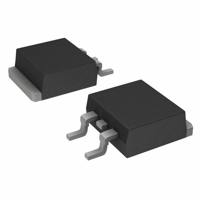
TO-263/D2PAK
Features
-Batch process design, excellent power dissipation offers
better reverse leakage current and thermal resistance.
-Low profile surface mounted application in order to
0.413(10.50)
0.394(10.00)
0.059(1.50)
0.031(0.80)
optimize board space.
-Low power loss, high efficiency.
-High current capability, low forward voltage drop.
-High surge capability.
-Guardring for overvoltage protection.
-Ultra high-speed switching.
-Silicon epitaxial planar chip, metal silicon junction.
-Lead-free parts meet environmental standards of
0.185(4.70)
0.169(4.30)
0.055(1.40)
0.047(1.20)
4
0.370(9.40)
0.327(8.30)
1
2
3
0.114(5.30)
0.098(4.40)
MIL-STD-19500 /228
0.205(5.20)
0.189(4.80)
Mechanical data
-Epoxy: U/L 94-V0 rate flame retardant.
-Case: TO-263/D2PAK, Transfer Molded.
-Terminals: Solderable per MIL-STD-202,
2=4
0.024(0.60)
0.014(0.35)
0.063(1.60)
0.055(1.30)
0.106(2.70)
0.091(2.30)
Dimensions in inches and (millimeters)
method 208.
-Polarity: As marked.
-Weunting Position: Any
-Weight:1.46 gram(approx.).
3
Maximum Ratings (At Ta=25
O
C, unless otherwise noted)
Symbol
CDBD
8060-G
CDBD
8100-G
Unit
Maximum Recurrent peak reverse voltage
VRRM
60
100
V
Maximum RMS voltage
VRMS
42
70
V
Maximum DC blocking voltage
VDC
60
100
V
Parameter
Forward rectified current (See fig. 1)
IO
Maximum forward voltage at IO
VF
Forward surge current, 8.3ms single half sine-wave superimposed on
rated load (JEDEC method)
IFSM
175
A
Maximum Reverse current at 25°C per leg (Note1)
IR
5.0
mA
Maximum Reverse current at 100°C per leg (Note1)
IR
50
mA
Typical Thermal resistance junction to case Per Leg
RθJC
4.0
°C/W
TJ
-55 to +150
°C
TSTG
-55 to +150
°C
Operating temperature range
Storage temperature range
8.0
0.75
A
0.85
V
Notes: 1. Pulse Test: 300µS pulse width, 1% duty cycle.
REV:A
Page 1
QW-BB047
Comchip Technology CO., LTD.
�Comchip
Chip Schottky Barrier Rectifier
SMD Diode Specialist
RATING AND CHARACTERISTIC CURVES (CDBD8060-G Thru. CDBD8100-G)
FIG.1- Forward Derating Curve
FIG.2-Peak Forward Surge Current
300
8
Peak Forward Surge Current ,(A)
Average Firward Rectified Current ,(A)
9
7
6
5
4
3
2
250
200
150
100
50
1
0
0
20
40
60
80
0
100 120 140 160 180 200
1
10
100
Case Temperature, (°C)
Number of Cycles at 60Hz
FIG.3-Typical Forward Characteristic Per Leg
FIG.4-Typical Reverse Characteristics
100
10
Instantaneous Reverse Current, (mA)
Instantaneous Forward Current, ( A )
TJ=125 °C
CDBD8060-G
10
CDBD8100-G
1.0
1.0
TJ=75 °C
0.1
TJ=25 °C
0.01
CDBD8060-G
CDBD8100-G
0.1
0.1
0.3
0.5
0.7
0.9
Instantaneous Forward Voltage, ( V )
1.1
0.001
0
20
40
60
80
100
120
140
Peraent of Rated Voltage Peak Reverse Voltage, (%)
REV:A
Page 2
QW-BB047
Comchip Technology CO., LTD.
�Comchip
Chip Schottky Barrier Rectifier
SMD Diode Specialist
Marking Code
Marking Code
Part Number
CDBD8060-G
SD8L60
CDBD8100-G
SD8L100
XXXXXX
XXXXXX / XXXXXXX = Product type marking code
Suggested PAD Layout
TO-263 / D2PAK
X1
SIZE
(mm)
(inch)
A
9.50
0.374
B
2.50
0.098
C
16.90
0.665
Y1
C
A
X1
10.80
0.425
X2
1.10
0.043
Y1
11.40
0.449
Y2
3.50
0.138
Y2
X2
B
Standard Packaging
TUBE PACK
Case Type
TO-263 / D2PAK
TUBE
BOX
( pcs )
( pcs )
50
2,000
REV: A
Page 3
QW-BB047
Comchip Technology CO., LTD.
�
很抱歉,暂时无法提供与“CDBD8060-G”相匹配的价格&库存,您可以联系我们找货
免费人工找货