SMD Schottky Barrier Diode
SMD Diodes Specialist
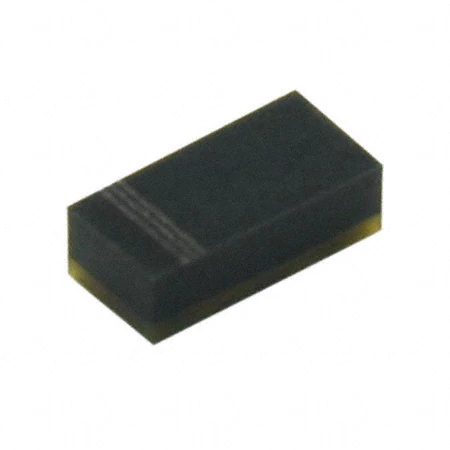
CDBF0320/0330/0340-HF
(RoHS Device)
I O = 3 50 mA V R = 2 0 to 40 Volts Features
Halogen free. L ow forward voltage. Designed for mounting on small surface. Extremely thin / leadless package. Majority carrier conduction.
1005(2512)
0.102(2.60) 0.095(2.40)
0.051(1.30) 0.043(1.10)
Mechanical data
C ase: 1005(2512) standard package, molded plastic. Terminals: Gold plated, solderable per MIL-STD-750,method 2026. Marking code: CDBF0320-HF : BH CDBF0330-HF : BJ CDBF0340-HF : BK Mounting position: Any Weight: 0.006 gram(approx.).
0.035(0.90) 0.027(0.70)
0.020(0.50) Typ.
0.012 (0.30) Typ.
0.040(1.00) Typ.
Dimensions in inches and (millimeter)
Maximum Rating ( at T A =25 C unless otherwise noted)
O
Parameter
Repetitive Peak reverse voltage Reverse voltage RMS reverse voltage Average forward rectified current Forward current, surge peak 8.3 ms single half sine-wave Power dissipation Thermal resistance junction to ambient air Storage temperature Junction temperature
Symbol
V RRM VR V R(RMS) IO I FSM PD R
JA
CDBF0320
20 14
CDBF0330
30 21 350 1.5 200 500 -65 TO +125 + 125
CDBF0340 Unit
40 28 V V mA A mW
O
C/W
O
T STG Tj
O
C C
O
Electrical Characteristics ( at T A =25 C unless otherwise noted)
Parameter
Reverse current CDBF0320-HF CDBF0330-HF CDBF0340-HF Forward voltage V R = 1 0V V R = 2 0V V R = 3 0V I F = 2 0mA I F = 2 00mA f = 1 MHz, and 0 VDC reverse voltage I F =I R =10mA,Irr=0.1xIR,RL=100 ohm
Conditions
Symbol Min Typ Max Unit
IR 5 5 5 0.37 0.60 50 6.4 uA
VF CT T rr
V pF nS
REV:A
Capacitance between terminals Reverse recovery time
QW-G1078
Page 1
Comchip Technology CO., LTD.
�S MD Schottky Barrier Diode
SMD Diodes Specialist
RATING AND CHARACTERISTIC CURVES (CDBF0320/0330/0340-HF)
F ig. 1 - Forward characteristics
1 000 1m
125 C
O
Fig. 2 - Reverse characteristics
Reverse current ( A )
Forward current (mA )
1 00
100u
10
1 0u
75 C
O
1
1u
25 C
O
C
O
0.1
C
125
C
75
25
0.01 0 0.1 0.2 0.3 0.4 0.5 0.6
-25
C
O
100n
O
O
10n 0 10 20 30 40
Forward voltage (V)
Reverse voltage (V)
Fig.3 - Capacitance between terminals characteristics
Capacitance between terminals ( P F)
50
120
Fig.4 - Current derating curve
Average forward current(%)
f=1MHz O T A =25 C
40
Mounting on glass epoxy PCBs
100
80
30
60
20
40
10
20
0 0 10 20 30 40
0
0 25 50 75 100
O
125
150
Reverse voltage (V)
Ambient temperature ( C)
REV:A
QW-G1078
Page 2
Comchip Technology CO., LTD.
�S MD Schottky Barrier Diode
SMD Diodes Specialist
Reel Taping Specification
P0 P1 d Index hole E T
F B
Polarity
W C
P
A
12 0
o
D2
D1 D
W1
Trailer ....... .......
10 pitches (min)
Device ....... ....... ....... .......
Leader ....... .......
10 pitches (min)
End
Start
Direction of Feed
SYMBOL
A
1.55 ± 0.10
0.061 ± 0.004
B
2.65 ± 0.10
0.104 ± 0.004
C
1.05 ± 0.10
0.041 ± 0.004
d
1.55 ± 0.05
0.061 ± 0.002
D
178 ± 1
7.008 ± 0.04
D1
60.0 MIN.
2.362 MIN.
D2
13.0 ± 0.20
0.512 ± 0.008
F/1005
(mm) (inch)
SYMBOL
E
1.75 ± 0.10
0.069 ± 0.004
F
3.50 ± 0.05
0.138 ± 0.002
P
4.00 ± 0.10
0.157 ± 0.004
P0
4.00 ± 0.10
0.157 ± 0.004
P1
2.00 ± 0.05
0.079 ± 0.004
T
0.23 ± 0.05
0.009 ± 0.002
W
8.00 ± 0.20
0.315 ± 0.008
W1
13.5 MAX.
0.531 MAX.
F/1005
(mm) (inch)
REV:A
QW-G1078
Page 3
Comchip Technology CO., LTD.
�S MD Schottky Barrier Diode
SMD Diodes Specialist
Marking Code
Park Number CDBF0320-HF CDBF0330-HF CDBF0340-HF Marking Code
BH BJ BK
XX
xx = Product type marking code
Suggested PAD Layout
F/1005 SIZE (mm) A B C D E 2.10 1.20 1.20 3.30 0.90 (inch) 0.083 0.047 0.047
C D A E
0.130
B
0.035
Standard Package
Qty per Reel Case Type (Pcs) F/1005 4000 Reel Size (inch) 7
REV:A
QW-G1078
Page 4
Comchip Technology CO., LTD.
�
很抱歉,暂时无法提供与“CDBF0320-HF”相匹配的价格&库存,您可以联系我们找货
免费人工找货