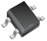
Low VF Schottky Bridge Rectifiers
COMCHIP
SMD DIODE SPECIALIST
CDBHD120L-G Thru 1100L-G
R everse Voltage: 20 - 100 Volts Forward C urrent: 1.0 Amp
• Low Vf S chottky barrier chips in bridge • Metal-Semiconductor junction with guard ring • High s urge current capability • Silicon epitaxial planar chips • For use in low voltage, high efficiency inverters, free wheeling, and polarity protection applications • Lead-free part, meet RoHS requirements
+
~
F eatures
–
Mini-DIP
.106(2.7) .090(2.3)
~
C .02(0.5) .043(1.1) .027(0.7)
~ +
~ –
.031(0.8) .019(0.5)
.165(4.2) .150(3.8)
.275(7.0) Max.
Mechanical Data
• Case: Mini-Dip bridge (TO-269AA) plastic molded case • Epoxy: UL94-V0 rated flame retardant • Terminals: Solderable per MIL-STD-750 Method 2026 • Polarity: As marked on body • Mounting Position: Any • Weight: 0.0078 ounces, 0.22 grams
.193(4.90) .177(4.50)
.067(1.7) .057(1.3)
.016(0.41) .006(0.15) .051(1.3) .035(0.9)
.106(2.7) .090(2.3) .008(0.2) Max.
.114(2.90) .094(2.40)
Unit :inch(mm)
MAXIMUM RATING AND ELECTRICAL CHARACTERISTICS
Ratings at 25°C ambient temperature unless otherwise specified
C DBHD - S ymbols Maximum Recurrent Peak Reverse Voltage M aximum RMS Voltage Maximum DC Blocking Voltage Maximum Average Forward Rectified Current 0.2x0.2” (5.0x5.0mm) copper pad area, s ee Figure 1 Peak Forward Surge Current
8.3mS single half sine-wave superimp osed on rated load (JEDEC Me thod)
1 20L 20 14 20
1 40L 40 28 40
1 60L 60 42 60
1 80L 80 56 80
11 0 0L 100 70 100
U nits Volts Volts Volts
V RRM V RMS V DC
I AV
1 .0
Amps
I FSM
VF
IR
3 0.0 0 . 44 0 . 62 5 0.5 20.0
2 50 125
Amps 0. 75
Volts
mA
Maximum Forward Voltage at 1.0A (Note 1) Maximum DC Reverse Current at Rated DC Blocking Voltage Typical Junction Capacitance (Note 2) Typical Thermal Resistance (Note 3) O perating Junction Temperature Range S torage Temperature Range
: Note 1 . Pulse test: 300µS pu lse wi dth, 1% du ty cy cle
T A = 2 5°C T A = 100 °C
CJ R θ JA R θ JL TJ T STG
pF
8 5.0 2 0.0 - 55 ~ +125 - 55 ~ +150
° C/W °C °C
2. Me asured at 1.0MH z an d ap plied reverse vo ltage of 4.0 Volts 3. Therma l resistance from junction to am bient and from junction to lead P.C.B. mo unted on 0. 2x0.2”(5.0x5.0mm ) co pper pa d ar eas.
Page 1
MDS0702004A
�Low VF Schottky Bridge Rectifiers
Fig.1 - Forward Current Derating Curve P eak Forward Surge Current (A) Average Forward Current (A)
1.2 1.0 0.8 0.6 0.4 0.2
CDBHD 12 0L-G - 1 6 0L-G CDBHD 18 0L-G - 11 0 0 L-G single phase half wave 60Hz resistive or inductive load 3.75”(9.5mm) lead length
COMCHIP
SMD DIODE SPECIALIST
Fig. 2 - Maximum Non-Repetitive Peak Forward Surge Current
100
10
T L =110°C 8.3mS single half sine-wave (JEDEC Method)
1 1 10 100
0
25
50
75
100
125
150
175
L ead Temperature ( °C)
N umber of Cycles at 60 Hz
10
Instantaneous Reverse Current (mA)
Fig. 3 - Typical Instantaneour Forward Characteristics Instantaneous Forward Current (A)
pulse width =300µS 1% duty cycle, T j =25°C
Fig. 4A - Typical Reverse Characteristics
100
CDBHD 12 0L-G - 1 6 0L-G
10 T J =125°C 1.0 T J =75°C 0.1
1.0
CDBHD 12 0L-G - 1 4 0L-G
0.1
CDBHD 16 0L-G
0.01
T J =25°C
CDBHD 18 0L-G - 110 0L-G
0.01 0
0.2
0.4
0.6
0.8
1.0
0.001 0
20
40
60
80
100
120
140
Instantaneous Forward Voltage (Volts)
Percent of Rated Peak Reverse Voltage ( %)
Fig. 5 - Typical Junction Capacitance
1000
Fig. 4B - Typeical Reverse Characteristic Instantaneous Reverse Current (µA)
1000
CDBHD180L-G - 1100L-G
T J =25°C f=1.0MHz
Junction Capacitance (pF)
100
T J =150°C T J =125°C
CDBHD 12 0L-G - 1 4 0L-G
10 1.0 T J =100°C
100
CDBHD16 0L-G CDBHD 18 0L-G - 110 0L-G
0.1 T J =25°C 0.01 0 20 40 60 80 100
10 0 .1
1.0
10
100
Reverse Voltage (Volts)
MDS0702004A
Percent of Rated Peak Reverse Voltage ( %)
Page 2
�
很抱歉,暂时无法提供与“CDBHD160L-G”相匹配的价格&库存,您可以联系我们找货
免费人工找货