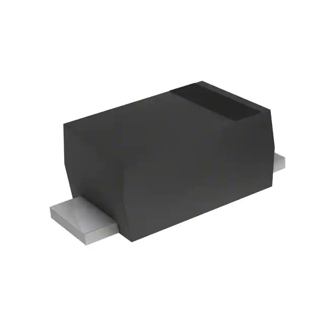
SMD Schottky Barrier Diodes
CDBW0520L-HF Thru. CDBW0540-HF
Reverse Voltage: 20 to 40 Volts
Forward Current: 0.5 Amp
RoHS Device
Halogen Free
SOD-123
Features
-Low turn on voltage.
-Fast switching.
-PN junction guard ring for transient and ESD
protection.
0.110(2.80)
0.098(2.50)
0.071(1.80)
0.055(1.40)
0.028(0.70)
0.019(0.50)
Mechanical data
0.154(3.90)
0.141(3.60)
-Case: SOD-123, molded plastic.
-Terminals: solderable per MIL-STD-750,
method 2026.
-Polarity: Color band denotes cathode end.
0.053(1.35)
0.037(0.95)
0.008(0.20)
Max.
Marking
0.016(0.40)
Min.
0.005(0.12)
Max.
-Weight: 0.0097 gram(approx.).
Circuit Diagram
CDBW0520L-G: SD
Dimensions in inches and (millimeter)
CDBW0530-G: SE
CDBW0540-G: SF
Maximum Ratings and Electrical Characteristics (At Ta=25°C, unless otherwise noted)
Parameter
Symbol
CDBW0520L-HF
CDBW0530-HF
CDBW0540-HF
Units
Max. repetitive peak reverse voltage
VRRM
20
30
40
V
Max. DC blocking voltage
VDC
20
30
40
V
Max. RMS voltage
VRMS
14
21
28
V
Peak surge forward current, 8.3ms
single half sine-wave superimposed
on rate load (JEDEC method)
IFSM
5.5
A
Max. average forward current
IO
0.5
A
Max. forward voltage
VF
0.3@IF=0.1A
0.385@IF=0.5A
0.375@IF=0.1A
0.430@IF=0.5A
0.51@IF=0.5A
0.62@IF=1.0A
V
Max. reverse current
IR
0.075@VR=10V
0.25@VR=20V
0.02@VR=15V
0.13@VR=30V
0.01@VR=20V
0.02@VR=40V
mA
Max. thermal resistance (Note 1)
Max. operating junction temperature
Storage temperature
RθJA
RθJL
206
150
°C/W
TJ
125
°C
TSTG
-55 to +125
°C
Notes: 1. Thermal resistance from junction to ambient and junction to lead, mounted on P.C.B. with 0.2×0.2 inch copper pad area.
2
Company reserves the right to improve product design , functions and reliability without notice.
REV:A
Page 1
QW-JB010
Comchip Technology CO., LTD.
�SMD Schottky Barrier Diodes
RATING AND CHARACTERISTIC CURVES (CDBW0520L-HF thru CDBW0540-HF)
Fig.1 Forward Characteristics
Fig.2 Current Derating Curve
10
A v e ra ge Rec t ifi e d Curr e n t(A )
1.2
F o r w a rdC u rr e n t (A )
CDBW0540-HF
1
CDBW0520L-HF
0.1
CDBW0530-HF
0.01
Mounted on glass
epoxy PCB
1.0
0.8
0.6
0.4
0.2
0
0
0.2
0.4
0.6
0.8
1.0
0
Forward voltage (V)
25
50
75
100
125
150
Lead Temperature (°C)
Fig.3 Total Capacitance vs. Reverse
voltage
1000
To ta lC a p a c i ta n c e ( p F )
f=1.0MHz
100
10
1
0.1
0
5
10
15
20
25
Reverse Voltage (V)
Company reserves the right to improve product design , functions and reliability without notice.
REV:A
Page 2
QW-JB010
Comchip Technology CO., LTD.
�SMD Schottky Barrier Diodes
Reel Taping Specification
d
P0
P1
T
E
Index hole
F
W
B
Polarity
P
C
A
12
o
0
D2
D1 D
W1
Trailer
.......
.......
End
Device
.......
.......
Leader
.......
.......
.......
.......
10 pitches (min)
Start
10 pitches (min)
Direction of Feed
SOD-123
SOD-123
SYMBOL
A
B
C
d
D
D1
D2
(mm)
1.90 ± 0.10
4.00 ± 0.10
1.50 ± 0.10
1.55 ± 0.10
178 ± 1.00
50.0 MIN.
13.0 ± 0.20
(inch)
0.075 ± 0.04
0.157 ± 0.04
0.059 ± 0.04
0.061 ± 0.04
7.00 ± 0.039
1.968 MIN.
0.512 ± 0.079
SYMBOL
E
F
P
P0
P1
W
W1
(mm)
1.75 ± 0.10
3.50 ± 0.05
4.00 ± 0.10
4.00 ± 0.10
2.00 ± 0.05
8.00 ± 0.30
14.4 MAX.
(inch)
0.069 ± 0.004
0.138 ± 0.002
0.157 ± 0.004
0.157 ± 0.004
0.079 ± 0.002
0.315 ± 0.011
0.567 MAX
Company reserves the right to improve product design , functions and reliability without notice.
REV:A
Page 3
QW-JB010
Comchip Technology CO., LTD.
�SMD Schottky Barrier Diodes
Marking Code
Part Number
Marking Code
CDBW0520L-HF
SD
CDBW0530-HF
SE
CDBW0540-HF
SF
XX
xx = Product type marking code
Suggested PAD Layout
D
SOD-123
A
SIZE
(mm)
(inch)
E
A
3.24
0.128
B
0.80
0.032
C
1.00
0.039
D
4.04
0.159
E
2.44
0.096
C
B
Standard Packaging
REEL PACK
Case Type
SOD-123
REEL
Reel Size
( pcs )
(inch)
3,000
7
Company reserves the right to improve product design , functions and reliability without notice.
REV:A
Page 4
QW-JB010
Comchip Technology CO., LTD.
�
很抱歉,暂时无法提供与“CDBW0540-G”相匹配的价格&库存,您可以联系我们找货
免费人工找货