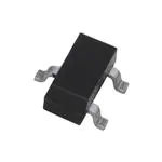
Surface Mount Switching Diode
CDST7000-G
Voltage: 100 Volts
Current: 200 mA
Features
SOT-23
Fast Switching Speed
Surface Mount Package Ideally Suited for
Automatic Insertion
For General Purpose Switching Applications
High Conductance
.119 (3.0)
.110 (2.8)
.020 (0.5)
Top View
.056 (1.40)
.047 (1.20)
3
Mechanical data
1
ANODE
3
CATHODE/ANODE
2
CATHODE
2
.020 (0.5)
.044 (1.10)
.035 (0.90)
.037(0.95) .037(0.95)
.006 (0.15)
.002 (0.05)
1
.006 (0.15)max.
Case: SOT-23, Plastic
Terminals: Solderable per MIL-STD-750,
Method 208
Approx. Weight: 0.008 gram
.103 (2.6)
.086 (2.2)
.020 (0.5)
Dimensions in inches (millimeters)
Maximum Ratings
Rating
Continuous Reverse Voltage
Peak Forward Current
Peak Forward Surge Current
Symbol
VR
Value
100
Units
VDC
IF
200
mAdc
IFM (surge)
500
mAdc
Symbol
Max
Units
Thermal Characteristics
Characteristic
Total Device Dissipation FR– 5 Board(1)
T A = 25°C
Derate above 25°C
Thermal Resistance, Junction t o Ambient
Total Device Dissipation Alumina S ubstrate,(2) T A = 25°C
Derate above 25°C
PD
RθJA
PD
225
mW
1.8
mW/°C
556
°C/W
300
mW
2.4
mW/°C
RθJA
417
°C/W
TJ, Tstg
–55 to +150
°C
Symbol
V(BR)
Min
Max
Units
100
-
Vdc
IR
-
1
VR = 100 Vdc
IR2
-
3
VR = 50 Vdc, 125°C
IR3
-
100
Thermal Resistance, Junction t o Ambient
Junction and Storage Temperature
Electrical Characterics (TA = 25°C unless otherwise noted)
Characteristic (OFF CHARACTERISTICS)
Reverse Breakdown Voltage ( I (BR) = 100 uAdc )
Reverse Voltage Leakage Current
Forward Voltage
V R = 50 Vdc
IF = 1.0 mAdc
IF = 10 mAdc
VF
IF = 100 mAdc
Reverse Recovery Time (I F = IR = 10 mAdc) (Figure 1)
Trr
Diode Capacitance (V R = 0)
C
1.FR–5 = 1.0 X 0.75X 0.062 in.
MDS0301004A
0.55
0.7
0.67
0.82
0.75
1.1
-
uAdc
Vdc
4.0
nS
1.5
pF
2.Alumina = 0.4X 0.3X 0.024 in. 99.5% alumina.
Page 1
�Surface Mount Switching Diode
Rating and Characteristic Curves (CDST7000-G)
820 Ω
+10 V
2k
0.1 µF
tp
tr
IF
100 µH
0.1 µF
IF
t
trr
10%
t
DUT
50 Ω Οutput
Pulse
Generator
50 Ω Input
Sampling
Oscilloscope
90%
IR(REC) = 1 mA
IR
VR
Output Pulse
(IF = IR = 10 mA; measured
at IR(REC) = 1 mA)
Input Signal
Notes: 1. A 2.0 kΩ variable resistor adjusted for a Forward Current (IF) of 10 mA.
Notes: 2. Input pulse is adjusted so IR(peak) is equal to 10 mA.
Notes: 3. tp » trr
Figure 1. Recovery Time Equivalent Test Circuit
10
100
10
IR, Reverse Current(µA)
TA = 85°C
TA = –40°C
VR
TA = 25°C
1.0
TA = 125°C
1.0
TA = 85°C
0.1
TA = 55°C
0.01
TA = 25°C
0.1
0.2
0.4
0.6
0.8
1.0
0.001
1.2
0
10
20
30
VF, Forward Voltage(V)
VR, Reverse Voltage(V)
Figure 2. Forward Voltage
Figure 3. Leakage Current
40
50
0.68
CD, Diode Capacitance(PF)
I F, Forward Current (mA)
TA = 150°C
0.64
0.60
0.56
0.52
0
2.0
4.0
6.0
8.0
VR, Reverse Voltage(V)
Figure 4. Capacitance
MDS0301004A
Page 2
�
很抱歉,暂时无法提供与“CDST-7000-G”相匹配的价格&库存,您可以联系我们找货
免费人工找货