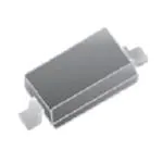
SMD Switching Diode
CDSV4148-G
RoHS Device
SOD-323
Features
- Fast Switching Speed
0.106 (2.75)
0.098 (2.55)
- High Conductance
0.014 (0.35)
0.010 (0.25)
- Surface Mount Package Ideally Suited for
Automatic Insertion
0.055 (1.40)
0.047 (1.20)
0.071 (1.80)
0.063 (1.60)
- For General Purpose Switching Appilcations.
0.006 (0.150)
0.003 (0.080)
0.040 (1.00)
Mechanical data
Max.
0.004 (0.10)max
- Case: SOD-323, Molded Plastic
0.019 (0.475)REF
- Terminals: Solderable per MIL-STD-202, Method208
Dimensions in inches and (millimeter)
- Mounting position: Any.
Circuit Diagram
Maximum Ratings (at T =25°C unless otherwise noted)
A
Symbol
Value
Unit
Non-Repetitive peak reverse voltage
VRM
100
V
Peak repetitive peak reverse voltage
Working peak reverse voltage
DC blocking voltage
VRRM
VRWM
VR
100
V
VR(RMS)
71
V
Forward continuous current
IFM
300
mA
Average rectified output current
Io
150
mA
IFSM
2.0
A
PD
200
mW
RθJA
625
°C/W
Junction temperature range
Tj
-40 ~ +150
°C
Storage temperature range
TSTG
-55 ~ +150
°C
Parameter
RMS reverse voltage
Non-Repetitive peak forward surge current @ t=8.3ms
Power dissipation
Thermal resistance from junction to ambient
Electrical Characteristics (at T =25°C unless otherwise noted)
A
Parameter
Conditions
Symbol
Min
Typ
Max
Unit
V
Forward voltage
IF1 = 1mA
IF2 = 10mA
IF3 = 50mA
IF4 = 150mA
VF
0.715
0.855
1.0
1.25
Reverse current
VR = 75 V
VR = 20 V
IR
1
25
uA
nA
Capacitance between terminals
VR = 0V, f = 1MHZ
CT
2
PF
Reverse recovery time
IF = IR = 10mA, RL =100 Ω, Irr = 0.1 X IR
TRR
4
nS
Company reserves the right to improve product design , functions and reliability without notice.
REV:B
Page 1
QW-B0047
Comchip Technology CO., LTD.
�SMD Switching Diode
PATING AND CHARACTERISTIC CURVES (CDSV4148-G)
Fig.1 - Forward Characteristics
Fig.2 - Reverse Characteristics
1000
200
100
Reverse Current, IR (nA)
0°
C
=1
0
10
TA=
25
°C
TA
Forward Current, IF (mA)
TA=100°C
1
0.1
0.01
100
10
TA=25°C
1.0
0
0.2
0.4
0.6
0.8
1.0
0
1.2
10
20
Forward Voltage, VF (V)
40
50
60
70
80
Reverse Voltage, VR (V)
Fig.3 - Capacitance Characteristics
Fig.4 - Power Derating Curve
1.2
300
TA=25°C
f=1MHz
Power Dissipation, PD (mW)
Capacitance Between Terminals, CT (pF)
30
1.1
1.0
0.9
250
200
150
100
50
0
0.8
0
5
10
15
20
0
Reverse Voltage, VR (V)
25
50
75
100
125
150
Ambient Temperature, TA (°C)
Company reserves the right to improve product design , functions and reliability without notice.
REV:B
Page 2
QW-B0047
Comchip Technology CO., LTD.
�SMD Switching Diode
Reel Taping Specification
d
P0
P1
T
E
Index hole
F
W
B
P
C
A
12
o
0
D2
D1 D
W1
Trailer
Device
.......
.......
End
.......
.......
Leader
.......
.......
160mm (min)
.......
.......
Start
400mm (min)
Direction of Feed
SOD-323
SOD-323
SYMBOL
A
B
C
d
D
D1
D2
(mm)
1.46 ± 0.05
2.90 ± 0.05
1.25 ± 0.05
1.50 + 0.10
178.00 ± 2.00
54.40 ± 1.00
13.00 ± 1.00
(inch)
0.057 ± 0.002
0.114 ± 0.002
0.049 ± 0.002
0.059 + 0.004
7.008 ± 0.079
2.142 ± 0.039
0.512 ± 0.039
SYMBOL
E
F
P
P0
P1
W
W1
(mm)
1.75 ± 0.10
3.50 ± 0.10
4.00 ± 0.10
4.00 ± 0.10
2.00 ± 0.10
8.00 + 0.30 / - 0.10
12.30 ± 1.00
(inch)
0.069 ± 0.004
0.138 ± 0.004
0.158 ± 0.004
0.158 ± 0.004
0.079 ± 0.004 0.315 + 0.012 / - 0.004
Company reserves the right to improve product design , functions and reliability without notice.
0.484 ± 0.039
REV:B
Page 3
QW-B0047
Comchip Technology CO., LTD.
�SMD Switching Diode
Marking Code
Part Number
Marking Code
CDSV4148-G
T4
T4
Suggested PAD Layout
SOD-323
SIZE
D
(mm)
(inch)
A
2.15
0.085
B
0.80
0.031
C
0.70
0.028
D
2.95
0.116
E
1.35
0.053
A
E
C
B
Standard Packaging
REEL PACK
Case Type
SOD-323
REEL
Reel Size
( pcs )
(inch)
3,000
7
Company reserves the right to improve product design , functions and reliability without notice.
REV:B
Page 4
QW-B0047
Comchip Technology CO., LTD.
�
很抱歉,暂时无法提供与“CDSV4148-G”相匹配的价格&库存,您可以联系我们找货
免费人工找货