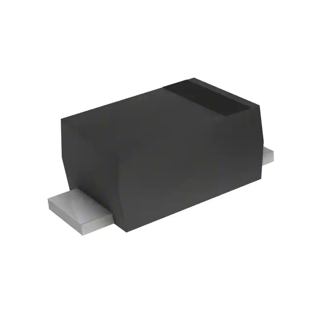
Small Signal Switching Diodes
CDSW4448-G
Reverse Voltage: 75 Volts
Power Dissipation: 400 mW
RoHS Device
SOD-123
Features
-Design for mounting on small surface.
-High speed switching.
0.110(2.80)
0.098(2.50)
-High mounting capability, strong surge
withstand, high reliability.
0.071(1.80)
0.055(1.40)
0.028(0.70)
0.019(0.50)
-Also available in other standard case:
CDSN4448 - 1206 size
CDSF4448 - 1005 size
CDSU4448 - 0603 size
0.154(3.90)
0.141(3.60)
Mechanical data
0.053(1.35)
0.037(0.95)
0.008(0.20)
Max.
-Case: SOD-123, molded plastic.
0.016(0.40)
Min.
0.005(0.12)
Max.
-Terminals: solderable per MIL-STD-750,
method 2026.
-Polarity: indicated by cathode band.
Dimensions in inches and (millimeter)
-Approx. weight: 0.01 grams
Maximum Ratings and Electrical Characteristics
(at Ta=25°C unless otherwise noted)
Value
Units
VRRM
75
V
Reverse voltage
VR
75
V
Forward current
IFM
500
mA
Peak surge forward current
IFSM
4
A
Power dissipation
PD
400
mW
0.72
0.855
1
1.25
V
2.5
0.025
μA
Parameter
Repetitive peak reverse voltage
Symbol
Conditions
T=1.0 μS
Maximum forward voltage
VF
@IF=5mA
@IF=10mA
@IF=100mA
@IF=150mA
Maximum reverse current
IR
@VR=75V
@VR=25V
Maximum reverse recovery time
Trr
IF=10mA, RL=100Ω
4
nS
Typical diode capacitance
CJ
VR=0V, f=1.0MHz
4
pF
Maximum junction temperature
TJ
125
O
C
TSTG
-55 to +125
O
C
Storage temperature
REV:A
Page 1
QW-B0013
Comchip Technology CO., LTD.
�Small Signal Switching Diodes
RATING AND CHARACTERISTIC CURVES (CDSW4448-G)
Fig.1 - Forward Characteristics
Fig.2 - Reverse Characteristics
10μ
100
10
O
TA=85 C
TA=-30 OC
TA=0 OC
O
TA=50 C
1
Reverse Current, (A)
Forward Current, (mA)
1μ
O
TA=75 C
10n
TA=25 OC
TA=0 OC
O
TA=25 C
1n
0.1
O
TA=-30 C
0.1n
0
0.2
0.4
0.6
0.8
1.0
20
0
40
80
60
Forward Voltage, (V)
Reverse Voltage, (V)
Fig.3 - Capacitance Between Terminals
Characteristics
Fig.4 - Power Derating Curve
4
100
600
Mounted on glass
epoxy PCBs
O
TJ=25 C
f=1MHz
Power Dissipation, (mW)
Capacitance Between Terminals, (pF)
TA=125 OC
100n
3
2
1
500
400
300
200
100
0
0
0
1
2
3
4
5
6
0
25
50
75
100
125
150
175
Ambient Temperature, (°C)
Reverse Voltage, (V)
REV:A
Page 2
QW-B0013
Comchip Technology CO., LTD.
�
很抱歉,暂时无法提供与“CDSW4448-G”相匹配的价格&库存,您可以联系我们找货
免费人工找货