CX84100-41/-23 SCXV.22bis Modem
V.22bis Modem with CX20493 SmartDAA®
Line Side Device
Data Sheet
Doc. No. 102339D
January 17, 2012
�CX84100-41/-23 SCXV.22bis Modem Data Sheet
Revision Record
Revision
D
C
B
A
Date
1/17/2012
3/3/2004
12/9/2003
12/3/2003
Comments
Rev. D release.
Rev. C release.
Rev. B release.
Initial release.
© 2003, 2004, 2012, Conexant Systems, Inc.
All Rights Reserved.
Information in this document is provided in connection with Conexant Systems, Inc. (“Conexant”) products. These materials are
provided by Conexant as a service to its customers and may be used for informational purposes only. Conexant assumes no
responsibility for errors or omissions in these materials. Conexant may make changes to specifications and product descriptions at
any time, without notice. Conexant makes no commitment to update the information and shall have no responsibility whatsoever for
conflicts or incompatibilities arising from future changes to its specifications and product descriptions.
No license, express or implied, by estoppel or otherwise, to any intellectual property rights is granted by this document. Except as
provided in Conexant’s Terms and Conditions of Sale for such products, Conexant assumes no liability whatsoever.
THESE MATERIALS ARE PROVIDED “AS IS” WITHOUT WARRANTY OF ANY KIND, EITHER EXPRESS OR IMPLIED,
RELATING TO SALE AND/OR USE OF CONEXANT PRODUCTS INCLUDING LIABILITY OR WARRANTIES RELATING TO
FITNESS FOR A PARTICULAR PURPOSE, CONSEQUENTIAL OR INCIDENTAL DAMAGES, MERCHANTABILITY, OR
INFRINGEMENT OF ANY PATENT, COPYRIGHT OR OTHER INTELLECTUAL PROPERTY RIGHT. CONEXANT FURTHER
DOES NOT WARRANT THE ACCURACY OR COMPLETENESS OF THE INFORMATION, TEXT, GRAPHICS OR OTHER ITEMS
CONTAINED WITHIN THESE MATERIALS. CONEXANT SHALL NOT BE LIABLE FOR ANY SPECIAL, INDIRECT, INCIDENTAL,
OR CONSEQUENTIAL DAMAGES, INCLUDING WITHOUT LIMITATION, LOST REVENUES OR LOST PROFITS, WHICH MAY
RESULT FROM THE USE OF THESE MATERIALS.
Conexant products are not intended for use in medical, lifesaving or life sustaining applications. Conexant customers using or selling
Conexant products for use in such applications do so at their own risk and agree to fully indemnify Conexant for any damages
resulting from such improper use or sale.
The following are trademarks of Conexant Systems, Inc.: Conexant® and the Conexant C symbol, and SmartDAA®. Product names
or services listed in this publication are for identification purposes only, and may be trademarks of third parties. Third-party brands
and names are the property of their respective owners.
For additional disclaimer information, please consult Conexant’s Legal Information posted at www.conexant.com, which is
incorporated by reference.
Reader Response: Conexant strives to produce quality documentation and welcomes your feedback. Please send comments and
suggestions to tech.pubs@conexant.com. For technical questions, contact your local Conexant sales office or field applications
engineer.
ii
Conexant
102339D
�CX84100-41/-23 SCXV.22bis Modem Data Sheet
Contents
1. Introduction .......................................................................................................................... 1-1
1.1 Overview ................................................................................................................................................... 1-1
1.2 Features .................................................................................................................................................... 1-3
1.2.1 SmartDAA Features .................................................................................................................... 1-4
1.2.2 Applications ................................................................................................................................ 1-4
1.3 Technical Overview ................................................................................................................................... 1-5
1.3.1 General Description .................................................................................................................... 1-5
1.3.2 MCU............................................................................................................................................ 1-5
1.3.3 Operating Modes ........................................................................................................................ 1-5
1.3.3.1
Data Modes ............................................................................................................... 1-5
1.3.3.2
Worldwide Operation................................................................................................. 1-5
1.3.4 Reference Design ....................................................................................................................... 1-6
1.4 Hardware Description................................................................................................................................ 1-7
1.4.1 CX84100 V.22bis Modem ........................................................................................................... 1-7
1.4.2 Digital Isolation Barrier ................................................................................................................ 1-7
1.4.3 CX20493 SmartDAA Line Side Device ....................................................................................... 1-7
1.5 Commands ................................................................................................................................................ 1-8
2. Technical Specifications....................................................................................................... 2-1
2.1 Serial DTE Interface Operation ................................................................................................................. 2-1
2.1.1 Automatic Speed/Format Sensing .............................................................................................. 2-1
2.2 Establishing Data Modem Connections .................................................................................................... 2-2
2.2.1 Dialing ......................................................................................................................................... 2-2
2.2.2 Modem Handshaking Protocol ....................................................................................................2-2
2.2.3 Call Progress Tone Detection ..................................................................................................... 2-2
2.2.4 Answer Tone Detection............................................................................................................... 2-2
2.2.5 Ring Detection ............................................................................................................................ 2-2
2.2.6 Billing Protection ......................................................................................................................... 2-2
2.2.7 Connection Speeds .................................................................................................................... 2-2
2.2.8 Automode ................................................................................................................................... 2-3
2.3 Data Mode ................................................................................................................................................ 2-3
2.3.1 Speed Buffering (Normal Mode) .................................................................................................2-3
2.3.2 Flow Control................................................................................................................................ 2-3
2.3.3 Direct Mode ................................................................................................................................ 2-3
2.3.4 Escape Sequence Detection....................................................................................................... 2-4
2.3.5 Telephone Line Monitoring ......................................................................................................... 2-4
2.3.6 Retrain ........................................................................................................................................ 2-4
2.3.7 Programmable Inactivity Timer ................................................................................................... 2-4
2.3.8 DTE Signal Monitoring (Serial DTE Interface Only) .................................................................... 2-4
2.4 Error Correction and Data Compression ................................................................................................... 2-4
2.4.1 V.42 Error Correction .................................................................................................................. 2-4
2.4.2 MNP 2-4 Error Correction ........................................................................................................... 2-4
102339D
Conexant
iii
�CX84100-41/-23 SCXV.22bis Modem Data Sheet
2.5
2.6
2.7
2.8
2.4.3 V.42 bis Data Compression ........................................................................................................ 2-5
Telephony Extensions ............................................................................................................................... 2-5
2.5.1 Line In Use Detection.................................................................................................................. 2-5
2.5.2 Extension Pickup Detection ........................................................................................................ 2-5
2.5.3 Remote Hangup Detection.......................................................................................................... 2-5
2.5.4 Digital Line Protection ................................................................................................................. 2-5
Caller ID .................................................................................................................................................... 2-6
2.6.1 Type II CID.................................................................................................................................. 2-6
Worldwide Country Support ...................................................................................................................... 2-6
Diagnostics ............................................................................................................................................... 2-7
2.8.1 Commanded Tests ..................................................................................................................... 2-7
Low Power Mode ...................................................................................................................................... 2-7
2.9
3. Hardware Interface............................................................................................................... 3-1
3.1 CX84100 V.22bis Modem Hardware Pins and Signals ............................................................................. 3-1
3.1.1 CX84100 V.22bis Modem Signal Summary ................................................................................ 3-1
3.1.1.1
CX20493 LSD Interface (Through DIB) ..................................................................... 3-1
3.1.1.2
Call Progress Speaker Interface ............................................................................... 3-1
3.1.1.3
Serial DTE Interface and Indicator Outputs ............................................................... 3-1
3.1.1.4
Control and Signals ................................................................................................... 3-1
3.1.1.5
Crystal/Clock and Power Signals .............................................................................. 3-2
3.1.2 CX84100 V.22bis Modem Pin Assignments and Signal Definitions ............................................ 3-2
3.2 CX20493 LSD 28-Pin QFN Hardware Pins and Signals ........................................................................... 3-8
3.2.1 CX20493 LSD 28-Pin QFN Signal Summary .............................................................................. 3-8
3.2.1.1
CX84100 V.22bis Modem Interface (Through DIB) ................................................... 3-8
3.2.1.2
Telephone Line Interface .......................................................................................... 3-8
3.2.1.3
Voltage References................................................................................................... 3-8
3.2.1.4
General Purpose Input/Output .................................................................................. 3-9
3.2.1.5
No Connects ............................................................................................................. 3-9
3.2.2 CX20493 LSD 28-Pin QFN Pin Assignments and Signal Definitions .......................................... 3-9
3.3 CX20493 LSD 32-Pin LQFP Hardware Pins and Signals ....................................................................... 3-13
3.3.1 CX20493 LSD 32-Pin LQFP Signal Summary .......................................................................... 3-13
3.3.1.1
CX84100 Interface (Through DIB)........................................................................... 3-13
3.3.1.2
Telephone Line Interface ........................................................................................ 3-13
3.3.1.3
Voltage References................................................................................................. 3-13
3.3.1.4
General Purpose Input/Output ................................................................................ 3-14
3.3.1.5
No Connects ...........................................................................................................3-14
3.3.2 CX20493 LSD 32-Pin LQFP Pin Assignments and Signal Definitions ...................................... 3-14
3.4 CX20493 LSD GPIO DC Electrical Characteristics ................................................................................. 3-18
3.5 Electrical and Environmental Specifications ............................................................................................ 3-19
3.5.1 Operating Conditions, Absolute Maximum Ratings, and Power Requirements ........................ 3-19
3.6 Interface Timing and Waveforms ............................................................................................................ 3-21
3.6.1.1
Serial DTE Interface ................................................................................................ 3-21
3.7 Crystal Specifications .............................................................................................................................. 3-22
4. Package Dimensions ........................................................................................................... 4-1
iv
Conexant
102339D
�CX84100-41/-23 SCXV.22bis Modem Data Sheet
Figures
Figure 1-1. SCXV.22bis Modem Simplified Interface Diagram .....................................................................1-2
Figure 1-2. SCXV.22bis Modem Major Interfaces ......................................................................................... 1-2
Figure 3-1. CX84100 V.22bis Modem Hardware Interface Signals ............................................................... 3-2
Figure 3-2. CX84100 V.22bis Modem 28-Pin TSSOP Pin Signals ............................................................... 3-3
Figure 3-3. CX20493 LSD 28-Pin QFN Hardware Interface Signals ............................................................. 3-9
Figure 3-4. CX20493 LSD 28-Pin QFN Pin Signals .................................................................................... 3-10
Figure 3-5. CX20493 LSD 32-Pin LQFP Hardware Interface Signals ......................................................... 3-14
Figure 3-6. CX20493 LSD 32-Pin LQFP Pin Signals .................................................................................. 3-15
Figure 3-7. Waveforms - Serial DTE Interface ............................................................................................ 3-21
Figure 4-1. Package Dimensions - 28-Pin TSSOP ....................................................................................... 4-2
Figure 4-2. Package Dimensions - 28-Pin QFN: Punch Style ....................................................................... 4-3
Figure 4-3. Package Dimensions - 28-Pin QFN: Sawn Style ........................................................................ 4-4
Figure 4-4. Package Dimensions - 32-Pin LQFP .......................................................................................... 4-5
102339D
Conexant
v
�CX84100-41/-23 SCXV.22bis Modem Data Sheet
Tables
Table 1-1. SCXV.22bis Modem Model/Order/Part Numbers......................................................................... 1-2
Table 1-2. Default Countries Supported........................................................................................................ 1-6
Table 1-3. Supported AT Commands ........................................................................................................... 1-8
Table 2-1. +MS Command Automode Connectivity ...................................................................................... 2-3
Table 2-2. Supported Caller ID Types........................................................................................................... 2-6
Table 2-3. Select Low-Power Mode (-SLP) Command Comparison Table ................................................... 2-7
Table 3-1. CX84100 V.22bis Modem 28-Pin TSSOP Pin Signals ................................................................. 3-3
Table 3-2. CX84100 V.22bis Modem Pin Signal Definitions ......................................................................... 3-4
Table 3-3. CX84100 V.22bis Modem I/O Type Definitions............................................................................ 3-7
Table 3-4. CX84100 V.22bis Modem DC Electrical Characteristics .............................................................. 3-7
Table 3-5. CX20493 LSD 28-Pin QFN Pin Signals ..................................................................................... 3-10
Table 3-6. CX20493 LSD 28-Pin QFN Signal Definitions ........................................................................... 3-11
Table 3-7. CX20493 LSD 32-Pin LQFP Pin Signals ................................................................................... 3-15
Table 3-8. CX20493 LSD 32-Pin LQFP Pin Signal Definitions ................................................................... 3-16
Table 3-9. CX20493 LSD GPIO DC Electrical Characteristics.................................................................... 3-18
Table 3-10. CX20493 LSD AVdd DC Electrical Characteristics .................................................................. 3-18
Table 3-11. Operating Conditions ............................................................................................................... 3-19
Table 3-12. Absolute Maximum Ratings ..................................................................................................... 3-19
Table 3-13. Current and Power Requirements ........................................................................................... 3-20
Table 3-14. Crystal Specifications .............................................................................................................. 3-22
Table 4-1. Package Dimensions: 28-Pin QFN: Punch Style and Sawn Style ............................................... 4-4
vi
Conexant
102339D
�CX84100-41/-23 SCXV.22bis Modem Data Sheet
1.
Introduction
1.1
Overview
The Conexant® CX84100-41/-23 SCXV.22bis modem supports up to V.22bis data
modem operation with V.42 and MNP 4 error correction and V.42 bis data compression
over a serial host interface. Major hardware interfaces and signal interfaces are illustrated
in Figure 1-1 and Figure 1-2, respectively.
Conexant’s SmartDAA® technology (patent pending) eliminates the need for a costly
analog transformer, relays, and opto-isolators typically used in discrete DAA
implementation of country-specific modem configurations thereby reducing system
solution cost to a single bill of materials (BOM).
The SmartDAA system-powered DAA operates reliably without drawing power from the
line, unlike line-powered DAAs, which operate poorly when line current is insufficient
due to long lines or poor line conditions. Enhanced features, such as monitoring of local
extension status without going off-hook, are also supported.
Incorporating Conexant’s proprietary Digital Isolation Barrier (DIB) design (patent
pending) and other innovative DAA features, the SmartDAA architecture simplifies
application design, minimizes layout area, and reduces component cost.
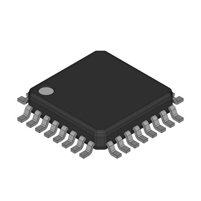
The SCXV.22bis Modem device set, consisting of a CX84100 V.22bis Modem in a 28pin TSSOP package and a CX20493 SmartDAA Line Side Device (LSD) in either a 28pin Quad Flat No-lead (QFN) package or a 32-pin Low Profile Quad Pack (LQFP)
package, supports data operation with hardware-based modem controller, digital signal
processing, and DAA/telephone line interface functions.
The CX84100 V.22bis Modem integrates microcontroller (MCU), serial host interface,
ROM code, RAM, and SmartDAA system side device (SSD) functions onto a single die.
Small, low profile packages, low voltage operation, and low power consumption make
this device set an ideal V.22bis solution for embedded applications.
Although the modem operates by executing a mask code from internal ROM and RAM, a
country profile can be added or modified via host upload to the modem internal RAM.
In V.22 fast connect mode, the modem can connect at 1200 bps with a very short training
time, which is very efficient for small data transfers. Also, V.80 synchronous access
mode supports host-controlled communication protocols.
This data sheet describes the modem capabilities. Commands and parameters are defined
in the Commands Reference Manual (Doc. No. 102338).
102339D
Conexant
1-1
�CX84100-41/-23 SCXV.22bis Modem Data Sheet
Table 1-1. SCXV.22bis Modem Model/Order/Part Numbers
Model/Order/Part Numbers
Marketing Name
Device Set Order No.
SCXV22bis
SCXV22bis Pb Free
DS22-L100-041
DS22-L100-023
Marketing Name
Device Set Order No.
SCXV22bis
SCXV22bis Pb Free
DSCX-V22-041
DSCX-V22LF-023
Modem
[28-Pin TSSOP]
Part No.
CX84100-41
CX84100-23
Line Side Device (LSD)
[28-Pin QFN]
Part No.
CX20493-21
CX20493-31
Modem
[28-Pin TSSOP]
Part No.
CX84100-41
CX84100-23
Line Side Device (LSD)
[38-Pin LQFP]
Part No.
CX20493-25
CX20493-35
Figure 1-1. SCXV.22bis Modem Simplified Interface Diagram
28.224 MHz
Crystal or
Clock
Serial Port
CX84100
V.22bis
Modem
28-Pin TSSOP
Digital
Isolation
Barrier (DIB)
CX20493
SmartDAA 3
Line Side
Device (LSD)
28-Pin QFN or
32-Pin LQFP
Telephone
Line
Interface
Discrete
Components
TIP
RING
Speaker
102339_001
Figure 1-2. SCXV.22bis Modem Major Interfaces
OEM
Supplied
Hardware
Conexant Modem Hardware Devices
28.224 MHz
Crystal or
Clock
DAA Hardware
CX84100
V.22bis Modem
28-Pin TSSOP
Serial
Interface
Serial
Interface
RAM
MCU
SmartDAA
Interface
CX20493 SmartDAA 3
Line Side Device (LSD)
28-Pin QFN or 32-Pin LQFP
Digital
Isolation
Barrier (DIB)
Components
Rectifier
and Filter
Components
Line
Side
DIB
Interface
(LSDI)
Codec
Telephone
Line
Interface
Telephone
Line Interface
Discrete
Components
TELEPHONE
LINE
TIP
RING
ROM
102339_002
1-2
Conexant
102339D
�CX84100-41/-23 SCXV.22bis Modem Data Sheet
1.2
Features
•
•
•
•
•
•
•
•
•
102339D
Modulations
− ITU-T V.22bis (2400 bps)
− V.22 and Bell 212A (1200 bps)
− V.22 fast connect
− V.21 and Bell 103 (300 bps)
− V.23 1200/75 and 75/1200
− V.23 half duplex (1200 bps)
Error correction and data compression
− V.42 (LAPM) error correction
− MNP2-MNP4 error correction
− V.42 bis data compression
Serial interface
Synchronous data mode
− Asynchronous data mode (normal and direct)
− 10- and 11-bit data
− DTE speeds up to 57600 bps
− AT Command speed sensing from 300 bps to 57600 bps
− RTS/CTS hardware flow control
− XON/XOFF software flow control
AT Command Set
− Command set includes common Hayes/legacy and V.250 commands
− AT$Fn fast connect commands
Other Protocols
− V.80 Synchronous Access Mode
− V.23 Reverse Mode Protocol
Caller ID (CID) decoding
− On-hook Caller ID Type I decoding
− FSK decoder for Bell 202/V.23
− Line reversal detection
− Call Waiting Caller ID (CWCID) Type II decoding
DTMF generation
− Standard DTMF tone dialing generation
Worldwide compliance
− Worldwide DC Mask compliance (DC1, DC2, DC3, and DC4)
− Worldwide pulse dialing
− Blacklisting
Conexant
1-3
�CX84100-41/-23 SCXV.22bis Modem Data Sheet
•
•
•
1.2.1
SmartDAA Features
•
•
•
•
•
•
•
•
•
•
•
•
1.2.2
System side powered DAA operates under poor line current supply conditions
Wake-on-ring
Ring detection
Line polarity reversal detection
Line current loss detection
Pulse dialing
Line In Use detection – detects even while on-hook
Remote Hang-up detection – for efficient call termination
Extension Pickup detection
Call Waiting detection
Digital Line Protection
Meets worldwide DC VI Masks requirements
Applications
•
•
•
•
1-4
Enhanced DAA features
− Digital Line Protection
− Line reversal detection (for U.K. Caller ID signaling)
− Line In Use detection
− Extension Pickup detection (option to automatically disconnect or inform the
DTE)
− Remote Hang-up detection
Thin packages support low profile designs (1.6 mm max. height)
− CX84100 V.22bis Modem in 28-pin TSSOP
− CX20493 Line Side Device in 28-pin QFN or 32-pin LQFP
Power
− Single +3.3 V supply
− Low Power Mode
− Pin-compatible with Conexant SmartV.XX Modem (V.90+/V.34/V.32bis) in
28-pin CTLGA (see Doc. No. 102025)
Set top boxes
Point-of-Sale terminals
ATM machines
Minitel terminals
Conexant
102339D
�CX84100-41/-23 SCXV.22bis Modem Data Sheet
1.3
Technical Overview
1.3.1
General Description
Modem operation, including dialing, call progress, telephone line interface, telephone
handset interface, and host interface functions are supported and controlled through the
AT command set.
The modem hardware connects to the host via a serial interface. The OEM adds a crystal
circuit or clock input, DIB components, telephone line interface, and other supporting
discrete components as required by the application to complete the system.
1.3.2
MCU
The MCU performs processing of general modem control, command sets, data modem,
error correction, worldwide, V.80, serial host interface functions, and signal processing.
1.3.3
1.3.3.1
Operating Modes
Data Modes
The modem operates in 2-wire full-duplex, asynchronous and synchronous modes at line
rates up to 2400 bps (V.22bis), 1200 bps (V.22, V.22 fast connect, and Bell 212A), and
300 bps (V.21 and Bell 103). V.23 full duplex (asymmetrical connect rate of 1200 bps in
one direction and 75 bps in the other direction) and V.23 half duplex mode (1200 bps) are
also supported.
In V.22 fast connect data mode, the modem can connect at 1200 bps with a very short
training time, which is very efficient for small data transfers.
1.3.3.2
Worldwide Operation
The modem operates in TBR21-compliant and other countries. Country-dependent
modem parameters for functions such as dialing, carrier transmit level, calling tone, call
progress tone detection, answer tone detection, blacklisting, Caller ID, and relay control
are programmable.
SmartDAA technology allows a single PCB design and single BOM to be homologated
worldwide. Advanced features such as extension pickup detection, remote hang-up
detection, line-in-use detection, and digital line detection are supported.
Internal ROM includes default profiles for 64 countries. Additional country profiles can
be uploaded to internal RAM (request additional country profiles from a Conexant Sales
Office). Duplicate country profiles uploaded to internal RAM will override the default
profiles in internal firmware. Country code IDs are defined by ITU-TT.35. The default
countries supported are listed in Table 1-2.
102339D
Conexant
1-5
�CX84100-41/-23 SCXV.22bis Modem Data Sheet
Table 1-2. Default Countries Supported
Country
Argentina
Australia
Austria
Belgium
Brazil
Bulgaria
Canada
Chile
China
Columbia
Croatia
Cyprus
Czech Republic
Denmark
Egypt
Estonia
Finland
France
Germany
Greece
Hong Kong
Hungary
Iceland
India
Indonesia
Ireland
Israel
Italy
Japan
Korea
Kuwait
Lebanon
1.3.4
Country Code
7
9
0A
0F
16
1B
20
25
26
27
FA
2D
2E
31
36
F9
3C
3D
42
46
50
51
52
53
54
57
58
59
0
61
62
64
Country
Luxembourg
Malaysia
Mexico
Morocco
Netherlands
New Zealand
Norway
Pakistan
Philippines
Poland
Portugal
Romania
Russia
South Africa
Saudi Arabia
Senegal
Singapore
Slovakia
Slovenia
Spain
Sri Lanka
Sweden
Switzerland
Taiwan
Thailand
Tunisia
Turkey
UK
UK Genesys
United Arab Emirates
Uruguay
USA
Country Code
69
6C
73
77
7B
7E
82
84
89
8A
8B
8E
B8
9F
98
99
9C
FB
FC
A0
A1
A5
A6
FE
A9
AD
AE
B4
FD
B3
B7
B5
Reference Design
An RS-232 external data modem reference design is available to minimize application
design time, reduce development cost, and accelerate market entry.
A design package is available in electronic form. This package includes schematics, bill
of materials (BOM), vendor part list (VPL), board layout files in Gerber format, and
complete documentation.
1-6
Conexant
102339D
�CX84100-41/-23 SCXV.22bis Modem Data Sheet
1.4
Hardware Description
SmartDAA™ technology (patent pending) eliminates the need for a costly analog
transformer, relays, and opto-isolators that are typically used in discrete DAA
implementations. The programmable SmartDAA architecture simplifies product
implementation in worldwide markets by eliminating the need for country-specific
components.
1.4.1
CX84100 V.22bis Modem
The CX84100 V.22bis Modem, packaged in a 28-pin TSSOP, includes a Microcontroller
(MCU), internal ROM code, internal RAM, and SmartDAA interface functions.
The modem connects to the host via a logical V.24 (EIA/TIA-232-E) serial DTE
interface.
The modem performs the command processing and host interface functions. The crystal
or clock input frequency is 28.224 MHz.
The modem performs telephone line signal modulation/demodulation in a hardware
digital signal processor (DSP) which reduces computational load on the host processor.
The SmartDAA Interface communicates with, and supplies power and clock to, the LSD
through the DIB.
1.4.2
Digital Isolation Barrier
The OEM-supplied Digital Isolation Barrier (DIB) electrically DC isolates the CX84100
V.22bis Modem from the CX20493 LSD and telephone line. The CX84100 V.22bis
Modem is connected to a fixed digital ground and operates with standard CMOS logic
levels. The LSD is connected to a floating ground and can tolerate high voltage input
(compatible with telephone line and typical surge requirements).
The DIB transformer couples power and clock from the CX84100 V.22bis Modem to the
CX20493 LSD.
The DIB data channel supports bidirectional half-duplex serial transfer of data, control,
and status information between the CX84100 V.22bis Modem and the CX20493 LSD
over two lines.
1.4.3
CX20493 SmartDAA Line Side Device
The CX20493 SmartDAA Line Side Device (LSD) includes a Line Side DIB Interface
(LSDI), a coder/decoder (codec), and a Telephone Line Interface (TLI).
The LSDI communicates with, and receives power and clock from, the SmartDAA
interface in the CX84100 V.22bis Modem through the DIB.
LSD power is received from the CX84100 PWRCLKP and PWRCLKN pins via the DIB
through a half-wave rectifying diode and capacitive power filter circuit connected to the
DIB transformer secondary winding.
The CLK input is also accepted from the DIB transformer secondary winding through a
capacitor and a resistor in series.
102339D
Conexant
1-7
�CX84100-41/-23 SCXV.22bis Modem Data Sheet
Information is transferred between the CX20493 LSD and the CX84100 V.22bis Modem
through the DIB_P and DIB_N pins. These pins connect to the CX84100 V.22bis Modem
DIB_DATAP and DIB_DATAN pins, respectively, through the DIB.
The TLI integrates DAA and direct telephone line interface functions and connects
directly to the line TIP and RING pins, as well as to external line protection components.
Direct LSD connection to TIP and RING allows real-time measurement of telephone line
parameters, such as the telephone central office (CO) battery voltage, individual
telephone line (copper wire) resistance, and allows dynamic regulation of the off-hook
TIP and RING voltage and total current drawn from the central office (CO). This allows
the modem to maintain compliance with U.S. and worldwide regulations and to actively
control the DAA power dissipation.
1.5
Commands
Modem functions operate in response to data modem and V.80 AT commands and
S Register parameters (Table 1-3). See AT Commands for CX84100-41/-23 SCXV.22bis
Modem Reference Guide (Doc. No. 102338) for a complete description of the commands
and registers.
Table 1-3. Supported AT Commands
Command
$F
%C
%E
%L
%Q
%TT
&C
&D
&F
&G
&K
&M
&P
&Q
&R
&T
&V
&V1
&X
**
*B
*D
\A
\G
\N
\V
1-8
Description
FastConnect Control
Enable/Disable Data Compression
Enable/Disable Line Quality Monitor and Auto-Retrain
Report Line Signal Level
Report Line Signal Quality
PTT Test Command
RLSD Option
DTR Option
Restore Factory Configuration (Profile)
Select Guard Tone
Flow Control
Asynchronous/Synchronous Mode Selection
Select Pulse Dial Make/Break Ratio
Sync/Async Mode
RTS/CTS Option
Local Analog Loopback Test
Display Current Configuration and Stored Profiles
Display Last Connection Statistics
Select Synchronous Clock Source
Load to Internal RAM
Display Blacklisted Numbers
Display Delayed Numbers
Select Maximum MNP Block Size
Modem-to-Modem Flow Control (XON/XOFF)
Operating Mode
Single Line Connect Message Enable
Conexant
102339D
�CX84100-41/-23 SCXV.22bis Modem Data Sheet
Table 1-3. Supported AT Commands (Continued)
Command
+DR
+DS
+ER
+ES
+ESA
+ESR
+ETBM
+GCI
+IBC
+IFC
+ITF
+MR
+MS
+PCW
+VCID
+VDR
+VDT
+VRID
-HTRV
-SLP
-STE
-TRV
-TTE
A
B
D
E
H
I
L
M
O
P
Q
S
T
V
W
X
Z
102339D
Description
Data Compression Reporting
Data Compression
Error Control Reporting
Error Control and Synchronous Mode Selection
Configure Synchronous Access Submode
Selective Repeat
Call Termination Buffer Management
Country of Installation
In-Band Commands
DTE Modem Local Flow Control
Transmit Flow Control Thresholds
Modulation Reporting Control
Modulation Selection
Call Waiting Enable
Caller ID (CID)
Distinctive Ring
Control Tone Cadence Reporting
Report Retrieved CID
History of Tip and Ring Voltage
Select Low-Power Mode
Set Telephony Extension
Tip and Ring Voltage Measurement
Threshold Adjustments for Telephony Extension
Answer
ITU-T or Bell
Dial
Command Echo
Disconnect (Hang-Up)
Identification
Speaker Volume
Speaker Control
Return to On-Line Data Mode
Set Pulse Dial Default
Quiet Results Codes Control
Read/Write S-Parameter
Set Tone Dial Default
Result Code Form
Connect Message Control
Extended Result Codes
Soft Reset and Restore Profiles
Conexant
1-9
�CX84100-41/-23 SCXV.22bis Modem Data Sheet
This page is intentionally blank.
1-10
Conexant
102339D
�CX84100-41/-23 SCXV.22bis Modem Data Sheet
2.
Technical Specifications
2.1
Serial DTE Interface Operation
2.1.1
Automatic Speed/Format Sensing
Command Mode and Data Modem Mode. The modem can automatically determine the
speed and format of the data sent from the DTE. The modem can sense speeds of 300,
600, 1200, 2400, 4800, 7200, 9600, 12000, 14400, 16800, 19200, 28800, 38400, and
57600 bps and the following data formats:
Data Length
No. of
Character Length
Parity
(No. of Bits)
Stop Bits
(No. of Bits)
None
7
2
10
Odd
7
1
10
Even
7
1
10
None
8
1
10
Odd
8
1
11*
Even
8
1
11*
*11-bit characters are sensed, but the parity bit is stripped off during
data transmission in Normal and Error Correction modes.
The modem can speed sense data with mark or space parity and configures itself as
follows:
DTE Configuration
7 mark
7 space
8 mark
8 space
102339D
Modem Configuration
7 none
8 none
8 none
8 even
Conexant
2-1
�CX84100-41/-23 SCXV.22bis Modem Data Sheet
2.2
Establishing Data Modem Connections
2.2.1
Dialing
Pulse Dialing. Pulse dialing is supported in accordance with EIA/TIA-496-A.
Blind Dialing. The modem can blind dial in the absence of a dial tone if enabled by the
X0, X1, or X3 command.
2.2.2
Modem Handshaking Protocol
If a tone is not detected within the time specified in the S7 register after the last digit is
dialed, the modem aborts the call attempt.
2.2.3
Call Progress Tone Detection
Ringback, equipment busy, congested tone, warble tone, and progress tones can be
detected in accordance with the applicable standard.
2.2.4
Answer Tone Detection
Answer tone can be detected over the frequency range of 2100 ± 40 Hz in ITU-T modes
and 2225 ± 40 Hz in Bell modes.
2.2.5
Ring Detection
A ring signal can be detected from a TTL-compatible 15.3 Hz to 68 Hz square wave
input.
2.2.6
Billing Protection
When the modem goes off-hook to answer an incoming call, both transmission and
reception of data are prevented for 2 seconds to allow transmission of the billing tone
signal.
2.2.7
Connection Speeds
Line connection can be selected using the +MS command. The +MS command selects
modulation, enables/disables automode, and selects minimum and maximum line speeds
(Table 2-1).
2-2
Conexant
102339D
�CX84100-41/-23 SCXV.22bis Modem Data Sheet
2.2.8
Automode
Automode detection can be enabled by the +MS command to allow the modem to
connect to a remote modem (Table 2-1).
Table 2-1. +MS Command Automode Connectivity
Possible Rates (bps) 1
Modulation
Notes
V21
V.21
300
V22
V.22
1200
V22B
V.22bis
2400 or 1200
Default
V23C
V.23
1200
See Note 2
B103
Bell 103
300
B212
Bell 212
1200
Notes:
1. See optional , , and subparameters for the +MS
command.
2. For V.23, originating modes transmit at 75 bps and receive at 1200 bps; answering modes
transmit at 1200 bps and receive at 75 bps. The rate is always specified as 1200 bps. V.23
half duplex is not supported.
3. If the DTE speed is set to less than the maximum supported DCE speed in automode, the
maximum connection speed is limited to the DTE speed.
2.3
Data Mode
Data mode exists when a telephone line connection has been established between
modems and all handshaking has been completed.
2.3.1
Speed Buffering (Normal Mode)
Speed buffering allows a DTE to send data to, and receive data from, a modem at a speed
different than the line speed. The modem supports speed buffering at all line speeds.
2.3.2
Flow Control
DTE-to-Modem Flow Control. If the modem-to-line speed is less than the DTE-tomodem speed, the modem supports XOFF/XON or RTS/CTS flow control with the DTE
to ensure data integrity.
2.3.3
Direct Mode
The Direct mode allows data to be transmitted and received directly from either the DTE
or remote modem. The Direct mode is selected with the AT&Q0 or AT\N1 command.
When running Direct mode, no flow control characters are recognized or transmitted, and
the modem cannot perform error correction. The purpose of the Direct mode is to make
the modem ‘dumb’ for compatibility with older style modems.
Any data received while the modem is in command mode is lost.
102339D
Conexant
2-3
�CX84100-41/-23 SCXV.22bis Modem Data Sheet
2.3.4
Escape Sequence Detection
The +++ escape sequence can be used to return control to the command mode from the
data mode. Escape sequence detection is disabled by an S2 Register value greater than
127.
2.3.5
Telephone Line Monitoring
Loss of Carrier. If carrier is lost for a time greater than specified by the S10 register, the
modem disconnects.
2.3.6
Retrain
The modem may lose synchronization with the received line signal under poor or
changing line conditions. If this occurs, retraining may be initiated to attempt recovery
depending on the type of connection.
The modem initiates a retrain if line quality becomes unacceptable if enabled by the %E
command. The modem continues to retrain until an acceptable connection is achieved, or
until 30 seconds elapse resulting in line disconnect.
2.3.7
Programmable Inactivity Timer
The modem disconnects from the line if data is not sent or received for a specified length
of time. In normal or error-correction mode, this inactivity timer is reset when data is
received from either the DTE or from the line. This timer can be set to a value between 0
and 255 seconds by using register S30. A value of 0 disables the inactivity timer.
2.3.8
DTE Signal Monitoring (Serial DTE Interface Only)
DTR#. When DTR# is asserted, the modem responds in accordance with the &Dn and
&Qn commands.
RTS#. RTS# is used for flow control if enabled by the &K command in normal or errorcorrection mode.
2.4
Error Correction and Data Compression
2.4.1
V.42 Error Correction
V.42 supports two methods of error correction: LAPM and, as a fallback, MNP 4. The
modem provides a detection and negotiation technique for determining and establishing
the best method of error correction between two modems.
2.4.2
MNP 2-4 Error Correction
MNP 2-4 is a data link protocol that uses error correction algorithms to ensure data
integrity. Supporting stream mode, the modem sends data frames in varying lengths
depending on the amount of time between characters coming from the DTE.
2-4
Conexant
102339D
�CX84100-41/-23 SCXV.22bis Modem Data Sheet
2.4.3
V.42 bis Data Compression
V.42 bis data compression mode, enabled by the %Cn command or S46 register, operates
when a LAPM or MNP 2-4 connection is established.
The V.42 bis data compression employs a “string learning” algorithm in which a string of
characters from the DTE is encoded as a fixed length codeword. Two 512-byte
dictionaries are used to store the strings. These dictionaries are dynamically updated
during normal operation.
2.5
Telephony Extensions
The following telephony extension features are supported that can typically be
implemented in designs for set-top box applications to enhance end-user experience:
•
•
•
•
2.5.1
Line In Use detection
Extension Pickup detection
Remote Hang-up detection
Digital Line Protection
Line In Use Detection
The Line In Use Detection feature can stop the modem from disturbing the phone line
when the line is already being used. When an automated system tries to dial using ATDT
and the phone line is in use, the modem will not go off hook and will respond with the
message “LINE IN USE”.
2.5.2
Extension Pickup Detection
The Extension Pickup Detection feature (also commonly referred as PPD or Parallel
phone detection) allows the modem to detect when another telephony device (i.e., fax
machine, phone, satellite/cable box) is attempting to use the phone line.
This feature can be used to quickly drop a modem connection in the event when a user
picks up a extension phone line. For example, this feature allows set top boxes with an
integrated SCXV.22bis Modem to give normal voice users the highest priority over the
telephone line.
2.5.3
Remote Hangup Detection
The Remote Hangup Detection feature will cause the modem to go back onhook during a
data connection when the remote modem is disconnected for abnormal termination
reasons (remote phone line unplugged, remote server/modem shutdown.
2.5.4
Digital Line Protection
The Digital Line Protection (DLP) feature prevents damage to the modem if a digital
PBX telephone line is detected. This is accomplished by forcing the modem to go back
on hook if it attempts to go off hook on a digital line. This feature is enabled by default
and can be tuned via the -TTE command.
The SmartDAA qualifies the line current and power rating every time the modem goes
off hook and decides with a given threshold to qualify the presence of a digital PBX line.
102339D
Conexant
2-5
�CX84100-41/-23 SCXV.22bis Modem Data Sheet
2.6
Caller ID
Both Type I Caller ID (On-Hook Caller ID) and Type II Caller ID (Call Waiting Caller
ID) are supported for U.S. and many other countries (see Section 2.7). Both types of
Caller ID are enabled/disabled using the +VCID command. When enabled, Caller ID
information (date, time, caller code, and name) can be passed to the DTE in formatted or
unformatted form. Inquiry support allows the current Caller ID mode and mode
capabilities of the modem to be retrieved from the modem. Table 2-2 identifies Caller ID
type differences.
Table 2-2. Supported Caller ID Types
Caller ID Type
Type I CID (On-hook)
Type II CID (Call Waiting)
2.6.1
Modem State
On-hook
Off-hook
Parallel Phone
On-hook
On-hook
Type II CID
When connected in V.22bis and Call Waiting is detected (assuming Call Waiting
detection is enabled by +PCW = 0 command), the modem notifies the user of incoming
call by toggling the RI pin. Under similar condition except +PCW = 1, the modem will
hang up. In all other modulations, when +PCW = {0 or 1} and Call Waiting comes in
during data mode, the modem will hang up.
When +PCW = 1 and Caller ID is enabled, the modem will attempt to do Type II Caller
ID before hanging up. The Caller ID information may then be retrieved by issuing
+VRID = {0 or 1} after the modem hangs up.
The modem operates as normal when Call Waiting detection is disabled (+PCW = 2).
However, the modem may also disconnect due to a carrier loss caused by the noise
disturbance that the Call Waiting introduced to the line.
2.7
Worldwide Country Support
Internal modem firmware supports 64 country profiles (see Section 1.3.3.2). A country
profile can be uploaded via SRAM patch in addition to, or to override, one of the default
countries in the code. These country profiles include the following country-dependent
parameters:
•
•
•
•
•
•
•
•
2-6
Dial tone detection levels and frequency ranges.
Pulse dialing parameters: make/break times, set/clear times, and dial codes.
Ring detection frequency range.
Type I and Type II Caller ID are supported for many countries. Consult firmware
release notes for a list of the supported countries and the criteria for additional
country support.
Blind dialing enabled/disable.
Calling tone is generated in accordance with V.25. Calling tone may be toggled
(enabled/disabled) by inclusion of a “^” character in a dial string. It may also be
disabled.
Frequency and cadence of tones for busy, ringback, congested, warble, dial tone 1,
and dial tone 2.
Answer tone detection period.
Conexant
102339D
�CX84100-41/-23 SCXV.22bis Modem Data Sheet
•
Blacklist parameters. The modem can operate in accordance with requirements of
individual countries to prevent misuse of the network by limiting repeated calls to
the same number when previous call attempts have failed. Call failure can be
detected for reasons such as no dial tone, number busy, no answer, no ringback
detected, voice (rather than modem) detected, and key abort (dial attempt aborted by
user). Actions resulting from such failures can include specification of minimum
inter-call delay, extended delay between calls, and maximum numbers of retries
before the number is permanently forbidden ("blacklisted").
Country profiles may be altered or customized by modifying the country-dependent
parameters. Additional profiles may also be included by uploading to internal RAM.
Contact the local Conexant sales office if country code customization is required.
2.8
Diagnostics
2.8.1
Commanded Tests
Diagnostics are performed in response to &T commands.
Analog Loopback (&T1 Command). Data from the local DTE is sent to the modem,
which loops the data back to the local DTE.
2.9
Low Power Mode
The S24 register sets the length of time, in seconds, that the modem will operate in
normal mode with no detected telephone line or DTE line activity before entering lowpower mode. The timer resets upon any DTE line or telephone line activity. Neither DTE
line nor telephone inactivity will cause the modem to enter into low-power mode if the
S24 is set to zero.
When the S24 timer expires, the modem enters into low-power mode, which has three
variations controlled by –SLP or Select Low-Power Mode command. The low-power
mode can be configured either in idle, sleep, or stop mode as shown in Table 2-3. Either a
ring input or host serial transmit activity will force the modem out of low-power mode
and back to normal mode. Note that the first issued command will get processed during
idle mode but not in sleep or stop mode. The first byte sent merely wakes up the modem,
thus missing the first command. However, subsequent commands will get processed as
normal operating mode resumes.
The device power consumption, which includes the LSD or CX20493, is listed in
Table 3-13.
Table 2-3. Select Low-Power Mode (-SLP) Command Comparison Table
AT-SLP =
0 (Idle)
1 (Sleep)
Ring input
Yes
Yes
Host serial TXD activity
Yes
Yes*
* The first AT command is ignored but modem returns to normal operating mode.
102339D
Conexant
2 (Stop)
Yes
Yes*
2-7
�CX84100-41/-23 SCXV.22bis Modem Data Sheet
This page is intentionally blank.
2-8
Conexant
102339D
�CX84100-41/-23 SCXV.22bis Modem Data Sheet
3.
Hardware Interface
3.1
CX84100 V.22bis Modem Hardware Pins and Signals
3.1.1
CX84100 V.22bis Modem Signal Summary
3.1.1.1
CX20493 LSD Interface (Through DIB)
The DIB interface signals are:
•
•
•
•
3.1.1.2
Clock and Power Positive (PWRCLKP); output
Clock and Power Negative (PWRCLKN); output
Data Positive (DIB_DATAP); input/output
Data Negative (DIB_DATAN); input/output
Call Progress Speaker Interface
The call progress speaker interface signal is:
•
3.1.1.3
Digital speaker output (DSPKOUT); output
Serial DTE Interface and Indicator Outputs
The supported serial host interface signals are:
•
•
•
•
•
•
Serial Transmit Data: TXD#; input
Serial Receive Data: RXD#; output
Clear to Send: CTS#; output
Received Signal Line Detected: RLSD#; output
Request to Send: RTS#, input
Ring Indicator: RI#, output
Additional clock signals provided for synchronous mode are:
•
•
3.1.1.4
Receive Data Clock: RDCLK#
Transmit Data Clock: TDCLK#
Control and Signals
The supported control signals are:
•
•
102339D
Reset: RESET#; input
Low Power Oscillator Select; LPO; input
Conexant
3-1
�CX84100-41/-23 SCXV.22bis Modem Data Sheet
3.1.1.5
Crystal/Clock and Power Signals
Supported crystal and power signals are:
•
•
•
•
3.1.2
Crystal/Clock input: XTLI
Crystal return: XTLO
+3.3 V power: VDD
Ground; GND
CX84100 V.22bis Modem Pin Assignments and Signal Definitions
CX84100 V.22bis Modem 28-pin TSSOP hardware interface signals for serial interface
are shown by major interface in Figure 3-1, are shown by pin number in Figure 3-2, and
are listed by pin number in Table 3-1.
CX84100 V.22bis Modem hardware interface signals for serial interface are defined in
Table 3-2.
I/O types are defined in Table 3-3. DC electrical characteristics are listed in Table 3-4.
Figure 3-1. CX84100 V.22bis Modem Hardware Interface Signals
7
22
+3.3V
3
RESET CIRCUIT
VDD
VDD
VDD_CORE
RESET#
PWRCLKP
PWRCLKN
DIB_DATAP
DIB_DATAN
+3.3V
47K
SERIAL DTE
INTERFACE
5
4
11
17
18
12
10
8
6
1
2
28.224 MHZ CRYSTAL
CIRCUIT
DIGITAL ISOLATION
BARRIER (DIB)
TXD#
RXD#
CTS#
RLSD#
RI#
DTR#
RTS#
TDCLK#
RDCLK#
DSPKOUT
CX84100
V.22bis Modem
28-Pin TSSOP
RESERVED
RESERVED
RESERVED
RESERVED
RESERVED
28
13
14
15
16
19
SPEAKER CIRCUIT
NC
XTLI
XTLO
100 pF
1
28.224 MHZ CLOCK
NC
240K
+3.3V
26
27
20
21
47K
TXD#
RXD#
CTS#
RLSD#
RI#
DTR#
RTS#
NC
NC
ALTERNATIVE INTERFACE
24
2
23
9
25
XTLI
XTLO
LPO
GND
GND
102339_003
3-2
Conexant
102339D
�CX84100-41/-23 SCXV.22bis Modem Data Sheet
Figure 3-2. CX84100 V.22bis Modem 28-Pin TSSOP Pin Signals
XTLI
1
28
XTLO
2
3
27
DSPKOUT
PWRCLKN
26
PWRCLKP
4
25
GND
5
24
RDCLK#
6
23
VDD_CORE
LPO
VDD
7
22
VDD
21
DIB_DATAN
20
DIB_DATAP
19
18
RESERVED
17
RLSD#
RESET#
RXD#
TXD#
TDCLK#
8
GND
RTS#
9
CTS#
CX84100
10
RI#
DTR#
11
12
RESERVED
13
16
RESERVED
RESERVED
14
15
RESERVED
Top View
102339_004
Table 3-1. CX84100 V.22bis Modem 28-Pin TSSOP Pin Signals
Pin No.
1
2
3
4
5
6
7
8
9
10
11
12
13
14
102339D
Signal Name
XTLI
XTLO
RESET#
RXD#
TXD#
RDCLK#
VDD
TDCLK#
GND
RTS#
CTS#
DTR#
RESERVED
RESERVED
Conexant
Pin No.
15
16
17
18
19
20
21
22
23
24
25
26
27
28
Signal Name
RESERVED
RESERVED
RLSD#
RI#
RESERVED
DIB_DATAP
DIB_DATAN
VDD
LPO
VDD_CORE
GND
PWRCLKP
PWRCLKN
DSPKOUT
3-3
�CX84100-41/-23 SCXV.22bis Modem Data Sheet
Table 3-2. CX84100 V.22bis Modem Pin Signal Definitions
Label
Pin
I/O
I/O Type
Signal Name/Description
System
XTLI
1
I
Ix
28.224 MHz Crystal Oscillator Input. Crystal oscillator input or
external input pin. When using a crystal oscillator, connect the
crystal between pins 1 and 2. If a crystal is not used, connect this
pin to an external clock through a 100 pF capacitor (see
Figure 3-1).
XTLO
2
O
Ox
28.224 MHz Crystal Oscillator Output. When using a crystal
oscillator, connect the crystal between pins 1 and 2. This pin is
left unconnected when an alternative clock source is applied to
XTLI.
RESET#
3
I
Itpu
Master Reset. The RESET# input resets the CX84100 device
and returns the modem to the factory default values.
When RESET# is at logic 0, it holds the modem in the reset state;
A low-to-high transition releases the modem from the reset state.
After application of VDD, RESET# must be held low for at least
15 ms after the VDD power reaches operating range. The
modem device set is ready to use 25 ms after the low-to-high
transition of RESET#.
The RESET# input is typically connected to a reset switch circuit.
VDD
7, 22
P
PWR
Digital Supply Voltage. Connect to +3.3 V.
VDD_CORE
24
P
PWR
Core Voltage. Core Voltage. Internal +1.8 V core voltage for
decoupling. Do not connect this pin to an external +1.8 V power
supply.
GND
9, 25
G
GND
Digital Ground. Connect to system ground.
LPO
23
I
Rx
Low Power Oscillator. Connect to +3.3 V through a 240 kΩ
±1% resistor. This enables an internal oscillator to generate a 33
MHz clock for use in low power modes.
RESERVED
13, 14,
15, 16,
19
DSPKOUT
28
O
Ot2
PWRCLKP
26
O
It/Odpc
Clock and Power Positive. Provides clock and power to the
LSD. Connect to DIB transformer primary winding non-dotted
terminal.
PWRCLKN
27
O
It/Odpc
Clock and Power Negative. Provides clock and power to the
LSD. Connect to DIB transformer primary winding dotted
terminal.
DIB_DATAP
20
I/O
Idd/Odd
Data Positive. Transfers data, control, and status information
between the CX84100 V.22bis Modem and the LSD. Connect to
LSD through DIB data positive channel components.
DIB_DATAN
21
I/0
Idd/Odd
Data Negative. Transfers data, control, and status information
between the CX84100 V.22bis Modem and the LSD. Connect to
LSD through DIB data negative channel components.
Reserved. Connected to internal circuitry. Leave open.
Speaker Interface
3-4
Speaker Digital Output. This signal is the digital output made
from the received analog input signal digitized to TTL levels by an
internal comparator.
DIB Interface
Conexant
102339D
�CX84100-41/-23 SCXV.22bis Modem Data Sheet
Table 3-2. CX84100 V.22bis Modem Pin Signal Definitions (Continued)
Label
Pin
I/O
I/O Type
Signal Name/Description
V.24 (EIA/TIA-232-E) DTE Serial Interface
TXD#
5
I
Itpu/Ot2
Transmit Serial Input (EIA BA/ITU-T CT103). Serial data is sent
on this line from the DTE to the DCE. The DTE holds this line at
logic 1 when no data is being transmitted. The following signals
must be at logic 0, where implemented, before data can be
transmitted on this line: Request To Send (RTS), Clear To Send
(CTS), and Data Terminal Ready (DTR).
RXD#
4
O
It/Ot2
Receive Serial Output (EIA BB/ITU-T CT104). Serial data is
sent on this line from the DCE to the DTE. This pin is held at logic
1 (Mark) when no data is being transmitted, and is held logic 1 for
a brief interval after a logic 0 to 1 transition on the Request To
Send line (RTS), in order to allow the transmission to complete.
CTS#
11
O
Itpu/Ot2
Clear To Send (EIA CB/ITU-T CT106). An answer signal to the
DTE. When this signal is active, it tells the DTE that it can now
start transmitting. When CTS is logic 0 and the Request To Send
(RTS) and Data Terminal Ready (DTR) are both logic 0, the DTE
is assured that its data will be sent to the communications link.
Logic 1 indicates to the DTE that the DCE is not ready, and
therefore data should not be sent.
In asynchronous operation, in error correction or normal mode,
CTS is always at logic 0 unless RTS/CTS flow control is selected
by the &Kn command.
In synchronous operation, the modem also holds CTS at logic 0
during asynchronous command state. The modem switches CTS
to logic 1 immediately upon going off-hook and holds it there until
RLSD is at logic 0 in which case the modem is ready to transmit
and receive synchronous data. CTS can also track the state of
RTS via the &Rn command.
RLSD#
17
O
It/Ot2
Received Line Signal Detector (EIA CF/ITU-T CT109). The
DCE uses this line to signal the DTE that a good signal is being
received assuming AT&C0 command is not in effect (a "good
signal" means a good analog carrier, that can ensure
demodulation of received data).
RI#
18
O
It/Ot2
Ring Indicator (EIA CE/ITU-T CT125). On this line the DCE
signals the DTE that there is an incoming call. This signal is
maintained at logic 1 at all times except when the DCE receives a
ringing signal.
DTR#
12
I
Itpu/Ot2
Data Terminal Ready (EIA CD/ITU-T CT108). When at logic 0,
DTR# tells the DCE that the DTE is available for receiving. The
DTR signal deals with the readiness of the equipment, as
opposed to the Clear To Send (CTS) and Request To Send
(RTS) signals that deal with the readiness of the communication
channel.
Logic 1 places the modem in the disconnect state under the
control of &Dn and &Qn commands.
102339D
Conexant
3-5
�CX84100-41/-23 SCXV.22bis Modem Data Sheet
Table 3-2. CX84100 V.22bis Modem Pin Signal Definitions (Continued)
Label
RTS#
Pin
10
I/O
I/O Type
Signal Name/Description
V.24 (EIA/TIA-232-E) DTE Serial Interface (Continued)
I
Itpu/Ot2
Request To Send (EIA CA/ITU-T CT105). The DTE uses this
signal when it wants to transmit to the DCE. This signal, in
combination with the Clear To Send (CTS) signal, coordinates
data transmission between the DTE and the DCE.
A logic 0 on this line keeps the DCE in transmit mode. The DCE
will receive data from the DTE to be forwarded to the
communication link.
The RTS and CTS signals relate to a half-duplex telephone line.
A half duplex line is capable of carrying signals on both directions
but only one at a time. When the DTE has data to send, it raises
RTS, and then waits until the DCE changes from receive to
transmit mode. The logic 1 to 0 transition of the RTS instructs the
DCE to switch to "transmit" mode, and when a transmission is
possible, the DCE sets CTS and transmission can begin.
On a full duplex line, like a hard-wired connection, where
transmission and reception can occur simultaneously, the CTS
and RTS signals are held to a constant logic 0 level. A logic 0 to
1 transition of the RTS instructs the DCE to complete data
transmission and to switch to a “receive” (or “no transmission”)
mode.
TDCLK#
8
O
It/Ot2
Transmit Serial Clock. The DCE sends the DTE a clock signal
on this line. This enables the DTE to transmit serial data on the
Transmitted Data line (TXD). The clock frequency is the same as
the bit rate (±0.01%) of TXD with a duty cycle of 50±1%.
TDCLK# signal transition from logic 0 to 1 marks the center of
each bit on TXD. Leave open if not used.
RDCLK#
6
O
It/Ot2
Receive Serial Clock. The DCE sends the DTE a clock signal on
this line. RDCLK clocks the reception circuitry of the DTE, which
receives serial data on the Received Data line (RXD). The clock
frequency is the same as the bit rate (±0.01%) of RXD with a duty
cycle of 50±1%. RDCLK# signal transition from logic 0 to 1
indicates the center of each signal bit on RXD. Leave open if not
used.
Notes:
I/O Types: See Table 3-3.
3-6
Conexant
102339D
�CX84100-41/-23 SCXV.22bis Modem Data Sheet
Table 3-3. CX84100 V.22bis Modem I/O Type Definitions
I/O Type
Ix
Ox
Rx
It/Ot2
Itpu/Ot2
Description
Input, wire
Output, wire
Oscillator pad, place 1%, 240 kΩ resistor from pad to VDD
Digital input, +5 V tolerant, keeper/Digital output, 2 mA
Digital input, +5 V tolerant, 75 kΩ pull up/Digital output, 2 mA
Itpu
Digital input, + tolerant, 75 kΩ pull up
Ot2
Digital output, 2 mA
It/Odpc
Digital input, +5 V tolerant/Digital output with adjustable drive; DIB clock and power
Idd/Odd
Digital input/Digital output; DIB data transceiver
PWR
Power
GND
Ground
NOTES:
1. See DC characteristics in Table 3-4.
2. I/O Type corresponds to the device Pad Type. The I/O column in signal interface tables refers to signal I/O direction used in
the application.
Table 3-4. CX84100 V.22bis Modem DC Electrical Characteristics
Parameter
Symbol
Min.
Typ.
Max.
Units
Input Voltage Low
+5 V tolerant
+5 V tolerant hysteresis
Input Voltage High
+5 V tolerant
+5 V tolerant hysteresis
Input Hysteresis
+3V hysteresis
+5 V tolerant, hysteresis
Output Voltage Low
VIL
0
0
0.8
0.3 *VGG
5.25
5.25
0.5
0.3
–
–
–
–
–
–
–
–
V
V
V
V
V
V
V
V
0
–
0.4
V
IOL = 2 mA
0
–
0.4
V
IOL = 8 mA
ZINT = 120 Ω
2.4
–
–
VDD
V
V
IOL = -2 mA
ZINT = 50 Ω
Pull-Up Resistance
2.4
–
VDD
V
IOL = -8 mA
Rpu
50
–
200
kΩ
Pull-Down Resistance
Rpd
50
–
200
VIH
2
0.7 * VDD
VH
VOL
ZINT = 120 Ω
ZINT = 50 Ω
Output Voltage High
Test Conditions
VOH
kΩ
Test Conditions unless otherwise stated: VDD = +3.3 ± 0.3 VDC; TA = 0°C to 70°C; external load = 50 pF.
102339D
Conexant
3-7
�CX84100-41/-23 SCXV.22bis Modem Data Sheet
3.2
CX20493 LSD 28-Pin QFN Hardware Pins and Signals
3.2.1
CX20493 LSD 28-Pin QFN Signal Summary
3.2.1.1
CX84100 V.22bis Modem Interface (Through DIB)
The DIB interface, power, and ground signals are:
•
•
•
•
•
•
•
•
3.2.1.2
Clock: CLK, pin 26; input
Digital Power: PWR+, pin 7; unregulated input power
Regulated Digital Voltage Supply: DVdd, pin 24
Digital Ground: DGnd, pin 23; digital ground
Regulated Analog Voltage Supply: AVdd, pin 2
Analog Ground: AGnd, pin 6; analog ground
Data Positive: DIB_P, pin 27; input/output
Data Negative: DIB_N, pin 28; input/output
Telephone Line Interface
The telephone line interface signals are:
•
•
•
•
•
•
•
•
•
•
•
•
•
3.2.1.3
RING 1 AC Coupled: RAC1, pin 21; input
TIP 1 AC Coupled: TAC1, pin 20; input
RING 2 AC Coupled: RAC2, pin 19; input
TIP 2 AC Coupled: TAC2, pin 18; input
TIP and RING DC Measurement: TRDC, pin 12; input
Electronic Inductor Capacitor: EIC, pin 11
Electronic Inductor Output: EIO, pin 17
Electronic Inductor Feedback: EIF, pin 16
Receive Analog Input: RXI, pin 9; input
Transmit Output: TXO, pin 14; output
Transmit Feedback: TXF, pin 13; input
Virtual Impedance 0: VZ, pin 10; input
Electronic Inductor Ground: DC_GND, pin 15
Voltage References
There are three reference voltage pins:
•
•
•
3-8
Output Middle: Center Reference Voltage: Vc, pin 3; output for decoupling
Output Reference Voltage: VRef, pin 4; output for decoupling
Bias Resistor: RBias, pin 5; input
Conexant
102339D
�CX84100-41/-23 SCXV.22bis Modem Data Sheet
3.2.1.4
General Purpose Input/Output
There is one unassigned general purpose input/output pin:
•
3.2.1.5
General Purpose Input/Output 1: GPIO1, pin 1; input/output
No Connects
Three pins are not used:
•
•
•
3.2.2
No Connect 1: NC1, pin 8; no internal connection
No Connect 2: NC2, pin 22; no internal connection
No Connect 3: NC3, pin 25; no internal connection
CX20493 LSD 28-Pin QFN Pin Assignments and Signal Definitions
CX20493 LSD hardware interface signals are shown by major interface in Figure 3-3, are
shown by pin number in Figure 3-4, and are listed by pin number in Table 3-5.
CX20493 LSD hardware interface signals are defined in Table 3-6.
Figure 3-3. CX20493 LSD 28-Pin QFN Hardware Interface Signals
RAC2
TAC2
24
Vdd
RAC1
TAC1
DVdd
19
18
On-hook
Monitor
(Optional)
21
20
Ring
Filter
C978
EIC
TRDC
EIO
EIF
DGND_LSD
DIGITAL
ISOLATION
BARRIER
(DIB)
PCLK2
26
7
BR908 AC1
R990
2
+
C962
-
C970
C930
R922
6
BR908
CX20493
SmartDAA 3
Line Side
Device
(LSD)
28-Pin QFN
Receive
Coupling
10
14
13
Impedance
Matching
and
Transmitter
VZ
TXO
TXF
AGnd
VRef
28
5
R954
4
Vc
3
DIB_N
C944
C924
29
15
23
AGND_LSD
C974
C940
C976
PADDLE
DC_GND
DGND
GND_TIE
U908
AGND_LSD
GPIO1
NC1
NC2
NC3
component placement and values, and for layout guidelines.
AGND_LSD
TIP
RING
DIB_P
C922
DIB_DATAN
Telephone
Line
Connector
AGND_LSD
27
Consult applicable reference design for exact
9
AGND_LSD
R924
NOTE:
Safety
and EMI
Protection
AGND_LSD
RBias
DATA
CHANNEL
DIB_DATAP
R926
AVdd
C928
PWRCLKP
C952
PWR+
Vdd
PWRCLKN
R952
CLK
RXI
BR908 CC
POWER AND
CLOCK
CHANNEL
Electronic
Inductor,
Off-Hook,
Pulse Dial,
and TIP and
RING VI
Control
C926
FB906
C950
R950
R932 CLK2
11
12
17
16
1
8
22
25
NC
NC
NC
NC
DGND_LSD
101701_006
102339D
Conexant
3-9
�CX84100-41/-23 SCXV.22bis Modem Data Sheet
DIB_N
DIB_P
CLK
NC3
DVdd
DGnd
NC2
28
27
26
25
24
23
22
Figure 3-4. CX20493 LSD 28-Pin QFN Pin Signals
GPIO1
1
21
RAC1
AVdd
2
20
TAC1
Vc
3
19
RAC2
Vref
4
18
TAC2
17
EIO
16
EIF
15
DC_GND
10
11
12
13
14
VZ
EIC
TRDC
TXF
TXO
7
9
PWR+
CX20493
RXI
6
8
5
AGnd
NC1
RBias
101701A_007
Table 3-5. CX20493 LSD 28-Pin QFN Pin Signals
Pin
1
3-10
Signal Label
Pin
Signal Label
GPIO1
15
DC_GND
2
AVdd
16
EIF
3
Vc
17
EIO
4
VRef
18
TAC2
5
RBias
19
RAC2
6
7
AGnd
PWR+
20
21
TAC1
RAC1
8
NC1
22
NC2
9
RXI
23
DGnd
10
VZ
24
DVdd
11
EIC
25
NC3
12
13
TRDC
TXF
26
27
CLK
DIB_P
14
TXO
28
DIB_N
Conexant
102339D
�CX84100-41/-23 SCXV.22bis Modem Data Sheet
Table 3-6. CX20493 LSD 28-Pin QFN Signal Definitions
Label
Pin
I/O
I/O Type
Signal Name/Description
System Signals
Regulated Power Output. Provides external power for LSD digital
circuits and a connection point for external decoupling. (AVdd is routed
internally to LSD analog circuits.) See PWR+ pin description. Connect to
LSD DVdd pin and connect to AGND_LSD through C928 and C930 in
parallel. C928 and C930 must be placed close to pins 2 and 6. C930
must have ESR < 2 Ω.
AVdd
2
PWR
PWR
AGnd
6
AGND_LSD
AGND_LSD
VRef
4
REF
REF
Vc
3
REF
REF
PWR+
7
PWR
PWR
DVdd
24
PWR
PWR
DGnd
23
DGND_LSD
DGND_LSD
LSD Digital Ground. Connect to DGND_LSD, and to AGND_LSD at the
DGND_LSD/AGND_LSD tie point (U908).
PADDLE
—
AGND_LSD
AGND_LSD
Paddle Ground. Referred to as pin 29 in schematics. Connect to
AGND_LSD.
CLK
26
I
I
DIB_P
27
I/O
I/O
Data and Control Positive. Connect to DIBDAT_P through R924 in
series with C922. DIB_P and DIB_N signals are differential and halfduplex bidirectional.
DIB_N
28
I/O
I/O
Data and Control Negative. Connect to DIBDAT_N through R926 in
series with C924. DIB_P and DIB_N signals are differential and halfduplex bidirectional.
102339D
Analog Ground. Connect to DIB transformer secondary winding
undotted terminal through BR908, R990, and R922.
Output Reference Voltage. Connect to AGND_LSD through C940 and
C976, which must be placed close to pin 4. Ensure a very close proximity
between C940 and the VRef pin. C940 must have a maximum ESR of 2
Ω.
Output Middle Reference Voltage. Connect to AGND_LSD through
C944 and C974, which must be placed close to pin 3. Ensure a very
close proximity between C944 and the Vc pin. Use a short path and a
wide trace to AGND_LSD pin.
Unregulated Power Input. Provides unregulated input power to the
LSD. PWR+ pin is an input which takes unregulated +3.2V to +4.5V from
the DIB power supply made up of the transformer, full-wave rectifier, and
filter capacitors. The PWR+ input is regulated by an internal linear
regulator to +3.3V ± 5% which is routed to the AVdd pin. If PWR+ is less
than +3.4V, then AVdd is equal to the unregulated PWR+ input value
minus 150 mV.
Connect to DIB transformer secondary winding dotted terminal through
FB906, BR908, R990, and R922. Connect transformer side of FB906 to
AGND_LSD though C970. Place FB906 and C970 close to pin 7 and pin
6 (AGnd).
Digital Power Input. Input power for LSD digital circuits. Connect to LSD
AVdd pin and connect to DGND_LSD through C978. Place C978 near
pin 24.
DIB Interface Signals
Clock. Provides input clock, AC coupled to the LSD. Connect to DIB
transformer secondary winding undotted terminal through C926 (closest
to the CX20493), R932, then R922 in series. Connect the R932 and
R922 node to LSD AGND pin through full-wave rectifier BR908. Place
C926 near pin 26 and place R932 near C926.
Conexant
3-11
�CX84100-41/-23 SCXV.22bis Modem Data Sheet
Table 3-6. CX20493 LSD 28-Pin QFN Signal Definitions (Continued)
Label
Pin
I/O
I/O Type
RAC1
TAC1
21
20
I
I
Ia
Ia
RAC2
TAC2
19
18
I
I
Ia
Ia
EIC
11
O
Oa
TRDC
12
I
Ia
EIO
17
O
Oa
DC_GND
15
GND
AGND_LSD
EIF
16
I
Ia
RXI
9
I
Ia
RBias
5
I
Ia
VZ
10
I
Ia
TXO
14
O
Oa
TXF
13
I
Ia
Signal Name/Description
TIP and RING Interface
RING1 AC Coupled and TIP1 AC Coupled. AC-coupled voltage from
telephone line used to detect ring.
Connect RAC1 to the diode bridge AC node (RING) through R902
(connects to pin 21) and C902 in series.
Connect TAC1 to the diode bridge AC node (TIP) through R904
(connects to pin 20) and C904 in series.
RING2 AC Coupled and TIP2 AC Coupled. AC-coupled voltage from
telephone line used to optionally detect signal while on-hook.
Connect RAC2 to the diode bridge AC node (RING) through R948
(connects to pin 19) and C948. Leave open if not used.
Connect TAC2 to the diode bridge AC node (TIP) through R946
(connects to pin 21) and C946. Leave open if not used.
Electronic Inductor Capacitor Switch. Internally switched to TRDC
when pulse dialing. Connect to AGND_LSD through C958.
TIP and RING DC Measurement. Input on-hook voltage (from a resistive
divider). Used internally to extract TIP and RING DC voltage and Line
Polarity Reversal (LPR) information. R906 and C918 must be placed
very close to pin 12.
Electronic Inductor Output. Calculated voltage is applied to this output
to control off-hook and DC VI mask operation. Connect to base of Q902.
LSD Electronic Inductor Ground. Connect to AGND_LSD and to the
GND_LSD/AGND_LSD tie point (U908).
Electronic Inductor Feedback. Connect to emitter of Q904 through
R968.
Receive Analog Input. Receiver operational amplifier inverting input.
AC coupled to the Bridge CC node through R910 (connects to pin 9) and
C912 in series. R910 and C912 must be placed very close to pin 9. The
length of the PCB trace connecting R910 to the RXI pin must be kept at
an absolute minimum.
Receiver Bias. Connect to AGND_LSD through R954, which must be
placed close to pin 5.
Virtual Impedance. Input signal used to provide line complex
impedance matching for worldwide countries. AC coupled to Bridge CC
node through R908 (connects to pin 10) and C910 in series. R908 and
C910 must be placed very close to pin 10. The length of the PCB trace
connecting R908 to the VZ pin must be kept at an absolute minimum.
Transmit Output. Outputs transmit signal and impedance matching
signal; connect to base of transmitter transistor Q906.
Transmit Feedback. Connect to emitter of transmitter transistor Q906.
Not Used
GPIO1
1
I/O
It/Ot12
General Purpose I/O 1. Leave open if not used.
NC1
8
No Connect. No internal connection. Leave open.
NC2
22
No Connect. No internal connection. Leave open.
NC3
25
No Connect. No internal connection. Leave open.
Notes:
1. I/O types*:
Ia
Analog input
It
Digital input*
Oa
Analog output
Ot12
Digital output*
AGND_LSD Isolated LSD Analog Ground (isolated from the host system ground)
GND_LSD
Isolated LSD Digital Ground (isolated from the host system ground)
*See CX20493 LSD GPIO DC Electrical Characteristics (Table 3-9).
2. Refer to applicable reference design for exact component placement and values.
3-12
Conexant
102339D
�CX84100-41/-23 SCXV.22bis Modem Data Sheet
3.3
CX20493 LSD 32-Pin LQFP Hardware Pins and Signals
3.3.1
CX20493 LSD 32-Pin LQFP Signal Summary
3.3.1.1
CX84100 Interface (Through DIB)
The DIB interface, power, and ground signals are:
•
•
•
•
•
•
•
•
3.3.1.2
Clock (CLK, pin 29); input
Digital Power (PWR+, pin 8); unregulated input power
Regulated Digital Voltage Supply (DVdd, pin 28)
Digital Ground (DGnd, pin 26 and pin 27); digital ground
Regulated Analog Voltage Supply (AVdd, pin 2 and pin 3)
Analog Ground (AGnd, pin 7); analog ground
Data Positive (DIB_P, pin 30); input/output
Data Negative (DIB_N, pin 31); input/output
Telephone Line Interface
The telephone line interface signals are:
•
•
•
•
•
•
•
•
•
•
•
•
•
3.3.1.3
RING 1 AC Coupled (RAC1, pin 24); input
TIP 1 AC Coupled (TAC1, pin 23); input
RING 2 AC Coupled (RAC2, pin 22); input
TIP 2 AC Coupled (TAC2, pin 21); input
TIP and RING DC Measurement (TRDC, pin 13); input
Electronic Inductor Capacitor (EIC, pin 12)
Electronic Inductor Output (EIO, pin 20)
Electronic Inductor Feedback (EIF, pin 19)
Receive Analog Input (RXI, pin 10); input
Transmit Output (TXO, pin 15); output
Transmit Feedback (TXF, pin 14); input
Virtual Impedance 0 (VZ, pin 11); input
Electronic Inductor Ground (DC_GND, pins 1, 9, 16, 18, and 25)
Voltage References
There are three reference voltage pins:
•
•
•
102339D
Output Middle (Center) Reference Voltage (Vc, pin 4); output for decoupling
Output Reference Voltage (VRef, pin 5); output for decoupling
Bias Resistor (RBias, pin 6); input
Conexant
3-13
�CX84100-41/-23 SCXV.22bis Modem Data Sheet
3.3.1.4
General Purpose Input/Output
There is one unassigned general purpose input/output pin:
•
3.3.1.5
General Purpose Input/Output 1 (GPIO1, pin 32); input/output
No Connects
There is one No Connect pin:
•
3.3.2
No Connect (NC, pin 17); no internal connection
CX20493 LSD 32-Pin LQFP Pin Assignments and Signal Definitions
CX20493 LSD hardware interface signals are shown by major interface in Figure 3-5, are
shown by pin number in Figure 3-6, and are listed by pin number in Table 3-7.
CX20493 LSD hardware interface signals are defined in Table 3-8.
Figure 3-5. CX20493 LSD 32-Pin LQFP Hardware Interface Signals
RAC2
TAC2
28
Vdd
RAC1
TAC1
DVdd
22
21
On-hook
Monitor
(Optional)
24
23
Ring
Filter
C978
EIC
TRDC
EIO
EIF
DGND_LSD
DIGITAL
ISOLATION
BARRIER
(DIB)
PCLK2
29
RXI
8
BR908 AC1
R990
2, 3
+
C962
-
C970
C930
7
BR908
DATA
CHANNEL
CX20493
SmartDAA 3
Line Side
Device
(LSD)
32-Pin LQFP
VZ
TXO
TXF
AGnd
VRef
31
Receive
Coupling
11
15
14
6
Impedance
Matching
and
Transmitter
R954
5
Vc
4
DIB_N
C944
C924
1, 9, 16, 18, 25
26, 27
C974
C940
C976
DC_GND
DGnd
GND_TIE
U908
AGND_LSD
GPIO1
NC
AGND_LSD
TIP
RING
DIB_P
C922
DIB_DATAN
Telephone
Line
Connector
AGND_LSD
30
Consult applicable reference design for exact component
placement and values, and for layout guidelines.
10
AGND_LSD
R924
NOTE:
Safety
and EMI
Protection
AGND_LSD
RBias
DIB_DATAP
R926
AVdd
C928
R922
PWRCLKP
C952
PWR+
Vdd
PWRCLKN
R952
CLK
FB906
POWER AND
CLOCK
CHANNEL
Electronic
Inductor,
Off-Hook,
Pulse Dial,
and TIP and
RING VI
Control
C926
BR908 CC
C950
R950
R932 CLK2
12
13
20
19
32
17
NC
NC
DGND_LSD
102247_007
3-14
Conexant
102339D
�CX84100-41/-23 SCXV.22bis Modem Data Sheet
32
31
30
29
28
27
26
25
GPIO1
DIB_N
DIB_P
CLK
DVdd
DGnd
DGnd
DC_GND
Figure 3-6. CX20493 LSD 32-Pin LQFP Pin Signals
DC_GND
AVdd
AVdd
Vc
3
4
5
6
7
8
CX20493
24
23
22
RAC1
TAC1
RAC2
21
20
19
18
17
TAC2
EIO
EIF
DC_GND
NC
DC_GND
RXI
VZ
EIC
TRDC
TXF
TXO
DC_GND
9
10
11
12
13
14
15
16
VRef
RBias
AGnd
PWR+
1
2
102247_008
Table 3-7. CX20493 LSD 32-Pin LQFP Pin Signals
Pin
102339D
Signal Label
Pin
Signal Label
1
DC_GND
17
NC
2
AVdd
18
DC_GND
3
AVdd
19
EIF
4
Vc
20
EIO
5
6
VRef
RBias
21
22
TAC2
RAC2
7
AGnd
23
TAC1
8
PWR+
24
RAC1
9
DC_GND
25
DC_GND
10
11
RXI
VZ
26
27
DGnd
DGnd
12
EIC
28
DVdd
13
TRDC
29
CLK
14
TXF
30
DIB_P
15
TXO
31
DIB_N
16
DC_GND
32
GPIO1
Conexant
3-15
�CX84100-41/-23 SCXV.22bis Modem Data Sheet
Table 3-8. CX20493 LSD 32-Pin LQFP Pin Signal Definitions
Label
Pin
AVdd
2, 3
AGnd
I/O
I/O Type
Signal Name/Description
System Signals
Regulated Power Output. Provides external power for LSD digital
circuits and a connection point for external decoupling. (AVdd is routed
internally to LSD analog circuits.) See PWR+ pin description. Connect to
LSD DVdd pin and connect to AGND_LSD through C928 and C930 in
parallel. C928 and C930 must be placed close to pin 3 (AVdd) and pin 7
(AGnd). C930 must have ESR < 2 Ω.
PWR
PWR
7
AGND_LSD
AGND_LSD
VRef
5
REF
REF
Vc
4
REF
REF
PWR+
8
PWR
PWR
DVdd
28
PWR
PWR
DGnd
26, 27
DGND_LSD
DGND_LSD
CLK
29
I
I
DIB_P
30
I/O
I/O
Data and Control Positive. Connect to DIBDAT_P through R924 in
series with C922. DIB_P and DIB_N signals are differential and halfduplex bidirectional.
DIB_N
31
I/O
I/O
Data and Control Negative. Connect to DIBDAT_N through R926 in
series with C924. DIB_P and DIB_N signals are differential and halfduplex bidirectional.
3-16
Analog Ground. Connect to minus (-) terminal of full wave rectifier
(FWR). Connect FWR BR980 terminal to DIB transformer secondary
winding undotted terminal through R922.
Output Reference Voltage. Connect to AGND_LSD through C940 and
C976, which must be placed close to pin 5 (VRef). Ensure a very close
proximity between C940 and pin 5. C940 must have a maximum ESR of
2 Ω.
Output Middle Reference Voltage. Connect to AGND_LSD through
C944 and C974, which must be placed close to pin 4 (Vc). Ensure a very
close proximity between C944 and pin 4. Use a short path and a wide
trace to AGND_LSD pin.
Unregulated Power Input. Provides unregulated input power to the
LSD. PWR+ pin is an input which takes unregulated +3.2V to +4.5V from
the DIB power supply made up of the transformer, full-wave rectifier, and
filter capacitors. The PWR+ input is regulated by an internal linear
regulator to +3.3V ± 5% which is routed to the AVdd pin. If PWR+ is less
than +3.4V, then AVdd is equal to the unregulated PWR+ input value
minus 150 mV (Table 3-10).
Connect to plus (+) terminal of FWR. Connect terminal BR908 AC1 to
DIB transformer secondary winding dotted terminal through R990.
Connect transformer side of FB906 to AGND_LSD though C970. Place
FB906 and C970 close to pin 8 (PWR+) and pin 7 (AGnd).
Digital Power Input. Input power for LSD digital circuits. Connect to LSD
AVdd pin and connect to DGND_LSD through C978. Place C978 near
pin 27 (DVdd).
LSD Digital Ground. Connect to DGND_LSD, and to AGND_LSD at the
DGND_LSD/AGND_LSD tie point (U908).
DIB Interface Signals
Clock. Provides input clock, AC coupled to the LSD. Connect to DIB
transformer secondary winding undotted terminal through C926 (closest
to the CX20493), R932, then R922 in series. Connect the R932 and
R922 node to LSD AGND pin through full-wave rectifier BR908. Place
C926 near pin 29 (CLK) and place R932 near C926.
Conexant
102339D
�CX84100-41/-23 SCXV.22bis Modem Data Sheet
Table 3-8. CX20493 LSD Pin Signal Definitions (Continued)
Label
Pin
I/O
I/O Type
RAC1
TAC1
24
23
I
I
Ia
Ia
RAC2
TAC2
22
21
I
I
Ia
Ia
EIC
12
O
Oa
TRDC
13
I
Ia
EIO
20
O
Oa
DC_GND
GND
AGND_LSD
EIF
1, 9,
16, 18,
25
19
I
Ia
RXI
10
I
Ia
RBias
6
I
Ia
VZ
11
I
Ia
TXO
15
O
Oa
TXF
14
I
Ia
I/O
It/Ot12
GPIO1
32
NC
17
Notes:
1. I/O types*:
Ia
It
Oa
Ot12
Signal Name/Description
TIP and RING Interface
RING1 AC Coupled and TIP1 AC Coupled. AC-coupled voltage from
telephone line used to detect ring.
Connect RAC1 to the diode bridge AC node (RING) through R902
(connects to pin 24) and C902 in series.
Connect TAC1 to the diode bridge AC node (TIP) through R904
(connects to pin 23) and C904 in series.
RING2 AC Coupled and TIP2 AC Coupled. AC-coupled voltage from
telephone line used to optionally detect signal while on-hook.
Connect RAC2 to the diode bridge AC node (RING) through R948
(connects to pin 22) and C948. Leave open if not used.
Connect TAC2 to the diode bridge AC node (TIP) through R946
(connects to pin 21) and C946. Leave open if not used.
Electronic Inductor Capacitor Switch. Internally switched to TRDC
when pulse dialing. Connect to AGND_LSD through C958.
TIP and RING DC Measurement. Input on-hook voltage (from a resistive
divider). Used internally to extract TIP and RING DC voltage and Line
Polarity Reversal (LPR) information. R906 and C918 must be placed
very close to pin 13 (TRDC).
Electronic Inductor Output. Calculated voltage is applied to this output
to control off-hook and DC VI mask operation. Connect to base of Q902.
LSD Electronic Inductor Ground. Connect to AGND_LSD and to the
GND_LSD/AGND_LSD tie point (U908).
Electronic Inductor Feedback. Connect to emitter of Q904 through
R968.
Receive Analog Input. Receiver operational amplifier inverting input.
AC coupled to the Bridge CC node through R910 (connects to pin 10)
and C912 in series. R910 and C912 must be placed very close to pin 10.
The length of the PCB trace connecting R910 to the RXI pin must be
kept at an absolute minimum.
Receiver Bias. Connect to AGND_LSD through R954, which must be
placed close to pin 6.
Virtual Impedance. Input signal used to provide line complex
impedance matching for worldwide countries. AC coupled to Bridge CC
node through R908 (connects to pin 11) and C910 in series. R908 and
C910 must be placed very close to pin 11. The length of the PCB trace
connecting R908 to the VZ pin must be kept at an absolute minimum.
Transmit Output. Outputs transmit signal and impedance matching
signal; connect to base of transmitter transistor Q906.
Transmit Feedback. Connect to emitter of transmitter transistor Q906.
Not Used
General Purpose I/O 1. Leave open if not used.
No Connect. No internal connection. Leave open.
Analog input
Digital input, TTL-compatible
Analog output
Digital output, TTL-compatible, 12 mA, ZINTERNAL = 32 Ω
AGND_LSD Isolated LSD Analog Ground
GND_LSD
Isolated LSD Digital Ground
*See CX20493 LSD GPIO DC Electrical Characteristics (Table 3-9).
2. Refer to applicable reference design for exact component placement and values.
102339D
Conexant
3-17
�CX84100-41/-23 SCXV.22bis Modem Data Sheet
3.4
CX20493 LSD GPIO DC Electrical Characteristics
CX20493 LSD GPIO DC electrical characteristics are specified in Table 3-9.
CX20493 LSD AVdd DC electrical characteristics are listed in Table 3-10.
Table 3-9. CX20493 LSD GPIO DC Electrical Characteristics
Parameter
Symbol
VIN
Min.
-0.30
Typ.
–
Max.
3.465
Units
V
Input Voltage Low
VIL
–
–
1.0
V
Input Voltage High
VIH
1.6
–
–
V
Output Voltage Low
VOL
VOH
0
–
0.33
V
2.97
–
–
V
Input Voltage
Output Voltage High
Test Conditions
DVdd = +3.465 V
Input Leakage Current
–
-10
–
10
µA
Output Leakage Current (High Impedance)
–
-10
–
10
µA
GPIO Output Sink Current at 0.33 V maximum
–
2.4
–
mA
GPIO Output Source Current at 2.97 V minimum
–
2.4
–
mA
GPIO Rise Time/Fall Time
20
100
ns
Test Conditions unless otherwise stated: DVdd = +3.3 V +5%; TA = 0°C to 70°C; external load = 50 pF
Table 3-10. CX20493 LSD AVdd DC Electrical Characteristics
PWR+ Input
+3.4 V < PWR+ < +4.5 V
AVdd Output
+3.3 V ± 5%
+3.2 V < PWR+ < +3.39 V
3.05 V < AVdd < 3.24 V
See PWR+, AVdd, and DVdd descriptions in Table 3-6.
3-18
Conexant
102339D
�CX84100-41/-23 SCXV.22bis Modem Data Sheet
3.5
Electrical and Environmental Specifications
3.5.1
Operating Conditions, Absolute Maximum Ratings, and Power
Requirements
The operating conditions are specified in Table 3-11.
The absolute maximum ratings are listed in Table 3-12.
The current and power requirements are listed in Table 3-13.
Table 3-11. Operating Conditions
Parameter
Supply Voltage
Operating Ambient Temperature
Symbol
VDD
T
A
Limits
+3.0 to +3.6
0 to +70
Units
VDC
°C
Symbol
VDD
V
IN
T
STG
V
IN
V
HZ
Limits
-0.5 to +4.0
-0.5 to (VGG +0.5)*
Units
VDC
VDC
Table 3-12. Absolute Maximum Ratings
Parameter
Supply Voltage
Input Voltage
Storage Temperature Range
Analog Inputs
Voltage Applied to Outputs in High
Impedance (Off) State
DC Input Clamp Current
I
DC Output Clamp Current
I
Static Discharge Voltage (25°C)
V
Latch-up Current (25°C)
I
IK
OK
ESD
TRIG
-55 to +125
°C
-0.3 to (VAA + 0.5)
VDC
-0.5 to (VGG +0.5)*
VDC
±20
mA
±20
mA
±2500
VDC
±400
mA
* VGG = +3.3 V ± 0.3V or +5 V ± 5%.
Handling CMOS Devices
The device contains circuitry to protect the inputs against damage due to high static
voltages. However, it is advised that normal precautions be taken to avoid application of
any voltage higher than maximum rated voltage.
An unterminated input can acquire unpredictable voltages through coupling with stray
capacitance and internal cross talk. Both power dissipation and device noise immunity
degrades. Therefore, all inputs should be connected to an appropriate supply voltage.
Input signals should never exceed the voltage range from -0.5 V to VGG + 0.5 V. This
prevents forward biasing the input protection diodes and possibly entering a latch up
mode due to high current transients.
102339D
Conexant
3-19
�CX84100-41/-23 SCXV.22bis Modem Data Sheet
Table 3-13. Current and Power Requirements
Mode
Typical
Current
(Ityp)
(mA)
54
53
14
12
5
Maximum
Current
(Imax)
(mA)
58
57
16
12
6
Typical
Power
(Ptyp)
(mW)
178
175
47
40
16
Maximum
Power
(Pmax)
(mW)
209
205
55
43
19
Normal Mode: Off-hook, normal data connection
Normal Mode: On-hook, idle, waiting for ring
Low-Power Mode: Idle mode
Low-Power Mode: Sleep mode
Low-Power Mode: Stop mode
Notes:
1. Operating voltage: VDD = +3.3 V ± 0.3V.
2. Test conditions: VDD = +3.3 V for typical values; VDD = +3.6 V for maximum values.
3. Input Ripple ≤ 0.1 Vpeak-peak.
4. f = Internal frequency.
5. Typical power (Ptyp) computed from Ityp: Ptyp = Ityp * 3.3 V; Maximum power (Pmax) computed from
Imax: Pmax = Imax * 3.6 V.
3-20
Conexant
Notes
f=28.224 MHz
f=28.224 MHz
f=0 MHz
f=0 MHz
f=0 MHz
102339D
�CX84100-41/-23 SCXV.22bis Modem Data Sheet
3.6
3.6.1.1
Interface Timing and Waveforms
Serial DTE Interface
The serial DTE interface waveforms for 1200 and 2400 bps are illustrated in Figure 3-7.
Figure 3-7. Waveforms - Serial DTE Interface
TDCLK
1200 BPS
TXD
1200 BPS
TDCLK
2400 BPS
TXD
2400 BPS
NOTE: THIS FIGURE IS VALID FOR SYNCHRONOUS MODE ONLY. THERE IS NO RELATIONSHIP BETWEEN
TXD AND TDCLK IN ASYNCHRONOUS MODE.
a. Transmit
RDCLK
1200 BPS
RXD
1200 BPS
RDCLK
2400 BPS
RXD
2400 BPS
NOTE: THIS FIGURE IS VALID FOR SYNCHRONOUS MODE ONLY. THERE IS NO RELATIONSHIP BETWEEN
RXD AND RDCLK IN ASYNCHRONOUS MODE.
b. Receive
102187_005
102339D
Conexant
3-21
�CX84100-41/-23 SCXV.22bis Modem Data Sheet
3.7
Crystal Specifications
Crystal specifications are listed in Table 3-14.
Table 3-14. Crystal Specifications
Characteristic
Frequency
Calibration Tolerance
Frequency Stability vs. Temperature
Frequency Stability vs. Aging
Oscillation Mode
Calibration Mode
Load Capacitance, C
L
Shunt Capacitance, C
O
Series Resistance, R
1
Drive Level
Operating Temperature
Storage Temperature
3-22
Conexant
Value
28.224 MHz nominal
±50 ppm at 25°C (C = 16.5 and 19.5 pF)
L
±35 ppm (0°C to 70°C)
±20 ppm/5 years
Fundamental
Parallel resonant
18 pF nom.
7 pF max.
35-60 Ω max. @20 nW drive level
100µW correlation; 500µW max.
0°C to 70°C
–40°C to 85°C
102339D
�CX84100-41/-23 SCXV.22bis Modem Data Sheet
This page is intentionally blank.
102339D
Conexant
3-23
��CX84100-41/-23 SCXV.22bis Modem Data Sheet
4.
Package Dimensions
The 28-pin TSSOP package dimensions are shown in Figure 4-1.
The 28-pin QFN Punch-Style package dimensions are shown in Figure 4-2.
The 28-pin QFN Sawn-Style package dimensions are shown in Figure 4-3.
The 32-pin LQFP package dimensions are shown in 4-4.
102339D
Conexant
4-1
�CX84100-41/-23 SCXV.22bis Modem Data Sheet
Figure 4-1. Package Dimensions - 28-Pin TSSOP
C
3 2 1
D
D1
28
SEE DETAIL "A"
END VIEW
TOP VIEW
b
0.25
A2
A
L
e
A1
1.00
SEATING PLANE
E
DETAIL 'A'
SIDE VIEW
Millimeters
Dimension
Min.
A
A1
A2
D
D1
E
L
b
e
0.05
0.85
4.30
0.50
0.19
Nom.
0.90
6.40 BSC
4.40
9.70 BSC
0.60
Max.
1.10
0.15
0.95
4.50
0.70
0.30
0.65 BSC
Ref: GP02-D102
PD_GP02_D102
4-2
Conexant
102339D
�CX84100-41/-23 SCXV.22bis Modem Data Sheet
The 28-QFN package comes in either punch- or sawn-style. Both are electrically
equivalent and share the same footprint..The punch-style package is shown in Figure 4-2,
and the sawn-style package is shown in Figure 4-3. Package dimensions for both styles
are listed in Table 4-1
Figure 4-2. Package Dimensions - 28-Pin QFN: Punch Style
102339D
Conexant
4-3
�CX84100-41/-23 SCXV.22bis Modem Data Sheet
Figure 4-3. Package Dimensions – 28-Pin QFN: Sawn Style
Table 4-1: Package Dimensions: Punch Style and Sawn Style
4-4
Conexant
102339D
�CX84100-41/-23 SCXV.22bis Modem Data Sheet
Figure 4-4. Package Dimensions - 32-Pin LQFP
D
D2
PIN 1
REF
D
D1
D2
b
e
DETAIL A
D1
Dim.
A
0.15
0.0020
0.0059
A2
0.0531
0.0571
D
1.45
1.35
9.00 REF
D1
7.00 REF
D2
5.6
e
A1
0.354 REF
0.276 REF
0.22
0.75
0.45
1.0 REF
0.80 BSC
0.018
0.03
0.0394 REF
0.031 BSC
b
0.3
0.45
0.012
0.018
c
0.20
0.09
0.10 MAX
0.004
0.008
Coplanarity
c
0.0630 MAX
0.05
L1
A2
Inches*
Max.
Min.
A1
L
A
Millimeters
Max.
Min.
1.6 MAX
0.004 MAX
* Metric values (millimeters) should be used for
PCB layout. English values (inches) are
converted from metric values and may include
round-off errors.
L
L1
DETAIL A
PD-LQFP-32
102339D
Conexant
4-5
�CX84100-41/-23 SCXV.22bis Modem Data Sheet
This page is intentionally blank.
4-6
Conexant
102339D
�NOTES
�www.conexant.com
General Information:
U.S. and Canada: (888) 855-4562
International: (949) 483-4600
Headquarters – Newport Beach
4000 MacArthur Blvd.
Newport Beach, CA 92660
�