OD100LP-61205CV-100.0M 数据手册
OD100LP-Series
Low Phase Noise VCOXCO
Description:
Features:
Aurora, Illinois 60505
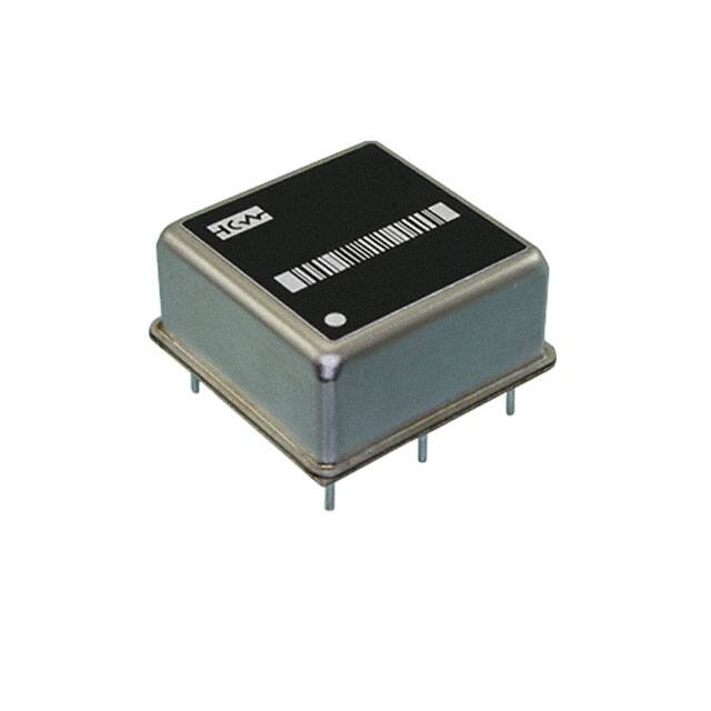
The Connor-Winfield OD100LP-series
Phone: 630- 851- 4722
is a low phase noise VCOCXO in a 1x1
• VCOCXO
• 5Vdc or 12Vdc operation
• 1x1" Metal Package
• Frequency Stability Options:
±200, ±100, ±50, ±20 and ±10ppb
• Temperature Range Options:
0 to 70°C, -40 to 85°C, -20 to 70°C
• Sinewave or HCMOS Output
• Reference Voltage Output Pin 4
• RoHS Compliant / Lead Free
2111 Comprehensive Drive
Fax: 630- 851- 5040
www.conwin.com
inch metal package. The OD100LP-series
is designed for those applications that
demand extremely low noise frequency
sources.
Pin Connections
1:
2:
3:
4:
5:
Package Outline
Output
Ground (Case)
Voltage Control
Reference Voltage
Supply Voltage (Vdd)
.500 Max.
(12.70mm)
Marking Configuration
Date Code (YYWW)
1825
Model Number
Output Frequency
Serial # Barcode
Serial Number
OD100LP-61005CV
10.0 MHz
123456789012
123456789012
Dimensional Tolerance:
±.005 (.127mm)
Ordering Information
OD100LP-
5
12
12
S
V
Package
Temperature
Range
Frequency
Stability
Supply Voltage
Output Type
OCXO Type
5 = 0 to 70°C
6 = -40 to 85°C
7 = -20 to 70°C
8 = -40 to 75°C
10 = ±10 ppb
20 = ±20 ppb
50 = ±50 ppb
12 = ±100 ppb
22 = ±200 ppb
05 = 5.0 Vdc
12 = 12.0 Vdc
S = Sinewave V = Voltage
Controlled
C = CMOS
V1 = Voltage
Control*
OD100LP- =
1.0"x1.0"x0.5"
OCXO
Through Hole
Package
- 010.0M
Output Frequency
Frequency Format
-xxx.xM Min
-xxx.xxxxxxM Max
*Max 6 digits after
the decimal point.
M = MHz
Note: See page 2 for frequencies available at each stability level. Not all combinations of supply voltage and
temperature ranges are available.
* V1 specifies 0 to +5V CV range on +12V 100MHz model
Bulletin
Page
Revision
Date
Cx292
1 of 5
08
21 July 2021
Example Part Number:
OD100LP-51212SV-010.0M = 1.0" x 1.0" x 0.445" package, 0 to 70°C temperature range, ±100 ppb frequency stability,
12V Vdc supply voltage,Sinewave output, VCOCXO, 10.0 MHz output frequency.
Attention: System Designers please review Application Note AN2093:
System Design Information and Printed Circuit Board Layout Guidelines for OCXO Oscillators.
@ www.conwin.com/technologies.html
�2111 Comprehensive Drive
Aurora, Illinois 60505
Phone: 630- 851- 4722
Fax: 630- 851- 5040
www.conwin.com
Absolute Maximum Ratings
Parameter
Storage Temperature
Supply Voltage (5V Models)
(12V Models)
Control Voltage (Vc)
Minimum
-55
-0.5
-0.5
-0.5
Nominal
-
-
-
-
Maximum
Units
Notes
Maximum
Units
Notes
Fo=100MHz
Sinewave Output
Units
Notes
125
7.0
12.6
9.0
°C
Vdc
Vdc
Vdc
Operating Specifications
Parameter
Minimum
Nominal
Parameter
Fo=10MHz
Center Frequency: (Fo)
-
10 and 100
-
MHz
Frequency Calibration
Fo=10 MHz
-200
-
200
ppb
1
Fo=100 MHz
-800
-
800
ppb
1
Frequency Stability vs Temperature
2
Stability Code 10:
-10
-
10
ppb
10MHz only
Stability Code 20:
-20
-
20
ppb
10MHz only
Stability Code 50:
-50
-
50
ppb
10MHz only
Stability Code 12:
-100
-
100
ppb 10MHz & 100MHz
Stability Code 22:
-200
-
200
ppb 10MHz & 100MHz
vs. Supply Voltage Change
Fo = 10MHz:
-0.3
-
0.3
ppb
Vcc ±5%
Fo = 100MHz
-10
-
10
ppb
Vcc ±5%
vs. Load Change
Fo = 10MHz:
-0.3
-
0.3
ppb
Load ±5%
Fo = 100MHz
-10
-
10
ppb
Load ±5%
vs. Aging per day
Fo = 10MHz
-0.5
-
0.5
ppb
3
Fo = 100MHz
-10
-
10
ppb
3
vs. Aging 1st Year
Fo = 10MHz
-50
-
50
ppb
Fo = 100MHz
-500
-
500
ppb
Operating Temperature Range:
Temperature Code 5:
0
-
70
°C
Temperature Code 6:
-40
-
85
°C
4
Temperature Code 7:
-20
-
70
°C
Temperature Code 8:
-40
-
75
°C
Warm-up Time at 25°C
-
-
2
Minutes
5
Short Term Stability (ADEV at 1s)
Fo = 10MHz
-
1.0E-11
-
6
Fo = 100MHz
-
2.0E-11
-
6
Typical Phase Noise
@1Hz offset
@ 10Hz offset
@ 100Hz offset
@ 1KHz offset
@ 10KHz offset
@ 100KHz offset
CMOS Output
-95
-125
-145
-160
-165
-165
-65
-95
-125
-155
-165
-170
dBc/Hz
dBc/Hz
dBc/Hz
dBc/Hz
dBc/Hz
dBc/Hz
Bulletin
Page
Revision
Date
Specifications subject to change without notification. See Connor-Winfield's website for latest revision.
© Copyright 2021 The Connor-Winfield Corporation Not intended for life support applications.
Cx292
2 of 5
08
21 July 2021
�2111 Comprehensive Drive
Aurora, Illinois 60505
Phone: 630- 851- 4722
Fax: 630- 851- 5040
www.conwin.com
Supply Voltage (Vdd)
Parameter
Minimum
Parameter
Minimum
Nominal
Maximum
Units
Notes
Maximum
Units
Notes
Units
Notes
Supply Voltage:
Option 05:
4.75
5.00
5.25
Vdc
Option 12:
11.4
12.0
12.6
Vdc
Supply Current (Idd)
Turn On (Vdd=5V)
-
700
-
mA
Turn On (Vdd=12V)
-
300
-
mA
Steady State at 25C (Vdd=5V)
-
220
-
mA
Steady State at 25C (Vdd=12V)
-
100
-
mA
Reference Voltage
Reference Voltage (Vdd=5V)
Reference Voltage (Vdd=12V, Fo=10.0MHz)
Reference Voltage (Vdd=12V, Fo=100.0MHz)
3.8
3.8
8.5
Nominal
4.0
4.0
9.0
4.2
4.2
9.5
Vdc
Vdc
Vdc
Input Characteristics - Voltage Control (Vc)
Parameter
Minimum
Tuning Range (Fo=10MHz)
±0.5
Tuning Range (Fo=100MHz)
±1.5
Linearity
-
Control Voltage Range Vdd=5V
0.0
Vdd=12V, (Fo=10.0M):
0.5
Vdd=12V, (Fo=100.0M): Standard
0.5
Vdd=12V, (Fo=100.0M): Option V1
0.0
Tuning Slope
Input Impedance
100K
Nominal
Maximum
-
±1.5
±3.0
±4.5
-
20
2.0
4.0
2.5
4.5
4.5
8.5
2.5
5.0
Positive
-
-
ppm
ppm
%
Vdc
Vdc
Vdc
Vdc
Ohms
CMOS Output Characteristics (Output Code C)
Parameter
Load
Output Voltage:
5.0 Vdc High (Voh)
Low (Vol)
Duty Cycle at 50% of Vcc
Rise / Fall Time: 10% to 90%
Minimum
Nominal
Maximum
Units
4.7
-
45
-
-
-
50
-
-
0.4
55
6
V
-
15
-
pF
Notes
%
ns
Sinewave Output Characteristics (Output Code S)
Parameter
Load
Output Power
Harmonics
Spurious
Minimum
-
7
-
-
Nominal
50
9
-
-
Maximum
-
11
-30
-80
Units
Ohms
dBm
dBc
dBc
Notes
Package Characteristics
OD100LP-Series Package
Hermetically sealed, resistive welded package with grounded case.
Environmental Characteristics
Shock
500 G’s 1ms, Halfsine, 3 shocks per direction, per MIL-STD 202F, Method 213B Test Condition D.
Sinusoidal Vibration 0.06” D.A. or 10G’s Peak, 10 to 500 Hz, per MIL-STD-202F, Method 204D, Test Condition A.
Random Vibration
5.35 G’s rms. 20 to 2000 Hz per MIL-STD-202F, Method 214,Test Condition 1A, 15 minutes each axis.
Moisture
10 cycles, 95% RH, Per MIL-STD-202F, Method 112.
Marking Permanency
Per MIL-STD-202F, Method 215J.
Attachment Method PCB
Through Hole Mounted
Resistance to Solder Heat
Per MIL-STD-202F, Method 210, Condition E.
Solder Process RoHS compliant, lead free. See solder profile.
Notes:
1. At time of shipment after 60 minutes of operation, @25°C.
2. Frequency stability vs. change in temperature [±(Fmax-Fmin)/(2*Fo)].
3. At time of shipment after 48 hours of operation.
4. The 100MHz frequency at 12V supply voltage is not available with temperature range -40 to 85C
5. Measured at 25°C, after 2 minutes will be within ±200ppb of the reference frequency measured 1 hour after turn-on.
6. The part is shielded from airflow during this measurement.
Specifications subject to change without notification. See Connor-Winfield's website for latest revision.
© Copyright 2021 The Connor-Winfield Corporation Not intended for life support applications.
Bulletin
Page
Revision
Date
Cx292
3 of 5
08
21 July 2021
�2111 Comprehensive Drive
Aurora, Illinois 60505
Phone: 630- 851- 4722
Fax: 630- 851- 5040
www.conwin.com
Typical Phase Noise Fo=10MHz CMOS Output
Short Term Stability (ADEV) Fo = 10MHz
Bulletin
Page
Revision
Date
Specifications subject to change without notification. See Connor-Winfield's website for latest revision.
© Copyright 2021 The Connor-Winfield Corporation Not intended for life support applications.
Cx292
4 of 5
08
21 July 2021
�2111 Comprehensive Drive
Aurora, Illinois 60505
Phone: 630- 851- 4722
Fax: 630- 851- 5040
www.conwin.com
Solder Profile
Temperature
260°C
260°C
220°C
180°C
150°C
120°C
0
10 s
Up to 120 s
60 to 90 s
Typical
Typical
Meets IPC/JEDEC J-STD-020C
Test Circuit
A
PROBE
Voltage
Control
POWER
SUPPLY
Vdd
V
10 uF
to
100 uF
3
4
2
0.01 uF
1
FREQ
COUNTER
Reference
Voltage
*
5
GROUND
*
SCOPE
15 pF for CMOS Load
50 Ohms for Sinewave Load
Revision History
Revision
Date
00
08/30/17
01
09/13/17
02
09/14/17
03
07/03/18
04
12/18/18
05
02/06/19
06
04/30/20
07
01/21/21
08
07/21/21
Description
New issue
Added 10MHz phase noise and ADEV data.
Updated Operating Specifications
Expanded frequency stability table and updated supply current.
Updated calibration specifications, reference voltages, and control voltage ranges.
Updated Tuning Ranges
Added Input Impedance specification
Updated Voltage Control - adding V1 option
Updated Voltage Control adding "Standard" and Changed Vref on 12V 10MHz
part from 5V to 4Vdc
Bulletin
Page
Revision
Date
Specifications subject to change without notification. See Connor-Winfield's website for latest revision.
© Copyright 2021 The Connor-Winfield Corporation Not intended for life support applications.
Cx292
5 of 5
08
21 July 2021
�
OD100LP-61205CV-100.0M 价格&库存
很抱歉,暂时无法提供与“OD100LP-61205CV-100.0M”相匹配的价格&库存,您可以联系我们找货
免费人工找货