Available at Digi-Key
www.digikey.com
OX200-DKV
VCOCXO
CO-8 Package
Features:
Description:
2111 Comprehensive Drive
Aurora, Illinois 60505
Phone: 630- 851- 4722
Fax: 630- 851- 5040
www.conwin.com
US Headquarters:
630-851-4722
European Headquarters:
+353-61-472221
• VCOCXO
• 12 Vdc Operation
• CO-8 Footprint
• Frequency Stability: ±5.0 ppb
• Temperature Range: -20 to 70°C
• LVCMOS Output
• Voltage Control Frequency Adjust
• RoHS Compliant / Lead Free
Connor-Winfield model OX200-DKV
is a 12 Vdc, Voltage Controlled Oven
Compensated Crystal Oscillator
(VCOCXO) in a CO-8 package. The
OX200-DKV is designed for use with
applications that require a LVCMOS
output, very high frequency stability,
low jitter and low phase noise.
Absolute Maximum Ratings
Parameter
Minimum
Nominal
Maximum
Units
Notes
-55
-55
-
-
-
-
-
-
125
85
15
50
°C
°C
Vdc
pF
CMOS Signal
Notes
Storage Temperature
Operable Temperature Range:
Supply Voltage (Vcc)
Output Load
Frequency Stabilities
Parameter
Minimum
Center Frequency: (Fo)
Frequency Calibration
Frequency Stability
vs Temperature
vs. Supply Voltage Change
vs. Load Change
vs. Aging per day
vs. Aging 5 Years
Total Tolerance
Operating Temperature Range:
Warm-up Time at 25°C
Maximum
Units
-
-100
Nominal
10.0
-
-
100
MHz
ppb
-5.0
-1.0
-1.0
-1.0
-60
-200
-20
-
-
-
-
-
-
-
-
-
5.0
1.0
1.0
1.0
60
200
70
5
1
ppb
2
ppb
Vcc ±5%
ppb
Load ±5%
ppb 30 days operation
ppb 72 hrs. operation
ppb
3
°C
Minutes
4
Supply Voltage (Vcc)
Parameter
Minimum
Nominal
Maximum
Units
Notes
Supply Voltage: (Vcc)
11.4
12.0
12.6
Vdc
Power Consumption:
Turn On
-
-
9
W
Warm up Steady State
-
-
3
W @ 25°C
Input Characteristics - Voltage Control (Vc)
Parameter
Minimum
Nominal
Maximum
Tuning Range
±0.2
-
-
Tuning Sensitivity
0.1
0.3
Linearity
-
-
20
Control Voltage Range
0.0
2.5
4.0
Tuning Slope
Positive
Units
Notes
Units
Notes
ppm
ppm/V
%
Vdc
LVCMOS Output Characteristics
Parameter
Bulletin
Page
Revision
Date
Cx286
1 of 2
00
09 March 2017
Minimum
Load -
Voltage: High (Voh)
Low (Vol)
Duty Cycle (Voh-Vol/2)
SSB Phase Noise at 1Hz offset
SSB Phase Noise at 10Hz offset
SSB Phase Noise at 100Hz offset
SSB Phase Noise at 1KHz offset
SSB Phase Noise at 10KHz offset
-
3.0
-
45
-
-
-
-
-
Nominal
-
-
-
50
-
-
-
-
-
Maximum
15
3.6
0.2
55
-90
-115
-135
-140
-140
pF
Vdc
%
dBc/Hz
dBc/Hz
dBc/Hz
dBc/Hz
dBc/Hz
�2111 Comprehensive Drive
Aurora, Illinois 60505
Phone: 630- 851- 4722
Fax: 630- 851- 5040
www.conwin.com
Pin Connections
Package Characteristics
Package
Pin Connection
1: Voltage Control (Vc)
2: N/C
3: Supply Voltage (Vcc)
4: RF Output
5: Ground (Case)
CO-8 footprint, resistive welded package with grounded case.
Environmental Characteristics
Shock
Sinusoidal Vibration
Random Vibration
Moisture
Marking Permanency
Attachment Method PCB
Resistance to Solder Heat
Solder Process
500 G’s 1ms, Halfsine, 3 shocks per direction, per MIL-
STD 202F, Method 213B Test Condition D.
0
.06” D.A. or 10G’s Peak, 10 to 500 Hz, per MIL-STD-
202F, Method 204D, Test Condition A.
5.35 G’s rms. 20 to 2000 Hz per MIL-STD-202F, Method
214,Test Condition 1A, 15 minutes each axis.
10 cycles, 95% RH, Per MIL-STD-202F, Method 112.
Per MIL-STD-202F, Method 215J.
Through Hole Mounted
Per MIL-STD-202F, Method 210, Condition E.
RoHS compliant, lead free. See solder profile.
Solder Profile
Temperature
260°C
260°C
220°C
180°C
150°C
120°C
0
Notes:
1. At time of shipment after 60 minutes of operation, @25°C, Vc = 2.5 Vdc.
2. Frequency stability vs. change in temperature [±(Fmax-Fmin)/(2*Fo)].
3. 5 years from time of shipment after 72 hours of operation and Vc = 2.5 Vdc.
4. Measured at 25°C, after 5 minutes will be within +/-100ppb of reference
frequency measured 1 hour after turn-on.
10 s
Up to 120 s
60 to 90 s
Typical
Typical
Meets IPC/JEDEC J-STD-020C
Test Circuit
Package Outline
0.530
Max.
13.46mm
0.035 Dia.
0.88mm Dia.
0.197
5.0mm Max.
Vcc Output
12 Vdc
.01 uF
1.417
36mm
0.600
15.24mm
Vc
15 pF
Ground
1
5
0.700
17.78mm
N/C
Bottom View
4
2
1.063
0.350 27mm
8.9mm
3
0.700
17.78mm
1.000
25.4mm
Marking Diagram
Ordering Information
OX200-DKV - 010.0M
1710
OX200-DKV
10.0 MHz
123456789012
123456789012
Date Code (YYWW)
Model Number
Output Frequency
Serial # Barcode
Serial Number
OCXO
SERIES
CENTER
FREQUENCY
Pin 1
Revision History
Revision
00
Date
03/09/17
Description
New issue
Bulletin
Page
Revision
Date
Specifications subject to change without notification. See Connor-Winfield's website for latest revision.
© Copyright 2017 The Connor-Winfield Corporation Not intended for life support applications.
Cx286
2 of 2
00
09 March 2017
�
很抱歉,暂时无法提供与“OX200-DKV-010.0M”相匹配的价格&库存,您可以联系我们找货
免费人工找货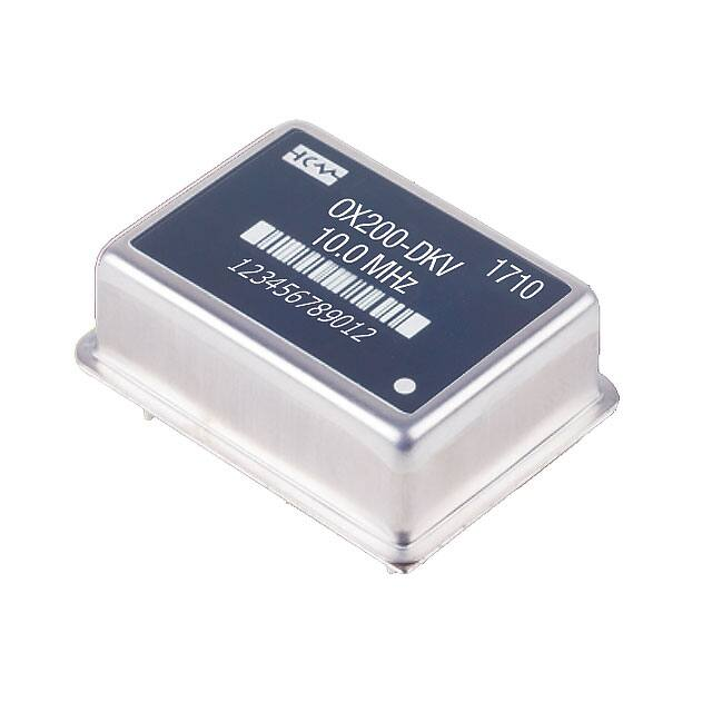


 工商网监
湘ICP备2023018690号
工商网监
湘ICP备2023018690号