物料型号:SCG4500系列
器件简介:SCG4500系列是一个混合信号相位锁定环,可从内部低抖动的电压控制晶体振荡器生成LVPECL输出,且LVPECL输出可被禁用。
引脚分配:文档中提供了详细的引脚描述表,包括引脚编号、名称和功能说明。
参数特性:
- 工作电源电压:3.3V直流
- 电源电流:在3.3V供电时,典型值为230mA
- 工作温度范围:0℃至70℃
- 自由运行频率稳定性:±20ppm
- 输入抖动容忍度:对于8kHz参考,典型值为31.25秒;对于19.44MHz参考,典型值为1微秒
功能详解:
- 双输入参考选择
- 快速锁定时间约1.5秒
- 不同参考占空比的容忍性
- 正常操作偏差的报警输出
- 丢失参考A或B时自动进入自由运行模式
- 手动进入自由运行模式
应用信息:文档中未明确列出应用信息,但从功能描述来看,该器件适用于需要精确时钟同步的通信系统。
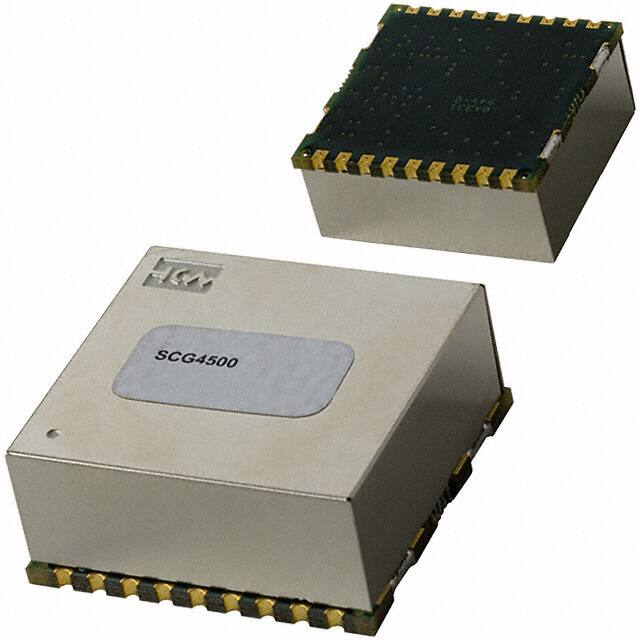
封装信息:封装尺寸为1平方英寸,采用6层FR4板,带有开槽引脚。组件使用高温焊料组装,以承受63/37合金的180°C表面贴装回流过程。