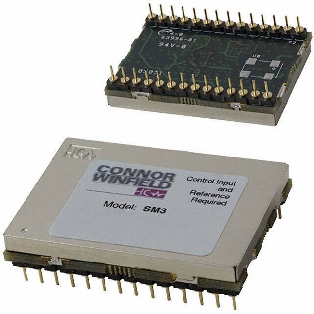
SM3
ULTRA MINIATURE
STRATUM 3 MODULE
2111 Comprehensive Drive
Aurora, Illinois 60505
Phone: 630- 851- 4722
Fax: 630- 851- 5040
www.conwin.com
Application
Bulletin
Page
Revision
Date
Issued By
TM052
1 of 36
06
26 Jan 2011
ENG
The SM3 Timing Module is a
complete system clock module for
Stratum 3 timing applications and
conforms to GR-1244-CORE
(Issue 2), GR-253-CORE (Issue
3), ITU-T G.812 (Type 3) and ITUT G813
(Option 2). Applications
include shared port adapters, data
digital cross connects, ADM’s,
DSLAM’s, multiservice platforms,
switches and routers in TDM,
SDH and SONET environments.
The SM3 Timing Module helps
reduce the cost of your design by
minimizing your development time
and maximizing your control of the
system clock with our simplified
design.
This product is compliant with all
required ROHS specifications.
Features
Small Package Size, 1.45” x 1.0”
x 0.25"
Four Auto Select Input
References, 8 kHz - 77.76 MHz
Frequency Qualification and Loss
of Reference detection for each
input
Hitless Reference Switching
Master/Slave Operation with
Phase Adjustment
Manual/Autonomous Operation
Bi-Directional SPI Port Control
Three CMOS Frequency Outputs
- Output 1 from 12.96 - 77.76
MHz, M/S Output @ 8kHz, BITS
@2.048 MHz or 1.544 MHz
3.3V operation
ROHS Compliant
�General Description
The SM3 timing module provides a clock output that meets or exceeds Stratum 3 specifications given in GR-1244-CORE (Issue 2),
GR-253-CORE (Issue 3), ITU-T G.812 (Type 3) and ITU-T G813 (Option 2). The SM3 features four reference inputs that will autodetect the following reference frequencies: 8 kHz, 1.544 MHz, 2.048 MHz, 12.96 MHz, 19.44 MHz, 25.92 MHz, 38.88 MHz, 51.84 MHz
and 77.76 MHz.
The SM3 timing module can be configured during production to produce an output up to 77.76 MHz. This output is derived from
an onboard VCXO and must be specified when ordering. The BITS output selectable for either 1.544 or 2.048 MHz. The master/slave
output is 8KHz. The user communicates with the SM3 module through a SPI port. The user controls the SM3 operation by writing to
the appropriate registers . The user can also enable or disable SPI operation through a SPI_Enable pin. The SM3 offers a wide range
of options for the system designer. The bandwidth is SPI Por t-selectable from 0.025 Hz to 1.6 Hz. 0.098 Hz is the recommended
operational bandwidth for SONET Minimum Clock and most Stratum 3 applications. The 8 kHz output has an adjustable pulse width.
The pull-in range is also adjustable to establish the desired reference frequency rejection limits. A Free Run frequency calibration
value can be written to the module to provide a high degree of accuracy in the free run mode. The reference frequency for any given
reference input is automatically detected. A wealth of status information is available through the SPI Port registers. The user also has a
choice between autonomous or full manual control operation.
In manual mode, the user controls the module operating modes Free Run, Hold Over or locked to a specific reference in normal
mode. If the chosen reference is unavailable or disqualified the module automatically enters Hold Over.
In autonomous control mode, operational mode selection occurs automatically based on reference priority and qualification status.
When the active reference becomes disqualified, the module will switch to another qualified reference. If none is available, it will switch
to Holdover. In the revertive mode the module will seek to acquire the highest priority qualified reference. In the non-revertive mode the
module will not return to the previous reference even after it is re-qualified unless there are no other qualified references.
Switching between references is hitless. Likewise, the output frequency slew rate is minimized during any change of operating
mode, including entry into and return from Free Run or Hold Over to protect traffic from transient-induced bit errors.
Reference Status information and the operating mode information is accessed through status registers. The module will set the
Interrupt pin (SPI_INT) low to indicate a status change. An Alarm pin is used to indicate failure of the active reference status.
Free Run operation guarantees an output within 4.6ppm of nominal frequency and Holdover operation guarantees the output
frequency will not change by more than 0.37ppm during the first 24 hours. Frequency accuracy is based on a TCXO for its small
size, low power consumption and outstanding performance over all environmental conditions.
The module operates on 3.3V ± 5% with a typical power draw of less than 500 milliwatts. The module operates over the 0° to 70°C
commercial temperature range.
Functional Block Diagram
Figure 1
TRST
TCK
TDO
EEPROM
OCXO
DAC
VCXO
BITS_CLK
TMS
Reference Input Monitor
M/S REF
REF 1 - 4
RESET
MASTER SELECT
4
Control
Mode
Reference
Selection
DPLL
APLL
LOS
T1/E1
SPI_ENBL
SPI_CLK
OUTPUT1
M/S_OUT
TDI
Reference Priority,
Revertivity and Mask
Table
LOL
HOLD_GOOD
SPI_IN
SPI_OUT
Bus Interface
SPI_INT
SM3 Data Sheet #: TM052
Page 2 of 36
Rev: 06
Date:01/26/11
© Copyright 2011 The Connor-Winfield Corp. All Rights Reserved Specifications subject to change without notice
�Specifications for Ultra Miniature Stratum 3
Table 1
Parameter
Voltage
Power
Operating Temp Range
Reference Frequency 1, 2, 3, 4
CMOS Output Frequency #1
M/S Output
BITS_Clk
Master/Slave Input Reference
Input Reference Pulse Width
Reference Qualification Time
Input Capacitance (LVCMOS)
Output Drive Levels (LVCMOS)
Free Run Accuracy
Hold Over Accuracy
Dimensions
Specification
3.3V ± 5%
< 500 mW
0° - 70°C
8 kHz - 77.76 MHz (Auto Detected)
12.96 MHz - 77.76 MHz
8 kHz
1.544/2.048 MHz (Selectable)
8 kHz - 77.76 MHz
10 ns Min @ 8 kHz, 5 ns Min @ >8 kHz
10 sec.
10 pF
Source Current: 7 mA, Sink Current: 10 mA
4.6 ppm
0.37 ppm
1.45 x 1.0 x 0.25 inches (36.83 x 25.4 x 6.35 mm)
Pin Description
Table 2
Pin #
1
2
3
4
5
6
7
8
9
10
11
12
13
14
15
16
17
18
19
20
21
22
23
24
25
26
27
28
I/O
Pin Name
O
O
I
I
I
I
I
O
O
O
I
I
I
O
I
I
I
I
O
O
I
LOS
LOL
M/S Ref
REF1
REF2
REF3
REF4
TDI
TMS
TRST
BITS_CLK
M/S_OUT
OUTPUT1
VPP
VPN
T1/E1
HOLD_GOOD
TDO
TCK
GND
SPI_CLK
SPI_IN
VCC
SPI_ENBL
RESET
SPI_OUT
SPI_INT
MASTER SELECT
Pin Description
Alarm Output - Loss of Active Reference Signal
Alarm Output - Loss of Lock
Master/Slave reference input – 8 kHz to 77.76 MHz auto detected
Reference Input 1 – 8 kHz to 77.76 MHz auto detected
Reference Input 2 – 8 kHz to 77.76 MHz auto detected
Reference Input 3 – 8 kHz to 77.76 MHz auto detected
Reference Input 4 – 8 kHz to 77.76 MHz auto detected
JTAG TDI pin
JTAG TMS pin
JTAG TRST pin
1.544 or 2.048 MHz output selected by pin 14
Master/Slave 8 kHz output
Synchronous Primary Output
Positive Programing Supply Pin. During normal operation, it is
recommended to float this pin.
Negative Programming Supply Pin. During normal operation it is
recommended to float this pin.
BITS_CLK select input – 1.544 MHz, 0=2.048 MHz, 4.7k Ohm Pull-up
Holdover Good Output Flag – 1=Holdover Available
JTAG TDO pin
JTAG TCK pin
Module Ground
SPI Port Clock input
SPI Port Data input
3.3 Vdc VCC Supply Input
SPI Port Enable input – Active Low, 4.7k Ohm Pull-up
Module Reset – Active Low, 10 ms Hold time
SPI Port Data Output
SPI Port Interrupt Output – Active low
Master/Slave select input – 1=Master, 0=Slave
SM3 Data Sheet #: TM052
Page 3 of 36
Rev: 06
Date: 01/26/11
© Copyright 2011 The Connor-Winfield Corp. All Rights Reserved Specifications subject to change without notice
�Pin Diagram
Figure 2
LOS
1
LOL
SM3
28
MASTER SELECT
2
27
SPI_INT
M/S REF
3
26
SPI_OUT
REF1
4
25
RESET
REF2
5
24
SPI_ENBL
REF3
6
23
Vcc
REF4
7
22
SPI_IN
TDI
8
21
SPI_CLK
TMS
9
20
GND
TRST
10
19
TCK
BITS_CLK
11
18
TDO
M/S_OUT
12
17
HOLD_GOOD
OUTPUT1
13
16
T1/E1
VPP
14
15
VPN
(TOP VIEW)
SM3 Data Sheet #: TM052
Page 4 of 36
Rev: 06
Date:01/26/11
© Copyright 2011 The Connor-Winfield Corp. All Rights Reserved Specifications subject to change without notice
�Register Map Continued
Register Map
Table 3
Address
Reg Name
0x00
0x01
0x02
0x03
0x04
0x05
0x06
0x07
0x08
0x09
0x0a
0x0b
0x0c
0x0d
0x0e
0x0f
0x10
0x11
0x12
0x13
0x14
0x15
0x16
0x17
0x18
0x19
0x1a
0x1b
0x1c
0x1d
0x1e
0x1f
0x20
0x21
0x22
0x23
0x24
0x25
0x26
0x27
0x30
0x31
0x32
0x33
0x36
0x37
0x38
0x39
Chip_ID_Low
Chip_ID_High
Chip_Revision
Bandwidth
Ctl_Mode
Op_Mode
Max_Pullin_Range
M/S REF_Activity
Ref_Activity
Ref_Pullin_Sts
Ref_Qualified
Ref_Mask
Ref_Available
Ref_Rev_Delay
Phase_Offset
Calibration
Fr_Pulse_Width
DPLL_Status
Intr_Event
Intr_Enable
Ref1_Frq_Offset1
Ref2_Frq_Offset2
Ref3_Frq_Offset3
Ref4_Frq_Offset4
Reserved
Reserved
Reserved
Reserved
Ref1_Frq_Priority1
Ref2_Frq_Priority2
Ref3_Frq_Priority3
Ref4_Frq_Priority4
Reserved
Reserved
Reserved
Reserved
FreeRun Priority
History_Policy
History_CMD
HoldOver_Time
Cfgdata
Cfgctr_Lo
Cfgctr_Hi
Chksum
EE_Wrt_Mode
EE_Cmd
EE_Page_Num
EE_FIFO_Port
Description
Type
Low byte of chip ID
High byte of chip ID
Chip revision number
Bandwidth Select
Manual or automatic selection of Op_Mode,BITS clock output frequency
indication, and frame/multi-frame sync pulse width mode control
Master Free Run, Locked, or Hold Over mode, or Slave mode
Maximum pull-in range in 0.1 ppm units
Cross Reference activity
Activities of 4 reference inputs
In or out of pull-in range of 4 reference inputs
Qualification status of 4 reference inputs
Availability mask for 4 reference inputs
Availability of 4 reference inputs
Reference reversion delay time, 0 - 255 minutes
Phase offset between M/S REF & M/S Output (for the Slave in M/S operation)
in 250ps resolution
Local oscillator digital calibration in 0.05 ppm resolution
Frame sync pulse width
Digital Phase Locked Loop status
Interrupt events
Enable individual interrupt events
Ref1 frequency offset in 0.2 ppm resolution
Ref2 frequency offset in 0.2 ppm resolution
Ref3 frequency offset in 0.2 ppm resolution
Ref4 frequency offset in 0.2 ppm resolution
Ref1 frequency and priority
Ref2 frequency and priority
Ref3 frequency and priority
Ref4 frequency and priority
Control and Priority for designation of Free Run as a reference
Sets policy for Hold Over history accumulation
Save, restore and flush comands for Hold Over history
Indicates the time since entering Hold Over state
Configuration data write register
Configuration data write counter, low byte
Configuration data write counter, high byte
Configuration data checksum pass/fail indicator
Disables/Enables writing to the external EEPROM
Read/Write command & ready indication register for ext. EEPROM access
Page number for external EEPROM access
Read/Write data for external EEPROM access
R
R
R
R/W
R/W
SM3 Data Sheet #: TM052
Page 5 of 36
Rev: 06
R/W
R/W
R
R
R
R
R/W
R
R/W
R/W
R/W
R/W
R
R
R/W
R
R
R
R
R/W
R/W
R/W
R/W
R/W
R/W
R/W
R
R/W
R
R
R
R/W
R/W
R/W
R/W
Date: 01/26/11
© Copyright 2011 The Connor-Winfield Corp. All Rights Reserved Specifications subject to change without notice
�Detailed Description
The SM3 can accept up to 4 external references from 8 kHz to 77.76 MHz and each is monitored for signal presence and
frequency offset. Additionally, a cross-couple reference input is provided for master/slave operation. Reference selection may be
manual or automatic, according to pre-programmed priorities. All reference switches are performed in a hitless manner, and frequency
ramp controls ensure smooth output signal transitions. When references are switched, the device provides an automatic phase buildout to minimize phase transitions in the output clocks.
Three output signals are provided, the first up to 77.76 MHz , the second fixed at 8 kHz for use as a Frame Sync signal as well as a
cross-couple reference for master/slave operation. The third output is a BITS clock, selectable as either 1.544 MHz or 2.048 MHz.
Device operation may be in Free Run, locked, or Hold Over modes. In Free Run, the clock frequencies are simply determined by
the accuracy of the calibrated internal clock. In locked mode, the SM3 phase locks to the selected input reference. While locked, a
frequency history is accumulated. In Hold Over mode, the output frequencies are generated according to this history.
The Digital Phase Locked Loop provides the critical filtering and frequency/phase control that meet or exceed all requirements in
critical jitter and accuracy performance parameters. Filter bandwidth may be configured to suit applications requirements.
Control functions are provided via standard SPI bus register interface. Register access provides visibility into a variety of registered
information as well as providing extensive programmable control capability.
Operating Modes: The SM3 Operates in Either Free Run, Locked, or Hold Over Mode:
Free Run – In Free Run mode, Output 1, M/S Output, and BITS_Clk, the output clocks, are determined directly from and
have the accuracy of the calibrated free running internal clock. Reference inputs continue to be monitored for signal presence and
frequency offset, but are not used to synchronize the outputs.
Locked – The Output 1, M/S Output, and BITS_Clk, outputs are phase locked and track the selected input reference. Upon
entering the Locked mode, the device begins an acquisition process that includes reference qualification and frequency slew rate
limiting, if needed. Once satisfactory lock is achieved, the “Locked” bit is set in the DPLL_Status register, and a compilation of the
frequency history of the selected reference is started. When a usable Hold Over history has been established, the Hold_Good pin is
set, and the “Hold Over Available” bit is set in the DPLL_Status register.
Phase comparison and phase lock loop filtering operations in the SM3 are completely digital. As a result, device and loop behavior
are entirely predictable, repeatable, and extremely accurate. Carefully designed and proven algorithms and techniques ensure
completely hit-less reference switches, operational mode changes, and master/slave switches.
Basic loop bandwidth is programmable from .025 Hz to 1.6 Hz, giving the user a wide range of control over the system response.
When a new reference is acquired, maximum frequency slew limits ensure smooth frequency changes. Once lock is achieved,
( 10 seconds and is within the pull-in range, it’s bit is
set.
The Ref_Available register contains the “anded” condition of the Ref_Qualified register and the Ref_Mask register, and therefore
represents the availability of a reference for selection when automatic reference and operational mode selection is enabled.
Reference Input Selection, Frequencies, and Mode Selection
One of four reference input signals (Ref 1-4) are selected for synchronization in Master mode (as below in the Op_Mode register
description. 0x05). Ref1-4 may each be 8 kHz, 1.544 MHz, 2.048 MHz, 12.96 MHz, 19.44 MHz, 25.92 MHz, 38.88 MHz, 51.84 MHz
or 77.76 MHz.
Reference frequencies are auto-detected (frequency determined by the chip) and the detected frequency can be read from the
Ref_Frq_Priority registers (See Register Descriptions and Operation section).
The M/S REF input for slave operation is frequency auto-detected and may be 8kHz, 1.544MHz, 2.048MHz, 12.96MHz, 19.44MHz,
25.92MHz, 38.88MHz, 51.84MHz or 77.76MHz. Signal presence and frequency for the M/S REF input is indicated in bits 0-3 of the
M/S REF_Activity register.
Active reference and operational mode selection may be manual or automatic, as determined by bit 1 in the Ctl_Mode register. In
manual mode, register writes to Op_Mode select the reference and mode. The reset default is manual mode.
In automatic mode, the reference is selected according to the priorities written to the four Ref_Frq_Priority registers. Individual
references may be masked for use/non-use according to the Ref_Mask register. A reference may only be selected if it is “available”
- that is, it is qualified, as indicated in the Ref_Qualified register, and is not masked (See Reference Input Quality Monitoring and
Register Descriptions and Operation sections).
Furthermore, Bit 3 of each Ref_Frq_Priority register will determine if that reference is revertive or non-revertive. When a reference
fails, the next highest priority “available” (signal present, non-masked, and acceptable frequency offset) reference will be selected.
When a reference returns, it will be switched to only if it is of higher priority and the current active reference is marked “Revertive”.
Additionally, the reversion is delayed according to the value written to the Ref_Rev_Delay register (From 0 to 255 minutes).
SM3 Data Sheet #: TM052
Page 9 of 36
Rev: 06
Date: 01/26/11
© Copyright 2011 The Connor-Winfield Corp. All Rights Reserved Specifications subject to change without notice
�Detailed Description continued
The automatic reference selection is shown in the following state diagram:
Automatic Reference Selection
Figure 6
Stay
Locked on Ref m
time for t=
Ref_Rev_Delay
Ref_Rev_Delay
time expired
Ref n returns,
Ref m marked
“revertive”
Select &
Lock on
Ref m
Loss of Ref n
Locked
on Ref n
Ref n returns,
Ref m marked
“non-revertive”
Select new reference:
Next highest priority,
Qualified (within max. pull-in range, signal present > 10 sec.),
Non-masked
The operational mode is according to the following state diagram:
No available reference and no Hold Over history
Ref loss w/no good Hold Over history and no other available reference
Automatic Operational Mode Selection
Figure 7
Reference Available
(Select highest priority)
Higher priority Ref return with
prior reference marked
“revertive”
Ref Loss w/alternate
reference available
Locked
Ref loss w/no good hold
over history and no other
available reference
No available
reference and
no hold over
history
Ref Loss w/good hold over history
and no alternate reference available
Ref
Return
Ref
Return
Free Run
Hold Over
SM3 Data Sheet #: TM052
Page 10 of 36
Rev: 06
Date:01/26/11
© Copyright 2011 The Connor-Winfield Corp. All Rights Reserved Specifications subject to change without notice
�Detailed Description continued
Output Signals and Frequency
Output 1 is the primary output, and in locked mode is synchronized to the selected reference. Output 1 must be specified at the
time of ordering as any one of the following frequencies : 12.96 MHz, 19.44 MHz, 25.92 MHz, 38.88 MHz, 51.84 MHz or 77.76 MHz.
M/S Output is an 8 kHz output available as a frame reference or synchronization signal for cross-coupled pairs of SM3 devices
operated in master/slave mode. In master mode, M/S Output is synchronized to the selected reference. In slave mode, M/S Output
is in phase with the M/S REF offset by the value written to the Phase_offset register (+31.75 to -32nS, with .25nS resolution). M/S
Output may be a 50% duty cycle signal, or variable high-going pulse width, as determined by the Ctl_Mode and Fr_Pulse_Width
registers. In variable pulse width mode, the width may be from 1 to 15 multiples of the Output 1 cycle time. See Register Descriptions
and Operation section.
BITS_Clk is the BITS clock output at either 1.544 MHz or 2.048 MHz. It is selected by the T1/E1 input and its state may be read in
bit 3 of the Ctl_Mode register. When T1/E1 = 1, the BITS frequency is 1.544 MHz, and when T1/E1 = 0, the BITS frequency is 2.048
MHz. This output clock is digitally synthesized from Output1 directly and will be synchronized to M/S Output.
Interrupts
The SM3 module supports eight different interrupts and appears in INTR_EVENT (0x12) register. Each interrupt can be individually
enabled or disabled via the INTR_ENABLE (0x13) register. Each bit enables or disables the corresponding interrupt from asserting
the SPI_INT pin. Interrupt events still appear in the INTR_EVENT (0x12) register independent of their enable state. All interrupts are
cleared once INTR_EVENT (0x12) register is read. The interrupts are:
•
Any reference changing from available to not available
•
Any reference changing from not available to available
•
M/S REF changing from activity to no activity
•
M/S REF changing from no activity to activity
•
DPLL Mode status change
•
Reference switch in automatic reference selection mode
•
Loss of Signal
•
Loss of Lock
Interrupts and Reference Change in Autonomous Mode
Interrupts can be used to determine the cause of a reference change in autonomous mode. Let us assume that the module is
currently locked to REF1. The module switches to REF2 and SPI_INT pin is asserted. The user reads the INTR_EVENT (0x12)
register.
If the module is operating in autonomous revertive mode, the cause can be determined from bits 1, 4,5, 6 and 7. Bit 5 is set to
indicate Active reference change. If Bit 6 is set then the cause of the reference change is Loss of Active Reference. If Bit 7 is set
then the cause of the reference change is a Loss of Lock alarm on the active reference. If Bit 1 is set then the cause of the reference
change is the availability of a higher priority reference.
Note: The DPLL Mode Status Change bit (Bit 4) is also set to indicate a change in DPLL_STATUS (0x11) register, during an
interrupt caused by a reference change. The data in DPLL_STATUS (0x11) register however is not useful in determining the cause of
a reference change. This is because bits 0-2 of this register always reflects the status of the current active reference and hence cannot
be used to determine the status of the last active reference.
Interrupts in Manual Mode
In manual operating mode, when the active reference fails due to a Loss of Signal or Loss of Lock alarm, an interrupt is generated.
For example, in case of a Loss of Signal, bits4 and 6 of INTR_EVENT (0x12) register would be set to indicate Loss of Signal and
DPLL Mode Status Change. The user may choose to read the DPLL_STATUS (0x11) register, though in manual mode bit6 of INTR_
EVENT (0x12) register is a mirror of bit0 of DPLL_STATUS (0x11) register. This holds true for a Loss of Lock alarm, where bit7 of
INTR_EVENT (0x12) register is a mirror of bit1 of DPLL_STATUS (0x11) register.
Internal Clock Calibration
The internal clock may be calibrated by writing a frequency offset v.s. nominal frequency into the Calibration register. This
calibration is used by the synchronization software to create a frequency corrected from the actual internal clock output by the value
written to the Calibration register. See register descriptions.
SM3 Data Sheet #: TM052
Page 11 of 36
Rev: 06
Date: 01/26/11
© Copyright 2011 The Connor-Winfield Corp. All Rights Reserved Specifications subject to change without notice
�Register Descriptions and Operation
Chip_ID_low, 0x00 (R)
Bit 7 ~ Bit 0
Low byte of chip ID: 0x12
Chip_ID_High, 0x01 (R)
Bit 7 ~ Bit 0
High byte of chip ID: 0x30
Chip_Revision, 0x02 (R)
Bit 7 ~ Bit 0
Chip revision number: 0x05
Bandwidth, 0x03 (R/W)
Bit 7 ~ Bit 5
Reserved
Bit 4
Reserved
0:Default
Bit 3 ~ Bit 0
Bandwidth Selection in Hz:
0000: 0.025
0001: 0.025
0010: 0.025
0011: 0.025
0100: 0.025
0101: 0.025
0110: 0.049
0111: 0.098(Reset Default)
1000: 0.20
1001: 0.39
1010: 0.78
1011 - 1111: 1.6
BITS 3 - 0 select the phase lock loop bandwidth in Hertz. The reset default is 0.098 Hz.
Ctl_Mode, 0x04 (R/W)
Bit 7 ~ Bit 6
Reserved
Bit 5
Default: 0
Bit 4
M/S Output
Pulse width
control:
0: 50%
1: Controlled by
FR_Pulse_Width
register
Default: 0
Bit 3
Bit 2
Bit 1
BITS Clock
Output
Frequency:
1: 1.544 MHz
0: 2.048 MHz
(read only)
HM Ref:
0: Register control
of op mode/ref
(Will always
be 0)
Active
Reference
Selection:
1: Manual
0: Automatic
Default: 1
Bit 0
Reserved
When bit 1 is reset (automatic reference and mode selection), Bits 3 - 0 of the Op_Mode register become read-only.
The power-up default for Bit 1 = 1 for manual reference selection and default for Bit 4 = 0 for 50% duty cycle on M/S
Output.
SM3 Data Sheet #: TM052
Page 12 of 36
Rev: 06
Date:01/26/11
© Copyright 2011 The Connor-Winfield Corp. All Rights Reserved Specifications subject to change without notice
�Register Descriptions and Operation continued
When the device is in slave mode, it will lock to the M/S REF, independent of the values written to BITS 3 - 0 of the
Op_mode register. The operational mode and reference selection written to Bits 3 - 0 while in slave mode will, however,
take effect when the device is made the master.
When bit 1 of the Ctl_Mode register is reset (automatic reference and mode selection) and the device is in master
mode, BITS 3 - 0 of the Op_Mode register become read-only.
Op_Mode, 0x05 (R/W)
Bit 7 ~ Bit 5
Reserved
Bit 4
Bit 3 ~ Bit 0
Master or Slave Mode
1: Master
0: Slave
(Read Only)
Free Run, Locked, or Hold Over:
0000: Free Run mode
0001: Locked on Ref1
0010: Locked on Ref2
0011: Locked on Ref3
0100: Locked on Ref4
0101 - 1000: Not Used
1001 - 1111: Hold Over
Max_Pullin_Range, 0x06 (R/W)
Bit 7 ~ Bit 0
Maximum pull-in range in 0.1 ppm unit
This register should be set according to the values specified by the standards (GR-1244) appropriate for the particular
stratum of operation. The power-up default value is 10 ppm. (= 4.6ppm aging + 4.6 ppm pullin + margin).
M/S_Activity, 0x07 (R)
Bit 7 ~ Bit 4
Reserved
Bit 3 ~ Bit 0
Cross reference activity
0000: No signal
0001: 8kHz
0010:1.544 MHz
0011:2.048MHz
0100: 12.96MHz
0101: 19.44MHz
0110: 25.92MHz
0111: 38.88MHz
1000: 51.84MHz
1001: 77.76MHz
1010-1111: Reserved
Indicates signal presence and auto-detected frequency for the M/S REF input.
Ref_Activity, 0x08 (R)
Bit 7
Bit 6
Bit 5
Bit 4
Bit 3
Bit 2
Bit 1
Bit 0
x: Don’t
Care
x: Don’t
Care
x: Don’t
Care
x: Don’t
Care
ref4 activity
1: on
0: off
ref3 activity
1: on
0: off
ref2 activity
1: on
0: off
ref1 activity
1: on
0: off
Each bit indicates the presence of a signal for that reference. Reference bits 4-7 are not used but may be 1 or 0.
SM3 Data Sheet #: TM052
Page 13 of 36
Rev: 06
Date: 01/26/11
© Copyright 2011 The Connor-Winfield Corp. All Rights Reserved Specifications subject to change without notice
�Register Descriptions and Operation continued
Ref_Pullin_Sts, 0x09 (R)
Bit 7
0: Default
range
Bit 6
0: Default
Bit 5
0: Default
Bit 4
Bit 3
0: Default
ref4 sts
1: in range
0: out range
Bit 2
ref3 sts
1: in range
0: out range
Bit 1 Bit 0
ref2 sts
1: in range
0: out range
ref1 sts
1: in range
0: out
Each bit indicates if the reference is within the frequency range specified by the value in the Max_Pullin register.
Ref_Qualified, 0x0a (R)
Bit 7
0: Default
Bit 6
0: Default
Bit 5
0: Default
Bit 4
0: Default
Bit 3
Bit 2
ref4 qual:
1: avail.
0: not avail.
ref3 qual:
1: avail.
0: not avail.
Bit 1 Bit 0
ref2 qual:
1: avail.
0: not avail.
ref1 qual:
1: avail.
0: not avail.
This register contains the “anded” condition of the Ref_Activity and Ref_Pullin_Sts registers for each of the Ref1-4 inputs,
qualified for 10 seconds. When a reference signal has been present for > 10 seconds and is within the pull-in range, it’s
bit is set.
Ref_Mask, 0x0b (R/W)
Bit 7
0: Default
Bit 6
0: Default
Bit 5
0: Default
Bit 4
0: Default
Bit 3
Bit 2
ref4 mask:
1: avail.
0: not avail.
Default: 0
ref3 mask:
1: avail.
0: not avail.
Default: 0
Bit 1 Bit 0
ref2 mask:
1: avail.
0: not avail.
Default: 0
ref1 mask:
1: avail.
0: not avail.
Default: 0
Individual references may be marked as “available” or “not available” for selection in the automatic reference selection
mode
(bit 1 = 0 in the Ctl_Mode register). The reset default value is 0, “not available”. In manual reference selection, either
hardware or register controlled, the reference masks have no effect, but do remain valid and are applied upon a transition to automatic mode.
Ref_Available, 0x0c (R)
Bit 7
0: Default
Bit 6
0: Default
Bit 5
0: Default
Bit 4
0: Default
Bit 3
Bit 2
ref4 avail:
1: avail.
0: not avail.
ref3 avail:
1: avail.
0: not avail.
Bit 1 Bit 0
ref2 avail:
1: avail.
0: not avail.
ref1 avail:
1: avail.
0: not
This register contains the “anded” condition of the Ref_Qualified and Ref_Mask registers.
Ref_Rev_Delay, 0x0d (R/W)
Bit 7 ~ Bit 0
Reference reversion delay time, 0 - 255 minutes. default, 0000 0101, 5 minutes
In automatic reference selection mode, when a reference fails and later returns, it must be available for the time specified in the Ref_Rev_Delay register before it can be switched back to as the active reference (if the new reference was
marked as “revertive”). See Figure 7.
SM3 Data Sheet #: TM052
Page 14 of 36
Rev: 06
Date:01/26/11
© Copyright 2011 The Connor-Winfield Corp. All Rights Reserved Specifications subject to change without notice
�Register Descriptions and Operation continued
Phase_Offset, 0x0e (R/W)
Bit 7 ~ Bit 0
The 2’s complement value of phase offset between Master Output module and Slave Output module, ranges from -32 nS to +31.75 nS
Positive Value: Master Output rising edge leads Slave Output
Negative Value: Master Output rising edge lags Slave Output
In slave mode, the slave’s outputs may be phase shifted -32nS to +31.75nS in .25nS increments, relative to the Master
module according to the contents of the Phase_Offset register, to compensate for the path length of the Master to Slave
connection.
If a phase offset is used, then the two SM3 devices would typically be written to the appropriate phase offset values for
the respective path lengths of each Master to Slave connection, to ensure that the same relative output signal phases
will persist through master/slave switches.
Calibration, 0x0f (R/W)
Bit 7 ~ Bit 0
2’s complement value of local oscillator digital calibration in 0.05 ppm resolution
To digitally calibrate the free running clock synthesized from the internal clock, this register is written with a value corresponding to the known frequency offset of the oscillator from the nominal center frequency.
Fr_Pulse_Width, 0x10 (R/W)
Bit 7 ~ Bit4
Reserved
Bit 3 ~ Bit 0
Pulse width for M/S clock output,
1-15 multiples of the Sync_Clk clock period.
BITS 4 and 5 of the Ctl_Mode register determine if the M/S 8 kHz output is 50% duty cycle or pulsed (high going) outputs. When they are pulsed, the Fr_Pulse_Width register determines the width. Width is the register value multiple of the
Sync_Clk clock period. Valid values are 1 - 15.
Reset default is 0001. Writing to 0000 maps to 0001.
DPLL_Status, 0x11 (R)
Bit 7 ~Bit 5
Reserved
Bit 4
Hold Over
Build
Complete
1: Complete
0: Incomplete
Bit 3
Hold Over
Available
1: Avail.
0: Not avail.
Bit 2
Locked
1: Locked
0: Not locked
Bit 1
Loss of Lock
1: Loss of Lock
0: No loss of lock
Bit 0
Loss of Signal
1: No activity
on active
reference
0: Active ref-
erence signal
present
Bit 0 indicates the presence of a signal on the selected reference.
Bit 1 indicates a loss of lock (LOL). Loss of lock will be asserted if lock is not achieved within the specified time for the
stratum level of operation, or lock is lost after being established previously. LOL will not be asserted for automatic reference switches.
Bit 2 indicates successful phase lock. It will typically be set in