Telecom Performance TCXO / VCTCXO
Description
2111 Comprehensive Drive Aurora, Illinois 60505 Phone: 630- 851- 4722 Fax: 630- 851- 5040 www.conwin.com
Features:
Miniature 5.0 x7.0mm Surface Mount Package 3.3V Operation LVCMOS or Clipped Sinewave Output Logic Frequency Stabilities Available: T50x / T60x: +/-0.28ppm T51x / T61x: +/-0.50ppm T52x / T62x: +/-1.00ppm Temperature Ranges Available: T5xx Series: 0 to 70°C T6xx Series: -40 to 85°C Frequency Tolerance: +/-4.60ppm for 20 yrs. Low Jitter 100KHz offset Start Up Time (Vcc) (Icc) Minimum -1.00 -0.2 -0.2 -0.4 -4.60 3.135 Nominal 3.3 6 3 0.3 -80 -110 -135 -150 -150 Maximum 1.00 0.2 0.2 0.4 4.60 3.465 10 5 1.0 -70 -100 -130 -145 -150 10 Units ppm ppm ppm ppm ppm Vdc mA ps rms ps rms dBc/Hz dBc/Hz dBc/Hz dBc/Hz dBc/Hz ms
Table 9.0 Notes 1
2 3 4
Features TCXO VCTCXO 3.3V Operation LVCMOS Output Clipped Sinewave Output Frequency Stability: T50x/T60xSeries+/-0.28ppm T51x/T61x-Series+/-0.50ppm T52x/T62x-Series+/-1.00ppm Temperature Range: T5xx-Series 0 to 70°C T6xx-Series -40 to 85°C Low Jitter 40 MHz)
Notes: 1) TCXO: Initial calibration @ 25 C. Specifications at time of shipment after 48 hours of operation. 2) Frequency change after reciprocal temperature ramped over the operating range. Frequency measured before and after at 25°C. 3) Inclusive of calibration @ 25 C, frequency vs. change in temperature, change in supply voltage (±5%), load change (±5%), reflow soldering process and 20 years aging. 4) For best in application performance, careful selection of an external power source is critical. Select an external regulator that meets or exceeds the following specifications regarding voltage regulation tolerance, initial accuracy, temperature coefficient, voltage noise, and low voltage noise density. Factory Test Conditions: Initial Accuracy ±2mv, Noise (0.1Hz to 10 KHz) 15uV p-p, Voltage Noise Density = 50nV/square root of Hz, Temperature Coefficient < 5ppm per degree C. 5) Leave Pad 8 unconnected if enable / disable function is not required. When tristated, the output stage is disabled but the oscillator and compensation circuit are still active (current consumption < 1 mA). 6) Additional pull ranges are available; please contact the factory for additional information. 7) Output is AC coupled.
Specifications subject to change without notice. All dimensions in inches. © Copyright 2008 The Connor-Winfield Corporation
Minimum 1.00 0.80
Nominal 10K 10 -
Maximum -
Units Ohms pF V pk-pk V pk-pk
Notes 7
Voltage Control Vcc Supply Voltage .01 uF Bypass E/D DNC DNC 1 10 9 8 7 6 10Kohm 10 pF 2 3 4 5 Output
US Headquarters: 630-851-4722 European Headquarters: +353-61-472221
Bulletin Page Revision Date Tx176 3 of 4 07
25 Aug 2008
�2111 Comprehensive Drive Aurora, Illinois 60505 Phone: 630-851-4722 Fax: 630-851-5040 www.conwin.com
Design Recommendations
Vcc, should have a large copper area for reduced inductance. Connect a 0.01uF bypass capacitor
很抱歉,暂时无法提供与“T602-019.44M”相匹配的价格&库存,您可以联系我们找货
免费人工找货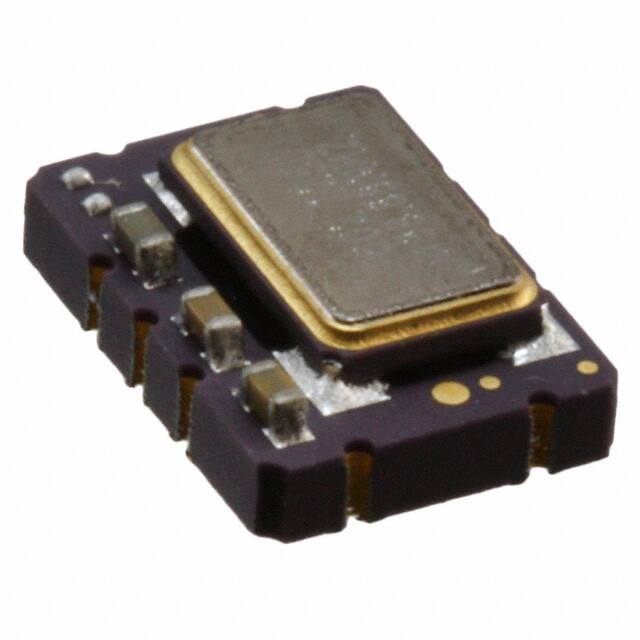


 工商网监
湘ICP备2023018690号
工商网监
湘ICP备2023018690号
