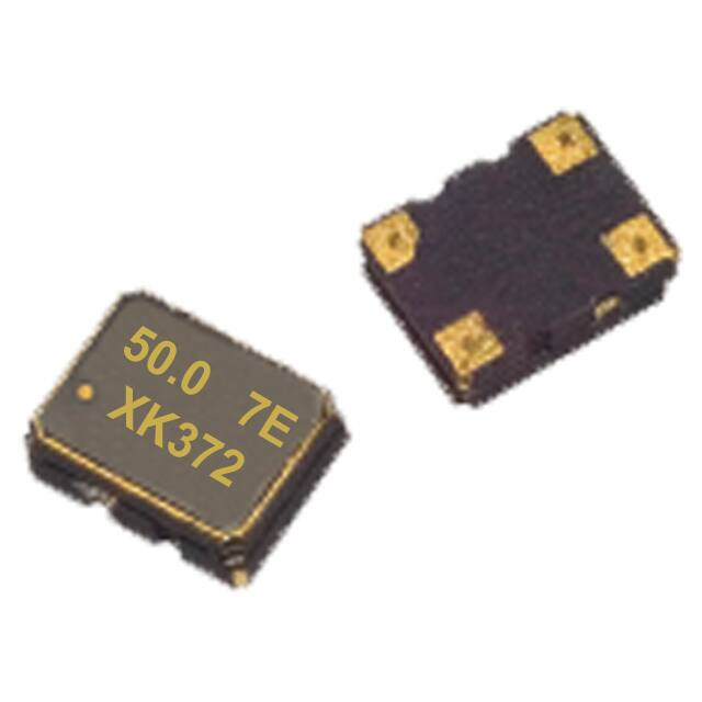
0
登录后你可以
  • 下载海量资料
  • 学习在线课程
  • 观看技术视频
  • 写文章/发帖/加入社区
会员中心
创作中心
发布
  • 发文章

  • 发资料

  • 发帖

  • 提问

  • 发视频

创作活动
XK372-020.0M

XK372-020.0M

  • 厂商:

    CONNOR-WINFIELD

  • 封装:

    SMD-4

  • 描述:

    有源晶振 20MHz 3.3V SMD-4

  • 详情介绍
  • 数据手册
  • 价格&库存
XK372-020.0M 数据手册
XK372 3.2x2.5mm LVCMOS Clock Oscillator 2111 Comprehensive Drive Aurora, Illinois 60505 Phone: 630- 851- 4722 Fax: 630- 851- 5040 www.conwin.com Description: Features: The Connor-Winfield XK372 3.2x2.5 mm, LCMOS, Surface Mount, Crystal Controlled Oscillators (XO) are designed for applications requiring low jitter and tight frequency stability. The RoHS compliant surface mount package is designed for high-density mounting and is optimum for mass production. • Supply Voltage: 3.3V Operation • Frequency Tolerance: ±50 ppm • Temperature Range: -40 to 85°C • LVCMOS Output Logic • Tri-State Enable/Disable Pad 1 • Low Jitter < 0.1ps RMS • Ceramic Surface Mount Package • Tape and Reel Packaging • RoHS Compliant / Lead Free Package Layout 0.125 (3.2mm) 4 0.051 Max. (1.3mm Max.) 3 0.055 (1.4mm) 50.0 7E XK372 1 1 0.047 (1.2mm) Suggested Pad Layout 0.098 (2.5mm) 2 Pad Connections 0.031 (0.8mm) 1: 0.055 (1.4mm) 0.020 4 (0.50mm) 3 0.047 (1.2mm) 1 2 0.047 (1.2mm) 2 2: 3: 4: Output Enable (OE) Ground Output Supply Voltage (Vdd) Top View 0.027 (0.7mm) Bottom View Dimensional Tolerance: ±0.005 (±0.127mm) 4 3 Marking drawing 90231DWG74 Ordering Information XK3 7 2 -050.0M Oscillator Type Supply Voltage and Temperature Range Frequency Stability Output Frequency 3.2x2.5 mm LVCMOS Clock Oscillator Series 7 = 3.3V, -40 to 85°C 2 = ±50 ppm Frequency Format -xxx.xM Min.* -xxx.xxxxxxM Max* *Max 6 digits after decimal point M = MHz Example Part Number: XK372-050.0M Absolute Maximum Ratings Parameter Minimum Storage Temperature Supply Voltage (Vdd) Input Voltage -0.5 Nominal -55 - -0.5 - - Maximum 125 5.0 Vdd + 0.5 Units Notes Units Notes Units Notes °C Vdc Vdc Input Characteristics Parameter Enable Input Voltage - (Vih) Disable Input Voltage - (Vil) Standby Current (Osc. Disabled) Minimum 70%Vdd - - Nominal - - - Maximum - 30%Vdd 10 Vdc 1 Vdc 1 uA LVCMOS Output Characteristics Parameter Bulletin Page Revision Date Sm145 1 of 2 01 04 Feb 2021 Load Voltage High (Voh) Low (Vol) Duty Cycle at 50% Level Rise / Fall Time: 10% to 90% Minimum - 90%Vdd - 45 - Nominal 15 - - 50 5 Maximum - - 10%Vdd 55 8 pF Vdc Vdc % ns 2111 Comprehensive Drive Aurora, Illinois 60505 Phone: 630- 851- 4722 Fax: 630- 851- 5040 www.conwin.com Operating Specifications Parameter Minimum Nominal Maximum Units Notes Output Frequency (Fo) 20 - 50 MHz Total Frequency Tolerance: -50 50 PPM 2 Operating Temperature Range: -40 85 °C Supply Voltage (Vdd) 3.135 3.465 Vdc Supply Current (Idd) 10 mA Jitter: Period Jitter - 3 5 ps RMS Integrated Phase Jitter - 60 100 fs RMS 3 SSB Phase Noise Fo = 50 MHz @ 10 Hz offset - -70 - dBc/Hz @ 100 Hz offset - -105 - dBc/Hz @ 1 KHz offset - -140 - dBc/Hz @ 10 KHz offset - -165 - dBc/Hz @ 100 KHz offset - -170 - dBc/Hz Start Up Time - 2 5 ms Notes: 1. When the oscillator is disabled the output is at high impedance. Output is enabled with no connection on pad 1. 2. Includes calibration @ 25°C, frequency stability vs. change in temperature, supply voltage and load variations, shock and vibration and 10 years aging. 3. BW = 12 KHz to Fo/2 MHz. LVCMOS Output Waveform Package Characteristics Package 90% Hermetically sealed ceramic package and metal cover 50% Enable / Disable Function Pad 1 Input: High or Open: (Voh) Low: (Vol) Output: 10% Enabled Disabled (High Impedance) Test Circuit Environmental Characteristics Vdd Vibration: Vibration per Mil Std 883E Method 2007.3 Test Condition A. Shock: Mechanical Shock per Mil Std 883E Method 2002.4 Test Condition B. Soldering Process: RoHS compliant lead free. See soldering profile below. OSCILLOSCOPE A PROBE POWER SUPPLY 3 4 V OSC .01uf 1 CL 2 FREQ COUNTER INPUT for E/D Solder Profile Tape and Reel Dimensions Temperature 260°C 260°C .488 (12.4mm) Direction of Feed (Customer) .157 (4mm) .079 (2mm) .059 (1.5mm) .069 (1.75mm) .216 (5.5mm) .315 (8mm) .059 (1.5mm) .795 (20.2mm) .059 (1.5mm) 7.09 (180mm) 2.36 (60mm) .472 (12mm) .059 (1.5mm) Meets EIAi481A and EIAJ-1009B 2000 Pieces per Reel .059 (1.5mm) 220°C 180°C 150°C 120°C 0 10 s Up to 120 s 60 to 90 s Typical Typical Meets IPC/JEDEC J-STD-020C .512 (13mm) Bulletin Page Revision Date Specifications subject to change without notification. See Connor-Winfield's website for latest revision. © Copyright 2021 The Connor-Winfield Corporation Not intended for life support applications. Sm145 2 of 2 01 04 Feb 2021
XK372-020.0M
物料型号:XK372

器件简介:该振荡器设计用于需要低抖动和紧密频率稳定性的应用。它符合RoHS标准,采用表面贴装封装,适合高密度安装和大规模生产。

引脚分配: 1. 输出使能(OE) 2. 地(GND) 3. 输出 4. 供电电压(Vdd)

参数特性: - 供电电压:3.3V - 频率容差:±50 ppm - 温度范围:-40至85°C - LVCMOS输出逻辑 - 三态使能/禁用垫 - 低抖动:<0.1ps RMS - 陶瓷表面贴装封装 - 胶带和卷轴包装 - 符合RoHS/无铅焊盘连接

功能详解: - 该振荡器具有低抖动和高频率稳定性,适用于对时钟精度要求较高的应用。 - 提供了输出使能/禁用功能,允许用户根据需要控制振荡器的输出。

应用信息: - 适用于需要低抖动和高频率稳定性的电子设备。

封装信息: - 尺寸:3.2x2.5mm - 封装类型:陶瓷表面贴装封装
XK372-020.0M 价格&库存

很抱歉,暂时无法提供与“XK372-020.0M”相匹配的价格&库存,您可以联系我们找货

免费人工找货
XK372-020.0M
  •  国内价格 香港价格
  • 100+33.74858100+4.22052

库存:73

XK372-020.0M
  •  国内价格 香港价格
  • 1+45.247431+5.65853
  • 10+39.0642010+4.88527
  • 50+35.2639150+4.41002

库存:73