rev. page page date date 1 of 3
10/2008
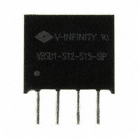
PART NUMBER: VBSD1-SIP Series
DESCRIPTION: dc-dc converter
description
Designed to convert fixed voltages into isolated voltages, the VBSD1-SIP series is well suited for providing board-mount local supplies in a wide range of applications, including mixed analog/digital circuits, test & measurement equip., process/machine controls, datacom/telecom fields, etc... The semi-regulated output can be followed by 3-terminal regulators to provide output protection, in addition to output regulation
features
·isolated 1 W output ·SIP package ·unregulated ·temperature range: -40°C~+85°C ·high efficiency to 80% ·single voltage output ·small footprint ·industry standard pinout ·UL94-V0 package ·no heatsink required ·1K Vdc isolation ·power density 0.85 W/cm ·no external component required ·low cost
MODEL
VBSD1-S3.3-S3.3-SIP VBSD1-S3.3-S5-SIP VBSD1-S5-S3.3-SIP VBSD1-S5-S5-SIP VBSD1-S5-S9-SIP VBSD1-S5-S12-SIP VBSD1-S5-S15-SIP VBSD1-S12-S3.3-SIP VBSD1-S12-S5-SIP VBSD1-S12-S9-SIP VBSD1-S12-S12-SIP VBSD1-S12-S15-SIP VBSD1-S15-S3.3-SIP VBSD1-S15-S5-SIP VBSD1-S15-S9-SIP VBSD1-S15-S12-SIP VBSD1-S15-S15-SIP VBSD1-S24-S3.3-SIP VBSD1-S24-S5-SIP VBSD1-S24-S9-SIP VBSD1-S24-S12-SIP VBSD1-S24-S15-SIP VBSD1-S24-S24-SIP
input voltage nominal range. (V dc) (V dc)
output voltage max. (V dc)
output current max. min. (mA) (mA)
efficiency (%) UL60950-1
3.3 3.3 5 5 5 5 5 12 12 12 12 12 15 15 15 15 15 24 24 24 24 24 24
3.0~3.6 3.0~3.6 4.5~5.5 4.5~5.5 4.5~5.5 4.5~5.5 4.5~5.5 10.8~13.2 10.8~13.2 10.8~13.2 10.8~13.2 10.8~13.2 13.5~16.5 13.5~16.5 13.5~16.5 13.5~16.5 13.5~16.5 21.6~26.4 21.6~26.4 21.6~26.4 21.6~26.4 21.6~26.4 21.6~26.4
3.3 5 3.3 5 9 12 15 3.3 5 9 12 15 3.3 5 9 12 15 5 5 9 12 15 24
300 200 300 200 111 83 67 300 200 111 83 67 300 200 111 83 67 300 200 111 83 67 42
30 20 30 20 12 9 7 30 20 12 9 7 30 20 12 9 7 30 20 12 9 7 4
72 73 74 78 79 80 78 75 78 80 81 79 73 74 75 79 79 76 79 80 81 79 80
NO NO NO YES YES YES YES NO YES YES YES YES NO NO NO NO NO NO YES YES YES YES NO
notes: 1. All specifications measured at TA=25°C, humidity 3,500,000 hours full load at +85°C, for 4 hours at no-load and 4 hours at full load.
ISOLATION SPECIFICATIONS
parameter isolation voltage isolation resistance conditions/description flash tested for 1 minute test at 500 V dc min 1000 1000 nom max units V dc MΩ
OUTLINE DIMENSIONS & RECOMMENDED LAYOUT PATTERN
Side View
(0.1) +0.15 0
2.54
(0.1)
12 3
4
Bottom View
Pin
1234
1 2 3 4 -Vin +Vin -Vout + Vout
Note: All Pins on a 2.54mm(0.1) pitch; All Pin diameters are 0.50 mm(0.02); Tolerances: ± 0.25mm(0.01); Unit: mm(inch).
TYPICAL CHARACTERISTICS
Operating Temp.(oC)
20050 SW 112th Ave. Tualatin, Oregon 97062 phone 503.612.2300 fax 503.612.2382 phone fax
�page date
3 of 3
10/2008
PART NUMBER: VBSD1-SIP Series
DESCRIPTION: dc-dc converter
APPLICATION NOTES:
- Input filtering To reduce the reflected ripple current and minimize EMI, especially when the converter input is more than 2” away from the DC source, it is recommended to connect a low ESR electrolytic capacitor between Vin and Gnd. The values suggested are as shown in Table 1. If additional filtering is required, the capacitance may be increased, or expanded to an LC network as shown in Figure 1.
- Minimum loading The converter needs a minimum of 10% loading to maintain output regulation. Operation under no-load conditions will not cause immediate damages but may reduce reliability, and cause performance not to meet specifications. - Regulation With a semi-regulated design, the converter’s output voltage varies with load current and will change proportionally to the input voltage. If regulated output is needed, an external regulator can be used as shown in Figure 2.
TABLE 1
Input Voltage 3.3, 5 V 12 V 15 V 24 V External Input Capacitance 4.7 μF 2.2 μF 2.2 μF 1.0 μF
- Protection The converter has minimal protection against input overvoltage or output over-load, and may be permanently damaged if exposed to these conditions. An input clamping device can be used for input voltage limiting. An input fuse or an output fuse also be used to protect against over-loading. - Dual outputs used as a single output The +Vout and -Vout can be used to obtain a single output that is the sum of the two outputs. In this case, the COM pin
- Output filtering An output capacitor is needed to meet output ripple requirements as shown in Table 2.Output capacitance may be increased for additional filtering, but should not exeed 10μF or expanded to an LC network as in Figure 1.
shouldn’t be used. - External Regulator An external 3-terminal regulator can be connected to the output of the converter to achieve full regulation. Make sure the converter’s output voltage provides sufficient head room for the regulator. An additional benefit is that the built-in protection features in the regulator, such as OCP, OTP, etc, will protect the converter also. In a complimentory supply, a negative output regulator must be used to achieve the negative regulated output.
TABLE 2
Vout 3.3, 5 V 9V 12 V 15 V 24 V
L
External Ouput Capacitance 4.7 μF 2.2 μF 1.0 μF 0.47 μF 0.33 μF
+Vin -Vin
REG
+Vout
DC DC
-Vout +Vout
REG
+Vin
DC DC
L
+Vin
C
+Vout
-Vin
-Vout
DC DC
C
-Vin
-Vout
20050 SW 112th Ave. Tualatin, Oregon 97062 phone 503.612.2300 fax 503.612.2382 phone fax
�
很抱歉,暂时无法提供与“VBSD1-S12-S15-SIP”相匹配的价格&库存,您可以联系我们找货
免费人工找货