VBSD1-S5-S15-DIP

VBSD1-S5-S15-DIP

  • 厂商:

    CUI

  • 封装:

    DIP4 模块

  • 描述:

    隔离模块 直流转换器 1 输出 15V 67mA 4.5V - 5.5V 输入

  • 详情介绍
  • 数据手册
  • 价格&库存
VBSD1-S5-S15-DIP 数据手册
rev. rev. page date 1 of 3 09/2008 PART NUMBER: VBSD1-DIP series DESCRIPTION: dc-dc converter description Designed to convert fixed voltages into an isolated voltage, the VBSD1-DIP series is well suited for providing board-mount local supplies in a wide range of applications, including mixed analog/digital circuits, test & measurement equip., process/machine controls, datacom/telecom fields, etc... The semi-regulated output can be followed by 3-terminal regulators to provide output protection, in addition to output regulation. features · isolated 1 W output ·temperature range: -40°C~+85°C ·unregulated ·high efficiency to 80% ·single voltage output ·small footprint ·DIP package style ·industry standard pinout ·UL94-V0 package ·no heatsink required ·1K Vdc isolation ·power density 0.85 W/cm³ ·no external component required ·low cost MODEL VBSD1-S3.3-S3.3-DIP VBSD1-S3.3-S5-DIP VBSD1-S5-S3.3-DIP VBSD1-S5-S5-DIP VBSD1-S5-S9-DIP VBSD1-S5-S12-DIP VBSD1-S5-S15-DIP VBSD1-S12-S3.3-DIP VBSD1-S12-S5-DIP VBSD1-S12-S9-DIP VBSD1-S12-S12-DIP VBSD1-S12-S15-DIP VBSD1-S15-S3.3-DIP VBSD1-S15-S5-DIP VBSD1-S15-S9-DIP VBSD1-S15-S12-DIP VBSD1-S15-S15-DIP VBSD1-S24-S3.3-DIP VBSD1-S24-S5-DIP VBSD1-S24-S9-DIP VBSD1-S24-S12-DIP VBSD1-S24-S15-DIP VBSD1-S24-S24-DIP input voltage nominal range (V dc) (V dc) output voltage (V dc) output current max. min. (mA) (mA) efficiency typ. (%) UL60950-1 3.3 3.3 5 5 5 5 5 12 12 12 12 12 15 15 15 15 15 24 24 24 24 24 24 3.00~3.60 3.00~3.60 4.5~5.5 4.5~5.5 4.5~5.5 4.5~5.5 4.5~5.5 10.8~13.2 10.8~13.2 10.8~13.2 10.8~13.2 10.8~13.2 13.5~16.5 13.5~16.5 13.5~16.5 13.5~16.5 13.5~16.5 21.6~26.4 21.6~26.4 21.6~26.4 21.6~26.4 21.6~26.4 21.6~26.4 3.3 5 3.3 5 9 12 15 3.3 5 9 12 15 3.3 5 9 12 15 3.3 5 9 12 15 24 303 200 303 200 111 83 67 303 200 111 83 67 303 200 111 83 67 303 200 111 83 67 42 31 20 30 20 12 9 7 30 20 12 9 7 31 20 12 9 7 31 20 12 9 7 4 72 74 72 70 78 78 80 72 71 76 78 79 73 74 75 79 75 76 73 78 78 79 78 NO NO NO YES YES YES YES NO YES YES YES YES NO NO NO NO NO NO YES YES YES YES NO 20050 SW 112th Ave. Tualatin, Oregon 97062 phone 503.612.2300 fax 503.612.2382 phone fax rev. page date 2 of 3 09/2008 PART NUMBER: VBSD1-DIP series DESCRIPTION: dc-dc converter O UTPUT parameter output power voltage accuracy ripple noise line regulation load regulation conditions/description refer to tolerance envelope graph @ 20 MHz bandwidth @ 20 MHz bandwidth for Vin change of 1% (3.3 V output) for Vin change of 1% (other V output) 10% to 100% full load 3.3 V 5V 12 V 9V 15 V refer to recommended circuit 100% load, nominal input min 0.1 nom max 1 75 150 1.5 1.2 20 15 15 15 15 0.03 units W mVpp mVpp % % % % % % % %/°C KHz 50 75 15 12.8 8.3 6.8 6.3 100 temperature coefficient switching frequency note: 1. All specifications measured at TA-25°C, humidity 3,500,000 hours ISOLATION SPECIFICATIONS parameter isolation voltage isolation resistance conditions/description flash tested for 1 minute test at 500 V dc min 1000 1000 nom max units V dc MΩ DIMENSIONS (mm) Side View 12.70 (0.5) Bottom View 2.54 (0.1) +0.15 0 Note: All Pins on a 2.54mm(0.1) pitch; All Pin diameters are 0.50 mm(0.02); Tolerances: ±0.25mm(0.01) Unit: mm(inch) 1 7 4 5 7 1 5 4 Pin 1 4 5 7 GND Vin + Vo 0V 1 7 4 5 20050 SW 112th Ave. Tualatin, Oregon 97062 phone 503.612.2300 fax 503.612.2382 phone fax rev. page date 3 of 3 09/2008 PART NUMBER: VBSD1-DIP series DESCRIPTION: dc-dc converter APPLICATION NOTES: - Requirement on output load To ensure this module can operate efficiently and reliably, the minimum output load should not be less than 10% of the full load. Also, this product should never be operated under no load conditions. If the actual output power is too small, please connect a resistor with proper resistance at the output end in parallel to increase the load. - Output voltage regulation and over-voltage protection circuit The simplest device for output voltage regulation, over-voltage and over-current protection is a linear voltage regulator with overheat protection that is connected to the input or output end in series (Figure 2). FIGURE 2 Vin GND REG +Vout DC DC 0V REG - Overload protection Under normal operating conditions, the output circuit of these products has no protection against overload. The simplest method is to connect a self-recovery fuse in series at the input end or to add a circuit breaker to the circuit. - Recommended circuit If you want to further decrease the input/output ripple, an “LC” filtering network may be connected to the input and output ends of the dc-dc converter, see (Figure 1). Vin GND +Vout DC DC 0V TYPICAL CHARACTERISTICS FIGURE 1 +Vin Cin L L +Vout Cout -Vin DC DC -Vout To ensure this module can operate efficiently and reliably, a minimum load is specified for this kind of dc-dc converter in addition to a maximum load (namely full load). During operation, make sure the specified range of input voltage is not exceeded, the minimum output load is not less than 10% of the full load, and that this product should never be operated under no load. If the actual output power is very small, please connect a resistor with proper resistance at the output end in parallel to increase the load, or use our company’s products with a lower rated output power. Ambient Temperature ( C ) EXTERNAL CAPACITOR TABLE Vin 3.3/5VDC 12VDC 24VDC ---External capacitor 4.7uF 2.2uF 1uF ---Vout 3.3VDC 5VDC 9VDC 12VDC 15VDC External capacitor 10uF 10uF 4.7uF 2.2uF 1uF It is not recommended to connect any external capacitor in the application field with less than a 0.5 watt output. 20050 SW 112th Ave. Tualatin, Oregon 97062 phone 503.612.2300 fax 503.612.2382 phone fax
VBSD1-S5-S15-DIP
物料型号: - 型号:VBSD1-DIP系列

器件简介: - VBSD1-DIP系列是隔离式1W输出的DC-DC转换器,适用于多种应用,包括混合模拟/数字电路、测试与测量设备、过程/机器控制、数据通信/电信领域等。 - 特点包括:-40°C至+85°C的温度范围、非调节输出、高达80%的高效率、单电压输出、小尺寸、DIP封装风格、行业标准引脚排列、UL94-V0封装、无需散热器。
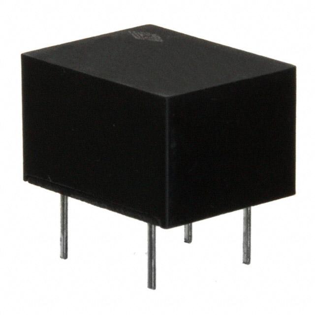
引脚分配: - 引脚1和4:Vin(输入电压) - 引脚2和3:+Vo(输出电压)

参数特性: - 输出功率:0.1W至1W - 电压精度、纹波(20MHz带宽下50mVpp至75mVpp)、噪声(20MHz带宽下75mVpp至150mVpp) - 线路调整率和负载调整率根据不同输出电压有所不同 - 温度系数:0.03%/°C - 开关频率:100%负载下100kHz

功能详解: - 该系列转换器可以提供板载局部电源,具有半调节输出,可以跟随三端调节器以提供输出保护和调节。 - 所有规格在TA-25°C、湿度<75%、正常输入电压和额定输出负载下测量,除非另有说明。

应用信息: - 为确保模块高效可靠运行,最小输出负载不应小于全负载的10%,且产品不应在无负载条件下运行。 - 产品在正常工作条件下的输出电路没有过载保护,可以通过在输入端串联自恢复保险丝或添加电路断路器来实现保护。 - 如果实际输出功率非常小,建议在输出端并联适当电阻以增加负载,或使用额定输出功率较低的产品。

封装信息: - 所有引脚间距为2.54mm(0.1英寸),引脚直径为0.50mm(0.02英寸),公差为±0.25mm(0.01英寸)。
VBSD1-S5-S15-DIP 价格&库存

很抱歉,暂时无法提供与“VBSD1-S5-S15-DIP”相匹配的价格&库存,您可以联系我们找货

免费人工找货