For more information, please visit the product page.
date
09/10/2012
page
1 of 5
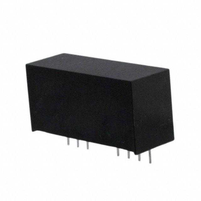
SERIES: VWQBS2-SIP │ DESCRIPTION: DC-DC CONVERTER
2 W isolated output
wide input (4:1)
industry standard 9 pin SIP package
single unregulated outputs
1,500 V isolation
short circuit protection
wide temperature (-40~85°C)
efficiency up to 79%
U
•
•
•
•
•
•
•
•
ED
FEATURES
input
voltage
MODEL
typ
(Vdc)
range
(Vdc)
(Vdc)
24
9.0~36.0
3.3
output
current
output
power
ripple
and noise1
efficiency
min
(mA)
max
(mA)
max
(W)
max
(mVp-p)
typ
(%)
50
500
2
150
68
TI
VWQBS2-Q24-S3.3-SIP
output
voltage
N
RoHS
VWQBS2-Q24-S5-SIP
24
9.0~36.0
5
40
400
2
150
76
VWQBS2-Q24-S9-SIP
24
9.0~36.0
9
22
222
2
150
78
24
9.0~36.0
12
16
167
2
150
79
24
9.0~36.0
15
13
133
2
150
79
N
VWQBS2-Q24-S12-SIP
VWQBS2-Q24-S15-SIP
VWQBS2-Q48-S3.3-SIP
48
18.0~72.0
3.3
50
500
2
150
72
VWQBS2-Q48-S5-SIP
48
18.0~72.0
5
40
400
2
150
75
48
18.0~72.0
9
22
222
2
150
76
48
18.0~72.0
12
16
167
2
150
78
48
18.0~72.0
15
13
133
2
150
79
VWQBS2-Q48-S15-SIP
1. ripple and noise are measured at 20 MHz BW
IS
C
Notes:
O
VWQBS2-Q48-S9-SIP
VWQBS2-Q48-S12-SIP
D
PART NUMBER KEY
Base Number
VWQBS2 - SXX - SXX -SIP
Input Voltage
Output Voltage
cui.com
Packaging Style
�For more information, please visit the product page.
CUI Inc │ SERIES: VWQBS2-SIP │ DESCRIPTION: DC-DC CONVERTER
date 09/10/2012 │ page 2 of 5
INPUT
conditions/description
min
typ
max
units
operating input voltage
24 V model
48 V model
9.0
18.0
24
48
36.0
72.0
Vdc
Vdc
surge voltage
1 second max.
50
100
Vdc
Vdc
1.6
W
24 V model
48 V model
-0.7
-0.7
short circuit input power
input filter
C filter
OUTPUT
input voltage from low to high
load regulation
measured from 10% load to full load
voltage accuracy
see derating curves
positive
negative
transient recovery time
25% load step change
transient response deviation
25% load step change
switching frequency
100% load, input voltage range
PROTECTIONS
TI
temperature coefficient
min
parameter
conditions/description
short circuit protection
continuous, automatic recovery
N
SAFETY AND COMPLIANCE
conditions/description
isolation voltage
for 1 minute at 1 mA max.
isolation resistance
at 500 Vdc
MTBF
RoHS compliant
O
parameter
typ
max
units
±0.2
±0.75
%
±0.5
±1.5
%
±1
±3
±3
±5
%
%
25
ms
±3
±5
%
U
conditions/description
line regulation
N
parameter
ED
parameter
300
kHz
±0.03
%/°C
min
typ
max
units
min
typ
max
units
1,500
Vdc
1,000
MΩ
1,000,000
hours
yes
IS
C
ENVIRONMENTAL
parameter
conditions/description
min
typ
max
units
operating temperature
-40
85
°C
storage temperature
-55
125
°C
storage humidity
non-condensing
temperature rise
at full load
95
lead temperature
1.5 mm from case for 10 seconds
D
15
cui.com
%
°C
300
°C
�For more information, please visit the product page.
CUI Inc │ SERIES: VWQBS2-SIP │ DESCRIPTION: DC-DC CONVERTER
date 09/10/2012 │ page 3 of 5
DERATING CURVES
80
60
40
20
-20
0
20
40
60 71
85
MECHANICAL
100
parameter
conditions/description
dimensions
1.024 x 0.374 x 0.492 (26.00 x 9.50 x 12.50 mm)
case material
plastic (UL94-V0)
MECHANICAL DRAWING
N
units: mm [inches]
tolerance: ±0.25 [±0.010]
pin section tolerance: ±0.10 mm [±0.004]
9.50
[0.374]
O
2.5 0
[0 .098]
26.00[1.024]
(Bo ttom Vie w)
1 2 3
6 78 9
20.32[0.800]
2.54[0.100]
� � �
typ
5.8
� � � �
4.10
[0.161]
12.50
[0.492]
0.50
[0.020]
(Side Vie w)
2.54
[0.100]
cui.com
FUNCTION
1
GND
2
+Vin
3
CTRL
6
+Vo
7
NC
8
NC
9
0V
units
g
∅1.00[0.039]
PIN CONNECTIONS
PIN
max
inch
2.54
[0.100]
20.32[0.800]
IS
C
D
min
TI
weight
120
N
Ambient Temperature (°C)
U
-40
2.50[0.098]
Load (%)
100
ED
1. output power vs. ambient temperature
�For more information, please visit the product page.
CUI Inc │ SERIES: VWQBS2-SIP │ DESCRIPTION: DC-DC CONVERTER
date 09/10/2012 │ page 4 of 5
APPLICATION NOTES
Requirement on Output Load
To ensure this module can operate efficiently and reliably, During operation, the minimum output load is not less than 10% of the full
load, and that this product should never be operated under no load! If the actual output power is very small, please connect a
resistor with proper resistance at the output end in parallel to increase the load, or use our company’s products with a lower rated
output power.
2.
Overload Protection
Under normal operating conditions, the output circuit of these products has no protection against overload. The simplest method is to
connect a self-recovery fuse in series at the input end or add a circuit breaker to the circuit.
24
250
48
150
U
Fuse (slow-blow type)
(mA)
Recommended Circuit
If you want to further decrease the input/output ripple, an “LC” filtering network may be connected to the input and output ends of
the DC/DC converter, see (Figure 1).
Vc
Figure 1
D1 Ic R
Lin
Vin
C1
2
C2
N
3.
Vin
(Vdc)
ED
1.
3
6
+Vo
Cout
1
0V
TI
GND
9
However, the capacitance of the output filter capacitor must be proper. If the capacitance is too big, a startup problem might arise.
For every channel of output, provided the safe and reliable operation is ensured, the greatest capacitance of its filter capacitor see
(Table 1).
Cout
100 μF
N
Input Current(A)
General: Ip ≤1.4*Iin-max
R=
VC-VD-1.0
IC
Ip
Inp ut Voltage
Ra nge
Input Voltage (V)
No parallel connection or plug and play
D
6.
4.7 ~ 120 μH
Input Current
Nominal input voltage range. The input current of the power supply must be sufficient to the startup current (Ip) of the DC-DC
module.
IS
C
5.
10 ~ 100 μF
Lin
CTRL Terminal
When open or high impedance, the converter work well; When this pin is ‘high’; the converter shutdown; It should be note that the
input current should between 5~10 mA,exceeding the maximum 20 mA will cause permanence damage to the converter. The value of
Vc not limited and desirable 5 Vdc, 12 Vdc, or directly with Vin. The value of R can be derived as follows:
O
4.
C1/C2
Table 1
cui.com
�For more information, please visit the product page.
CUI Inc │ SERIES: VWQBS2-SIP │ DESCRIPTION: DC-DC CONVERTER
date 09/10/2012 │ page 5 of 5
REVISION HISTORY
description
date
07/23/2007
1.0
initial release
1.01
new template applied
1.02
V-Infinity branding removed
ED
rev.
04/17/2012
09/10/2012
D
IS
C
O
N
TI
N
U
The revision history provided is for informational purposes only and is believed to be accurate.
Headquarters
20050 SW 112th Ave.
Tualatin, OR 97062
800.275.4899
Fax 503.612.2383
cui.com
techsupport@cui.com
CUI offers a two (2) year limited warranty. Complete warranty information is listed on our website.
CUI reserves the right to make changes to the product at any time without notice. Information provided by CUI is believed to be accurate and reliable. However, no responsibility is
assumed by CUI for its use, nor for any infringements of patents or other rights of third parties which may result from its use.
CUI products are not authorized or warranted for use as critical components in equipment that requires an extremely high level of reliability. A critical
component is any component of a life support device or system whose failure to perform can be reasonably expected to cause the failure of the life support device or system, or to
affect its safety or effectiveness.
�
很抱歉,暂时无法提供与“VWQBS2-Q24-S12-SIP”相匹配的价格&库存,您可以联系我们找货
免费人工找货