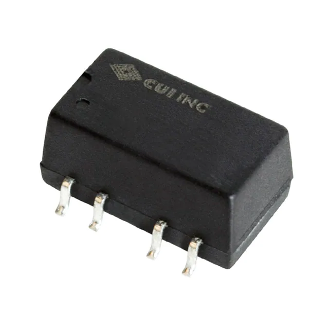
PDS1-S12-D5-M-TR

PDS1-S12-D5-M-TR

  • 厂商:

    CUI

  • 封装:

    SMD6

  • 描述:

    PDS1-S12-D5-M-TR

  • 详情介绍
  • 数据手册
  • 价格&库存
PDS1-S12-D5-M-TR 数据手册
Additional Resources: Product Page | 3D Model | PCB Footprint date 08/09/2022 page 1 of 8 SERIES: PDS1-M │ DESCRIPTION: DC-DC CONVERTER FEATURES • • • • • • • • • • 1 W isolated output smaller package single and dual unregulated outputs 1,500 Vdc isolation short circuit protection extended temperature range (-40~105°C) antistatic protection up to 8kV high efficiency at light load efficiency up to 82% EN 62368-1 MODEL input voltage output voltage output current output power ripple and noise2 efficiency typ (Vdc) range (Vdc) (Vdc) min (mA) max (mA) max (W) typ (mVp-p) typ (%) PDS1-S3-S3-M 3.3 2.97~3.63 3.3 30 303 1 60 69 PDS1-S3-S5-M 3.3 2.97~3.63 5 20 200 1 60 74 PDS1-S3-D5-M 3.3 2.97~3.63 ±5 ±10 ±100 1 60 76 PDS1-S3-D12-M 3.3 2.97~3.63 ±12 ±5 ±42 1 60 77 PDS1-S3-D15-M 3.3 2.97~3.63 ±15 ±3 ±33 1 60 78 1 PDS1-S5-S3-M 5 4.5~5.5 3.3 30 303 1 60 72 PDS1-S5-S5-M1 5 4.5~5.5 5 20 200 1 60 80 PDS1-S5-S9-M 5 4.5~5.5 9 12 111 1 60 80 PDS1-S5-S12-M1 5 4.5~5.5 12 9 84 1 60 80 1 PDS1-S5-S15-M 5 4.5~5.5 15 7 67 1 60 80 PDS1-S5-S24-M1 5 4.5~5.5 24 4 42 1 60 80 PDS1-S5-D5-M 5 4.5~5.5 ±5 ±10 ±100 1 60 80 PDS1-S5-D9-M 5 4.5~5.5 ±9 ±6 ±56 1 60 80 PDS1-S5-D12-M 5 4.5~5.5 ±12 ±5 ±42 1 60 79 PDS1-S5-D15-M 5 4.5~5.5 ±15 ±3 ±33 1 60 81 PDS1-S5-D24-M 5 4.5~5.5 ±24 ±2 ±21 1 60 81 1 PDS1-S12-S3-M 12 10.8~13.2 3.3 30 303 1 60 72 PDS1-S12-S5-M1 12 10.8~13.2 5 20 200 1 60 71 PDS1-S12-S9-M 12 10.8~13.2 9 12 111 1 60 80 PDS1-S12-S12-M1 12 10.8~13.2 12 9 84 1 60 80 PDS1-S12-S15-M 12 10.8~13.2 15 7 67 1 60 80 PDS1-S12-D5-M 12 10.8~13.2 ±5 ±10 ±100 1 60 80 PDS1-S12-D9-M 12 10.8~13.2 ±9 ±6 ±56 1 60 80 PDS1-S12-D12-M 12 10.8~13.2 ±12 ±5 ±42 1 60 73 PDS1-S12-D15-M 12 10.8~13.2 ±15 ±3 ±33 1 60 81 PDS1-S12-D24-M 12 10.8~13.2 ±24 ±2 ±21 1 60 81 PDS1-S15-S15-M 15 13.5~16.5 15 7 67 1 60 80 1 1 1 1 Notes: 1. UL approved 2. Ripple and noise are measured at 20 MHz BW by “parallel cable” method with 1 μF ceramic and 10 μF electrolytic capacitors on the output. cui.com Additional Resources: Product Page | 3D Model | PCB Footprint CUI Inc │ SERIES: PDS1-M │ DESCRIPTION: DC-DC CONVERTER MODEL (CONTINUED) input voltage date 08/09/2022 │ page 2 of 8 output voltage output current output power ripple and noise2 efficiency typ (Vdc) range (Vdc) (Vdc) min (mA) max (mA) max (W) typ (mVp-p) typ (%) PDS1-S24-S5-M1 24 21.6~26.4 5 20 200 1 60 73 PDS1-S24-S9-M1 24 21.6~26.4 9 12 111 1 60 80 PDS1-S24-S12-M 24 21.6~26.4 12 9 84 1 60 80 PDS1-S24-S15-M1 24 21.6~26.4 15 7 67 1 60 72 PDS1-S24-S24-M 24 21.6~26.4 24 4 42 1 60 80 PDS1-S24-D5-M 24 21.6~26.4 ±5 ±10 ±100 1 60 70 PDS1-S24-D9-M 24 21.6~26.4 ±9 ±6 ±56 1 60 80 PDS1-S24-D12-M 24 21.6~26.4 ±12 ±5 ±42 1 60 72 PDS1-S24-D15-M 24 21.6~26.4 ±15 ±3 ±33 1 60 71 PDS1-S24-D24-M 24 21.6~26.4 ±24 ±2 ±21 1 60 80 1 Notes: 1. UL approved 2. Ripple and noise are measured at 20 MHz BW by “parallel cable” method with 1 μF ceramic and 10 μF electrolytic capacitors on the output. PART NUMBER KEY PDS1 - SXX - XXX - M - X Base Number Input Voltage Output S = single D = dual Output Voltage Packaging Style SMT Package Options "blank" = standard TR = Tape & Reel INPUT parameter conditions/description min typ max units operating input voltage 3.3 Vdc input models 5 Vdc input models 12 Vdc input models 15 Vdc input models 24 Vdc input models 2.97 4.5 10.8 13.5 21.6 3.3 5 12 15 24 3.63 5.5 13.2 16.5 26.4 Vdc Vdc Vdc Vdc Vdc surge voltage for maximum of 1 second 3.3 Vdc input models 5 Vdc input models 12 Vdc input models 15 Vdc input models 24 Vdc input models -0.7 -0.7 -0.7 -0.7 -0.7 5 9 18 21 30 Vdc Vdc Vdc Vdc Vdc filter capacitance filter max units ±1.5 ±1.2 % % OUTPUT parameter conditions/description min line regulation for Vin change of 1% 3.3 Vdc output models all other models load regulation measured from 10% load to full load 3.3 Vdc output models 5 Vdc output models 9 Vdc output models 12 Vdc output models 15 Vdc output models 24 Vdc output models voltage accuracy see tolerance envelope curve switching frequency 100% load, nominal input voltage temperature coefficient 100% load typ 18 12 8 7 6 5 % % % % % % 100 kHz ±0.03 cui.com %/°C Additional Resources: Product Page | 3D Model | PCB Footprint CUI Inc │ SERIES: PDS1-M │ DESCRIPTION: DC-DC CONVERTER date 08/09/2022 │ page 3 of 8 PROTECTIONS parameter conditions/description short circuit protection1 3 & 24 Vdc input models PDS1-S5-S12-M, PDS1-S5-D24-M all other models: automatic recovery Note: min typ max units 1 1 s s max units 1. The supply voltage must be discontinued at the end of the short circuit duration SAFETY AND COMPLIANCE parameter conditions/description isolation voltage input to output for 1 minute at 1 mA max. 1,500 Vdc isolation resistance input to output at 500 Vdc 1,000 MΩ isolation capacitance input to output at 100 kHz/0.1 V safety approvals2 certified to 62368-1: EN certified to 60950-1: UL conducted emissions CISPR32/EN55032, class B (external circuit required, see Figure 1) radiated emissions CISPR32/EN55032, class B (external circuit required, see Figure 1) ESD IEC/EN 61000-4-2, class B, contact ±8kV (single output models) IEC/EN 61000-4-2, class B, contact ±6kV (dual output models) MTBF as per MIL-HDBK-217F @ 25 °C RoHS Note: min typ 20 pF 3,500,000 hours 2011/65/EU 2. See specific models noted on pages 1 & 2 ENVIRONMENTAL parameter conditions/description min operating temperature see derating curve storage temperature storage humidity non-condensing temperature rise at full load, Ta=25°C typ max units -40 105 °C -55 125 °C 95 % 25 °C SOLDERABILITY parameter conditions/description max units hand soldering 1.5 mm from case for 10 seconds min 300 °C reflow soldering see reflow soldering profile 245 °C 25 0 24 5 Peak .Temp 245˚C( Max.) 21 7 Tem peratur e (˚C ) 20 0 60 Sec Max ( >217˚ C) 15 0 10 0 50 0 typ Tim e (se c.) cui.com Additional Resources: Product Page | 3D Model | PCB Footprint CUI Inc │ SERIES: PDS1-M │ DESCRIPTION: DC-DC CONVERTER date 08/09/2022 │ page 4 of 8 MECHANICAL parameter conditions/description dimensions single output models: 12.7 x 8.30 x 7.25 dual output models: 15.24 x 8.30 x 7.25 min case material epoxy resin (UL94-V0) weight single output models dual output models SINGLE OUTPUT MODELS units: mm[inch] tolerance: ±0.25[±0.010] pin section tolerance: ±0.10[±0.004] PIN CONNECTIONS Function 1 GND 2 Vin 4 0V 5 +Vo 8 NC cui.com max units mm mm 1.6 2.0 MECHANICAL DRAWING PIN typ g g Additional Resources: Product Page | CUI Inc │ SERIES: PDS1-M │ DESCRIPTION: DC-DC CONVERTER DUAL OUTPUT MODELS units: mm[inch] tolerance: ±0.25[±0.010] pin section tolerance: ±0.10[±0.004] PIN CONNECTIONS Function 1 GND 2 Vin 4 0V 5 -Vo 7 +Vo 10 NC | PCB Footprint date 08/09/2022 │ page 5 of 8 MECHANICAL DRAWING (CONTINUED) PIN 3D Model cui.com Additional Resources: Product Page | 3D Model | PCB Footprint CUI Inc │ SERIES: PDS1-M │ DESCRIPTION: DC-DC CONVERTER date 08/09/2022 │ page 6 of 8 DERATING CURVES EMC RECOMMENDED CIRCUIT Figure 1 Table 1 Recommended external circuit components Single Outputs Dual Outputs Vout (dc) Cin LDM Cout CY 3.3 4.7μF/50V 6.8μH 10μF - 5 4.7μF/50V 6.8μH 10μF - 9 4.7μF/50V 6.8μH 4.7μF - 12 4.7μF/50V 6.8μH 2.2μF - 15 4.7μF/50V 6.8μH 1μF - 24 4.7μF/50V 6.8μH 0.47μF - ±5 4.7μF/50V 6.8μH 4.7μF - ±9 4.7μF/50V 6.8μH 2.2μF - ±12 4.7μF/50V 6.8μH 1μF - ±15 4.7μF/50V 6.8μH 1μF 1nF/2kV ±24 4.7μF/50V 6.8μH 0.47μF 1nF/2kV Note: cui.com 1. See Cout values in Tables 1 and 2. 2. 24 Vdc output models require CY also. Additional Resources: Product Page | 3D Model | PCB Footprint CUI Inc │ SERIES: PDS1-M │ DESCRIPTION: DC-DC CONVERTER date 08/09/2022 │ page 7 of 8 APPLICATION NOTES 1. Output load requirement To ensure this module can operate efficiently and reliably, the minimum output load may not be less than 10% of the full load during operation. If the actual output power is low, connect a resistor at the output end in parallel to increase the load. 2. Overload Protection Under normal operating conditions, the output circuit of this product has no protection against overload. The simplest method to add this is to add a circuit breaker to the circuit. 3. Recommended circuit If you want to further decrease the input/output ripple, you can increase the capacitance accordingly or choose capacitors with low ESR (see Figure 2 & Table 1). However, the capacitance of the output filter capacitor must be appropriate. If the capacitance is too high, a startup problem might arise. For every channel of the output, to ensure safe and reliable operation, the maximum capacitance must be less than the maximum capacitive load (see Table 2). It’s not recommended to connect any external capacitors in applications with less than 0.5 watt output. Figure 2 Single Outputs Dual Outputs Table 2 Single Vout (Vdc) Max. Capacitive Load (μF) Dual Vout (Vdc) Max. Capacitive Load1 (μF) 3.3 220 - - 5 220 ±5 100 9 220 ±9 100 12 220 ±12 100 15 220 ±15 100 24 220 ±24 100 Note: 4. 1. For each output. Output Voltage Regulation and Over-voltage Protection Circuit The device for output voltage regulation, over-voltage and over-current protection is a linear regulator and a capacitor filtering ne work with overheat protection which can be connected to the input or output end in series (see Figure 3). The recommended capacitance of its filter capacitor (see Table 1 & 2), and the linear regulator is based on the actual voltage and current required. Figure 3 Single Outputs Note: 1. 2. 3. 4. Dual Outputs Operation under minimum load will not damage the converter; however, they may not meet all specifications listed. Max. capacitive load tested at input voltage range and full load. It is recommended to use either ceramic capacitors or electrolytic capacitors on the input and the output. Using tantalum capacitors may increase the risk of failure. All specifications measured at: Ta=25°C, humidity
PDS1-S12-D5-M-TR
物料型号:PDS1-M系列,包括多个型号,如PDS1-S12-S5-M1等。

器件简介:PDS1-M系列是DC-DC转换器,具备1W隔离输出、小尺寸封装、单双路非稳压输出、1500V直流隔离、短路保护、扩展温度范围(-40~105°C)、防静电保护高达8kV、轻载高效率(最高82%)等特点,并符合EN 62368-1标准。

引脚分配:单路输出模型有5个引脚,双路输出模型有7个引脚,具体包括GND、Vin、OV、+Vo、-Vo、NC等。

参数特性:输入电压范围从3.3Vdc到24Vdc,输出电压从3.3Vdc到±24Vdc,输出电流从3.3mA到30mA,最大输出功率为1W,纹波和噪声典型值为60mVp-p。

功能详解:PDS1-M系列转换器提供了多种输出配置和保护特性,如短路保护和自动恢复、隔离电压高达1500Vdc等。

应用信息:产品适用于需要高效率和高可靠性DC-DC转换的应用场合,但不建议用于生命支持设备或系统。

封装信息:单路输出模型尺寸为12.7x8.30x7.25mm,双路输出模型尺寸为15.24x8.30x7.25mm,采用环氧树脂封装材料。

PDS1-S12-D5-M-TR 价格&库存

很抱歉,暂时无法提供与“PDS1-S12-D5-M-TR”相匹配的价格&库存,您可以联系我们找货

免费人工找货