Additional Resources:
Product Page
|
3D Model
|
PCB Footprint
date
06/29/2021
page
1 of 5
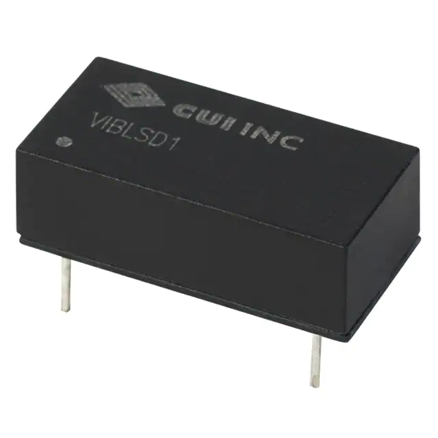
SERIES: VIBLSD1-DIP │ DESCRIPTION: DC-DC CONVERTER
FEATURES
•
•
•
•
•
•
•
1 W isolated output
industry standard 14 pin DIP package
single regulated outputs
1,000 V isolation
short circuit protection
wide temperature (-40~85°C)
efficiency up to 75%
RoHS
MODEL
input
voltage
output
voltage
output
current
output
power
ripple1
noise1
efficiency
typ
(Vdc)
range
(Vdc)
(Vdc)
min
(mA)
max
(mA)
max
(W)
max
(mVp-p)
max
(mVp-p)
typ
(%)
VIBLSD0.75-S5-S5-DIP
5
4.75~5.25
5
15
150
0.75
20
75
68
VIBLSD1-S5-S5-DIP
5
4.75~5.25
5
20
200
1
20
75
67
VIBLSD1-S5-S9-DIP*
5
4.75~5.25
9
12
111
1
20
75
70
VIBLSD1-S5-S12-DIP
5
4.75~5.25
12
9
83
1
20
75
71
VIBLSD1-S5-S15-DIP*
5
4.75~5.25
15
7
67
1
20
75
73
VIBLSD1-S5-S24-DIP*
5
4.75~5.25
24
5
42
1
20
75
68
VIBLSD0.75-S12-S5-DIP
12
11.4~12.6
5
15
150
0.75
20
75
68
VIBLSD1-S12-S5-DIP
12
11.4~12.6
5
20
200
1
20
75
67
VIBLSD1-S12-S9-DIP
12
11.4~12.6
9
12
111
1
20
75
72
VIBLSD1-S12-S12-DIP
12
11.4~12.6
12
9
83
1
20
75
70
VIBLSD1-S12-S15-DIP
12
11.4~12.6
15
7
67
1
20
75
74
VIBLSD1-S12-S24-DIP*
12
11.4~12.6
24
5
42
1
20
75
68
VIBLSD0.75-S24-S5-DIP
24
22.8~25.2
5
20
200
0.75
20
75
68
VIBLSD1-S24-S5-DIP
24
22.8~25.2
5
15
150
1
20
75
68
VIBLSD1-S24-S9-DIP*
24
22.8~25.2
9
12
111
1
20
75
68
VIBLSD1-S24-S12-DIP*
24
22.8~25.2
12
9
83
1
20
75
73
VIBLSD1-S24-S15-DIP*
24
22.8~25.2
15
7
67
1
20
75
75
VIBLSD1-S24-S24-DIP
24
22.8~25.2
24
5
42
1
20
75
68
Notes:
1. ripple and noise are measured at 20 MHz BW
*. Discontinued model
PART NUMBER KEY
VIBLSDX - SXX - SXX -DIP
Base Number
Output Power
Output Voltage
Input Voltage
cui.com
Packaging Style
�Additional Resources:
Product Page
|
3D Model
|
PCB Footprint
CUI Inc │ SERIES: VIBLSD1-DIP │ DESCRIPTION: DC-DC CONVERTER
date 06/29/2021 │ page 2 of 5
INPUT
parameter
conditions/description
min
typ
max
units
operating input voltage
5 V model
12 V model
24 V model
4.75
11.4
22.8
5
12
24
5.25
12.6
25.2
Vdc
Vdc
Vdc
parameter
conditions/description
min
typ
max
units
line regulation
for Vin change of ±5%
±0.25
%
load regulation
measured from 10% load to full load
±1
%
voltage accuracy
100% load
switching frequency
100% load, input voltage range
OUTPUT
±3
temperature coefficient
%
100
kHz
±0.03
%/°C
PROTECTIONS
parameter
conditions/description
short circuit protection
5 and 24 V output models
all other models: continuous
min
typ
max
units
1
s
max
units
SAFETY AND COMPLIANCE
parameter
conditions/description
isolation voltage
for 1 minute at 1 mA max.
isolation resistance
at 500 Vdc
min
MTBF
RoHS compliant
typ
1,000
Vdc
1,000
MΩ
3,500,000
hours
yes
ENVIRONMENTAL
parameter
conditions/description
min
typ
max
units
operating temperature
-40
85
°C
storage temperature
-55
125
°C
storage humidity
non-condensing
temperature rise
at full load
lead temperature
1.5 mm from case for 10 seconds
15
cui.com
95
%
25
°C
300
°C
�Additional Resources:
Product Page
|
3D Model
|
PCB Footprint
CUI Inc │ SERIES: VIBLSD1-DIP │ DESCRIPTION: DC-DC CONVERTER
date 06/29/2021 │ page 3 of 5
DERATING CURVES
MECHANICAL
parameter
conditions/description
dimensions
20.00 x 10.00 x 7.00 (0.787 x 0.394 x 0.276 inch)
min
case material
plastic (UL94-V0)
typ
max
units
mm
weight
2.4
g
MECHANICAL DRAWING
����
>�����@
�����>�����@
�����>�����@
�����
>�����@
����>�����@
��
��
����> �����@
�
Front View
PCB Layout
Top View
�����>�����@
�����>�����@
�
��
����>�����@
�����>�����@
PIN CONNECTIONS
�
��
�
����
>�����@
�����
>�����@
�����>�����@
�����>�����@
�
����
>�����@
�����
>�����@
Bottom View
cui.com
PIN
FUNCTION
1
GND
7
NC
9
+Vo
11
0V
14
Vin
����
>�����@
�����
>�����@
units: mm [inches]
tolerance: ±0.25 [±0.010]
pin section tolerance: ±0.10 [±0.004]
�Additional Resources:
Product Page
|
3D Model
|
PCB Footprint
CUI Inc │ SERIES: VIBLSD1-DIP │ DESCRIPTION: DC-DC CONVERTER
date 06/29/2021 │ page 4 of 5
APPLICATION NOTES
1. Requirement on Output Load
In order to ensure the product operates efficiently and reliably, make sure the specified range of input voltage is not exceeded and the
minimum output load is not less than 10% load. If the actual load is less than the specified minimum load, the output ripple may
increase sharply while its efficiency and reliability will reduce greatly. If the actual output power is very small, please add an
appropriate resistor as extra loading.
2. Overload Protection
Under normal operating conditions, the output circuit of these products has no protection against over-current and short-circuits. The
simplest method is to connect a self-recovery fuse in series at the input end or add a circuit breaker to the circuit.
3. Filtering
In some circuits which are sensitive to noise and ripple, a filtering capacitor may be added to the DC/DC output end and input end to
reduce the noise and ripple. However, the capacitance of the output filter capacitor must be proper. If the capacitance is too big, a
startup problem might arise. For every channel of output, provided the safe and reliable operation is ensured, the greatest
capacitance of its filter capacitor sees the external capacitor table. To get an extremely low ripple, an “LC” filtering network may be
connected to the input and output ends of the DC/DC converter, which may produce a more significant filtering effect. It should also
be noted that the inductance and the frequency of the “LC” filtering network should be staggered with the DC/DC frequency to avoid
mutual interference (Figure 1).
Figure 1
4. Output Voltage Regulation and Over-voltage Protection Circuit
The simplest device for output voltage regulation, over-voltage and over-current protection is a linear voltage regulator with overheat
protection that is connected to the input or output end in series (Figure 2).
Figure 2
5. External Capacitor Table
It is not recommended to connect any external capacitor in the application field with less than 0.5 W output.
Table 1
Note:
Vin
(Vdc)
Cin
(µF)
Vout
(Vdc)
Cout
(µF)
5
4.7
5
10
12
4.7
9
4.7
15
2.2
12
2.2
24
1
15
1
--
--
24
0.47
All specifications measured at 25°C, humidity
VIBLSD1-S12-S24-DIP 价格&库存
很抱歉,暂时无法提供与“VIBLSD1-S12-S24-DIP”相匹配的价格&库存,您可以联系我们找货
免费人工找货