Additional Resources:
Product Page
date
08/22/2013
page
1 of 5
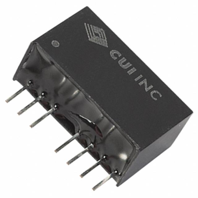
SERIES: VWRAS2-SIP │ DESCRIPTION: DC-DC CONVERTER
2 W isolated output
wide input (2:1)
industry standard 8 pin SIP package
dual regulated outputs
1,500 V isolation
short circuit protection
wide temperature (-40~85°C)
efficiency up to 79%
U
•
•
•
•
•
•
•
•
ED
FEATURES
input
voltage
MODEL
typ
(Vdc)
range
(Vdc)
(Vdc)
5
4.5~9
output
current
output
power
ripple
and noise1
efficiency
min
(mA)
max
(mA)
max
(W)
max
(mVp-p)
typ
(%)
±5
±20
±200
2
100
67
TI
VWRAS2-D5-D5-SIP
output
voltage
N
RoHS
5
4.5~9
±9
±11
±111
2
100
71
5
4.5~9
±12
±8
±83
2
100
72
VWRAS2-D5-D15-SIP
5
4.5~9
±15
±7
±67
2
100
73
VWRAS2-D12-D5-SIP
12
9~18
±5
±20
±200
2
100
73
N
VWRAS2-D5-D9-SIP
VWRAS2-D5-D12-SIP
VWRAS2-D12-D9-SIP
12
9~18
±9
±11
±111
2
100
74
VWRAS2-D12-D12-SIP
12
9~18
±12
±8
±83
2
100
78
12
9~18
±15
±7
±67
2
100
77
24
18~36
±5
±20
±200
2
100
76
VWRAS2-D24-D9-SIP
VWRAS2-D24-D12-SIP
VWRAS2-D24-D15-SIP
24
18~36
±9
±11
±111
2
100
78
24
18~36
±12
±8
±83
2
100
79
24
18~36
±15
±7
±67
2
100
78
48
36~72
±5
±20
±200
2
100
75
IS
C
VWRAS2-D48-D5-SIP
O
VWRAS2-D12-D15-SIP
VWRAS2-D24-D5-SIP
VWRAS2-D48-D9-SIP
48
36~72
±9
±11
±111
2
100
78
VWRAS2-D48-D12-SIP
48
36~72
±12
±8
±83
2
100
79
VWRAS2-D48-D15-SIP
48
36~72
±15
±7
±67
2
100
79
Notes:
1. ripple and noise are measured at 20 MHz BW
D
PART NUMBER KEY
Base Number
VWRAS2 - DXX - DXX -SIP
Input Voltage
Output Voltage
cui.com
Packaging Style
�Additional Resources:
Product Page
CUI Inc │ SERIES: VWRAS2-SIP │ DESCRIPTION: DC-DC CONVERTER
date 08/22/2013 │ page 2 of 5
INPUT
conditions/description
min
typ
max
units
operating input voltage
5 V model
12 V model
24 V model
48 V model
4.5
9.0
18.0
36.0
5
12
24
48
9.0
18.0
36.0
72.0
Vdc
Vdc
Vdc
Vdc
parameter
conditions/description
min
line regulation
input voltage from low to high
load regulation
measured from 10% load to full load
voltage accuracy
input voltage range refer to output load
switching frequency
100% load, input voltage range
continuous
SAFETY AND COMPLIANCE
parameter
conditions/description
isolation voltage
for 1 minute at 1 mA max.
isolation resistance
at 500 Vdc
RoHS compliant
yes
ENVIRONMENTAL
min
conditions/description
±0.5
±1.0
%
±1
±3
%
500
max
units
typ
max
units
Vdc
1,000
MΩ
1,000,000
hours
min
typ
max
units
-40
85
°C
-50
125
°C
15
1.5 mm from case for 10 seconds
D
cui.com
kHz
%/°C
typ
non-condensing
at full load
IS
C
lead temperature
%
1,500
O
storage humidity
temperature rise
min
N
MTBF
N
conditions/description
short circuit protection
TI
parameter
storage temperature
units
±0.03
PROTECTIONS
operating temperature
max
±0.5
180
temperature coefficient
parameter
typ
±0.2
U
OUTPUT
ED
parameter
95
%
35
°C
300
°C
�Additional Resources:
Product Page
CUI Inc │ SERIES: VWRAS2-SIP │ DESCRIPTION: DC-DC CONVERTER
date 08/22/2013 │ page 3 of 5
DERATING CURVES
ED
1. output power vs. ambient temperature
80
60
40
20
-20
0
20
40
60 71
85
Ambient Temperature (°C)
parameter
conditions/description
dimensions
0.866 x 0.374 x 0.472 (22.00 x 9.50 x 12.00 mm)
case material
plastic (UL94-V0)
min
TI
weight
12 3
5678
9.50
(0.374)
(Bottom View)
O
1 .3 0
(0 .0 51 )
N
units: mm [inches]
tolerance: ±0.25 [±0.010]
pin section tolerance: ±0.10 mm [±0.004]
2
3
5
6
IS
C
2. 54[ 0. 100]
PIN CONNECTIONS
D
(Side View)
4.10
(0.161)
22.00 (0.866)
cui.com
5.5
7 8
2.54
(0.100)
2.10
(0.083)
PIN
FUNCTION
1
GND
2
+Vin
3
CTRL
5
NC
6
+Vo
7
0V
8
-Vo
max
units
inch
∅1.00 [0.039]
2.10 [0.083]
1
typ
2 . 5 4[ 0. 1 0 0]
MECHANICAL DRAWING
12.00
(0.472)
0.50
(0.020)
120
N
MECHANICAL
100
U
-40
2. 50 [0 .0 98 ]
Load (%)
100
g
�Additional Resources:
Product Page
CUI Inc │ SERIES: VWRAS2-SIP │ DESCRIPTION: DC-DC CONVERTER
date 08/22/2013 │ page 4 of 5
APPLICATION NOTES
CTRL Terminal
When open or high impedance,the converter work well; When this pin is ‘high’; the converter shutdown; It should be noted that the
input current (Ic) should between 5-10mA, exceeding the maximum 20mA will cause permanent damage to the converter. The value
of R can be derived as follows :
VC-VD-1.0
R=
IC
ED
1.
Recommended Circuit
If you want to further decrease the input/output ripple, an “LC” filtering network may be connected to the input and output ends of
the DC/DC converter, see (Figure 1).
Figure 1
Vin
(Vdc)
D1 Ic R
L in 2
V in
3
6
L ou t
+Vo
Cou t
C in
0V
7
Cou t
L ou t
1
GN D
-Vo
Lin
(μH)
Cout
(μF)
Lout
(μH)
5
100
4.7~120
100
2.2~10
12
100
4.7~120
100
2.2~10
24
10~22
4.7~120
100
2.2~10
48
10~22
4.7~120
100
2.2~10
N
8
Cin
(μF)
U
Vc
TI
However, the capacitance of the output filter capacitor must be proper. If the capacitance is too big, a startup problem might arise. To
ensure safe and reliable operation see Table 1 for the maximum capacitance of each channel of output.
±5
560
±9
470
±12
330
±15
270
Input Curent
While using unstable power source, please ensure the output voltage and ripple voltage do not excced indexes of the converter. The
preceding power source must be able to provide for converter sufficient starting current Ip.
O
2.
Cout
(μF)
N
Table 1
Vout
(Vdc)
No parallel connection or plug and play
Ip
Inp ut Voltage
Ra nge
Input Voltage (V)
D
3.
Input Current(A)
IS
C
General: Ip ≤1.4*Iin-max
Note:
1. All specifications measured at Ta = 25°C, humidity
很抱歉,暂时无法提供与“VWRAS2-D24-D9-SIP”相匹配的价格&库存,您可以联系我们找货
免费人工找货